FOR LOW VOLTAGE OPERATIONS
FEATURES
■ FROM 3V TO 5.5V V
■ MINIM U M O U TPUT VO L T A GE AS LO W AS
0.6V.
■ 1V TO 28V INPUT VOLTAGE RANGE.
■ CONSTANT ON TIME TOPOLOGY ALLO WS .
OPERATION WITH VERYLOW AND HIGH
DUTY CYCLES.
■ VERY FAST LOAD TRANSIENTS.
■ 0.6V, ±1% VREF.
■ SELECTABLE SINKING MODE.
■ LOSSLESS CURRENT LIMIT, AVAILABLE
ALSO IN SINKING MODE
■ REMOTE SENSING.
■ OVP,UVP LATCHED PROTECTIONS.
■ 600µA TYP QUIESCENT CURRENT.
■ POWER GOOD AND OVP SIGNALS.
■ PULSE SKIPPING AT LIGTH LOADS.
■ 94% EFFICIENCY FROM 3.3V TO 2.5V.
APPLICATIONS
■
NETWORKING.
■
DC/DC MODULES.
■
DISTRIBUTED POWER.
■
MOBILE A PPLICATIONS.
■
CHIP SET, CPU, DSP AND MEMORIES SUPPLY.
RANGE.
CC
L6997
STEP DOWN CONTROLLER
TSSOP20
ORDERING NUMBERS: L6997D
L6997DTR
DESCRIPTION
The device is a high efficient solution for networking
dc/dc modules and mobile application compatible
with 3.3V bus and 5V bus.
It's able to regulate an output vol tage as low as 0.6V.
The constant on time topology assures fast load tran-
sient response. The embedded voltage feed-forward
provides nearly constant switching frequency operation.
An integrator can be introduced in the control loop to
reduce the static output voltage error.
The remote sensing improv es the static and dynamic
regulation, recovering the wires voltage drop.
Pulse skipping technique reduces power consumption at light loads. Drivers current capability allows
output currents in excess of 20A.
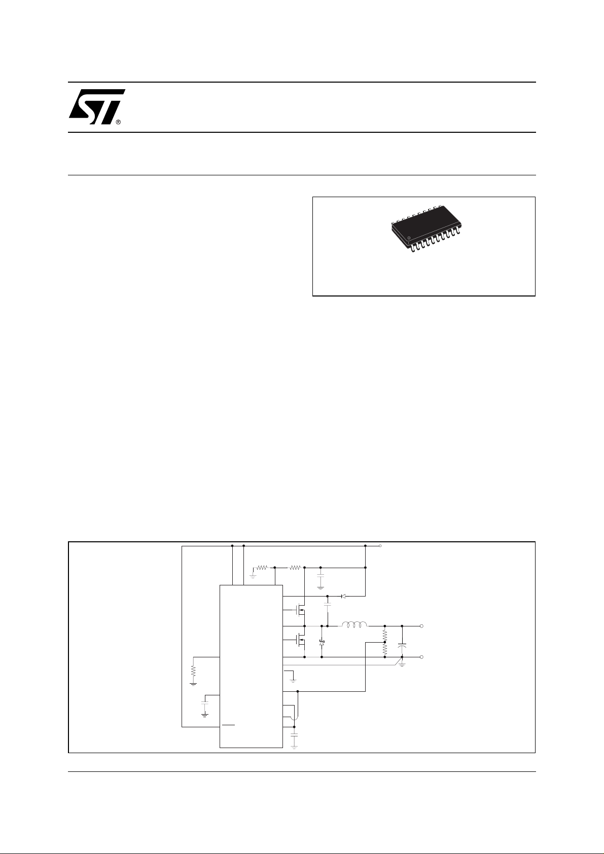
MINIMUM COMPONENT COUNT APPLICATION
VDR
L6997
OSC
BOOT
HGATE
PHASE
LGATE
PGND
GND
GNDSENSE
VSENSE
INT
VFB
Vref
VCC
PGOOD
OVP
ILIM
Rilim
SS
Css
SHDN
April 2003
3.3V
Rin1Rin2
Cin
Dboot
HS
Cboot
Cvref
L
DS
LS
Ro1
Ro2
0.6V
Cout
1/23
L6997
ABSOLUTE MAXIMUM RATINGS
Symbol Parameter Value Unit
V
CC
V
DR
V
PHASE
P
tot
T
stg
THERMAL DATA
Symbol Parameter Value Unit
VCC to GND -0.3 to 6 V
V
to GND -0.3 to 6 V
DR
HGATE and BOOT, to PHASE -0.3 to 6 V
HGATE and BOOT, to PGND -0.3 to 36 V
PHASE -0.3-to 30 V
LGATE to PGND -0.3 to V
ILIM, VFB, VSENSE, NOSKIP, SHDN, PGOOD, OVP, VREF, INT,
SENSE
to GND
= 25°C 1 W
amb
GND
Power dissipation at T
-0.3 to V
+0.3 V
DR
+0.3 V
CC
Storage temperature range -40 to 150 °C
R
th j-amb
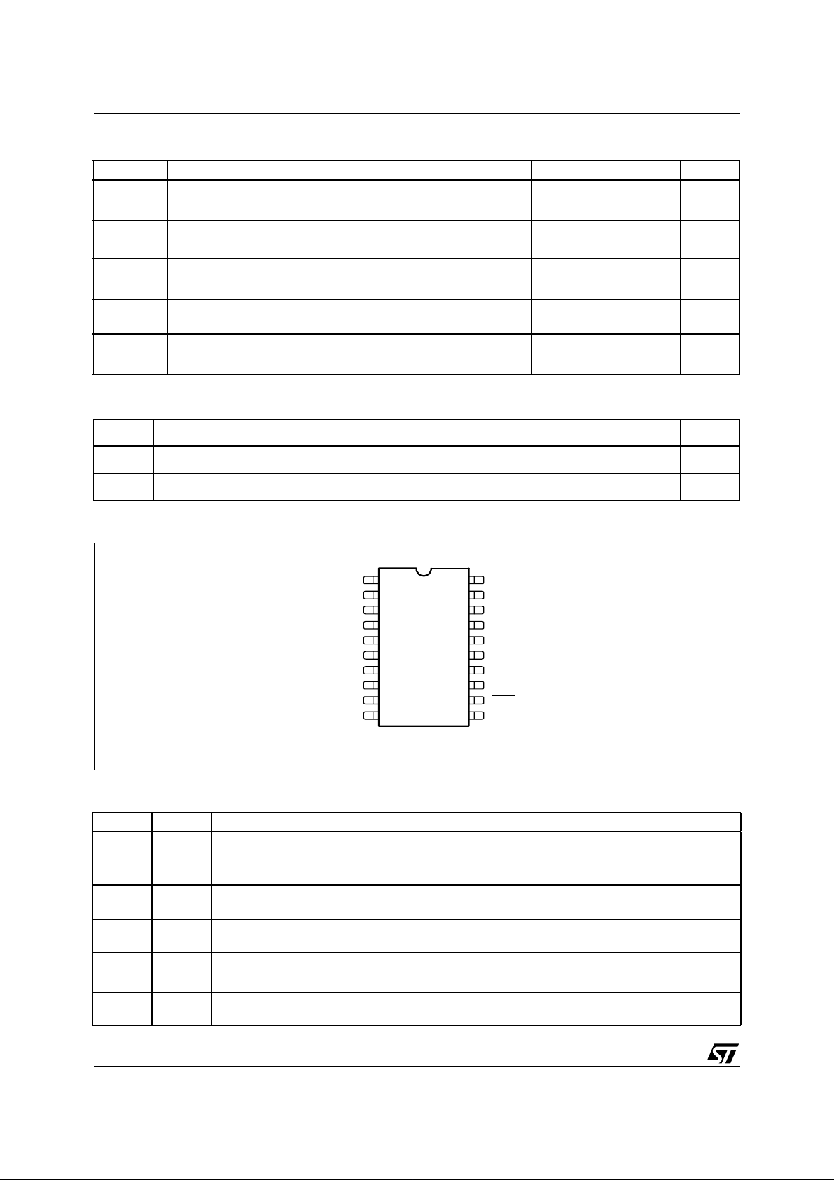
PIN CONNECTION
Thermal Resistance Junction to Ambient 125 °C/W
T
Junction operating temperature range -40 to 125 °C
j
(Top View)
NOSKIP
GNDSENSE
INT
INT
VSENSE
VCC
GND
VREF
VFB
OSC
2
3
4
5
6
7
8
9
10SS
TSSOP20
20
BOOT1
19
HGATE
18
PHASE
17
VDR
16
LGATE
15
PGND
14
PGOOD
13
OVP
12
SHDN
11
ILIM
PIN FUNCTION
N° Name Description
1 NOSKIP Connect to V
2 GNDSE
Remote ground sensing pin
NSE
3 INT Integrator output. Short this pin to VFB pin and connect it via a capacitor to V
integrator in the control loop. If the integrator is not used, short this pin to VREF.
4 VSENSEThis pin must be connected to the remote output voltage to detect overvoltage and undervoltage
conditions and to provide integrator feedback input.
5V
IC Supply Voltage.
CC
6 GND Signal ground
7 VREF 0.6V voltage reference. Connect max. a 10nF ceramic capacitor between this pin and ground.
This pin is capable to source or sink up to 250uA
to force continuous conduction mode and sink mode.
CC
to insert the
OUT
2/23

L6997
PIN FUNCTION
(continued)
N° Name Description
8 VFB PWM comparator feedback input. Short this pin to INT pin when using the integrator function, or
to VSENSE pin without integrator.
9 OSC Connect this pin to the input voltage through a voltage divider in order to provide the feed-
forward function. It cannot be left floating.
10 SS Soft start pin. A 5µA constant current charges an external capacitor which value sets the soft-
start time.
11 ILIM An external resistor connected between this pin and GND sets the current limit threshold.
12 SHDN Shutdown. When connected to GND the device and the drivers are OFF. It cannot be left floating.
13 OVP Open drain output. During the over voltage condition it is pulled up by an external resistor.
14 PGOOD Open drain output. During the soft start and in case of output voltage fault it is low. It is pulled up
by external resistor.
15 PGND Low Side driver ground.
16 LGATE Low Side driver output.
17 V
Low Side driver supply.
DR
18 PHASE Return path of the High Side driver.
19 HGATE High side MOSFETS driver output.
20 BOOT Bootstrap capacitor pin. High Side driver is supplied through this pin.
ELECTRICAL CHARACTERISTICS
= VDR = 3.3V; T
(V
CC
= 0°C to 85°C unless otherwise specified)
amb
Symbol Parameter Test Condition Min. Typ. Max. Unit
SUPPLY SECTION
Vin Input voltage range Vout=Vref Fsw=110Khz Iout=1A 1 28 V
V
,
CC
V
DR
V
Turn-onvoltage 2.86 2.97 V
CC
3 5.5 V
Tu r n-off voltage 2.75 2 .9 V
Hysteresis 90 mV
IqV
Quiescent Current Drivers VFB > VREF 7 20 µA
DR
IqVcc Device Quiescent current VFB > VREF 400 600 µA
SHUTDOWN SECTION
SHDN Device On 1.2 V
Device Off 0.6 V
I
SHVDR
I
SHVCC
Drivers shutdown current SHDN to GND 5 µA
Devices shutdown current SHDN to GND 1 15 µA
SOFT START SECTION
I
Soft Start current VSS = 0.4V 4 6 µA
SS
Active Soft start and voltage 300 400 500 mV
CURRENT LIMIT AND ZERO CURRENT COMPARATOR
ILIM input bias current R
Zero Crossing Comparator offset
= 2KΩ to 200KΩ 4.6 5 5.4 µA
ILIM
-2 2 mV
Phase-gnd
DK
Current limit factor 1.6 1.8 2 µA
ILIM
3/23

L6997
ELECTRICAL CHARACTERISTICS
(V
= VDR = 3.3V; T
CC
= 0°C to 85°C unless otherwise specified)
amb
(continued)
Symbol Parameter Test Condition Min. Typ. Max. Unit
ON TIME
Ton On time duration V
REF=VSENSE OSC
V
REF=VSENSE OSC
V
REF=VSENSE OSC
=125mV 720 800 880 ns
=250mV 370 420 470 ns
=500mV 210 240 270 ns
OFF TIME
T
OFFMIN
Minimum off time 600 ns
K
OSC/TOFFMIN
OSC=250mV 0.3 0.33
VOLTAGE REFERENCE
VREF Voltage Accuracy 0µA < I
< 100µA 0.594 0.6 0.606 V
REF
PWM COMPARATOR
Input voltage offset -2 +2 mV
I
Input Bias Current 20 nA
FB
INTEGRATOR
INT Over Voltage Clamp V
INT Under Voltage Clamp V
Integrator Input Offset Voltage
V
SENSE-VREF
I
VSENSE
Input Bias Current 20 nA
= V
SENSE
SENSE
CC
= GND 0.45 0.55 0.65 V
0.62 0.75 0.88 V
-4 -4 mV
GATE DRIVERS
High side rise time V
High side fall time 50 100 ns
Low side rise time V
Low side fall time 50 90 ns
P
UVP/OVP PROTECTIONS
GOOD
=3.3V; C=7nF
DR
HGATE - PHASE from 1 to 3V
=3.3V; C=14nF
DR
LGATE from 1 to 3V
OVP Over voltage threshold with respect to V
REF
118 121 124 %
50 90 ns
50 90 ns
UVP Under voltage threshold 67 70 73 %
PGOOD Upper threshold
(V
SENSE-VREF
)
PGOOD Lower threshold
)
V
PGOOD
(V
SENSE-VREF
V
rising 110 112 116 %
SENSE
V
falling 85 88 91 %
SENSE
I
=2mA 0.2 0.4 V
Sink
4/23
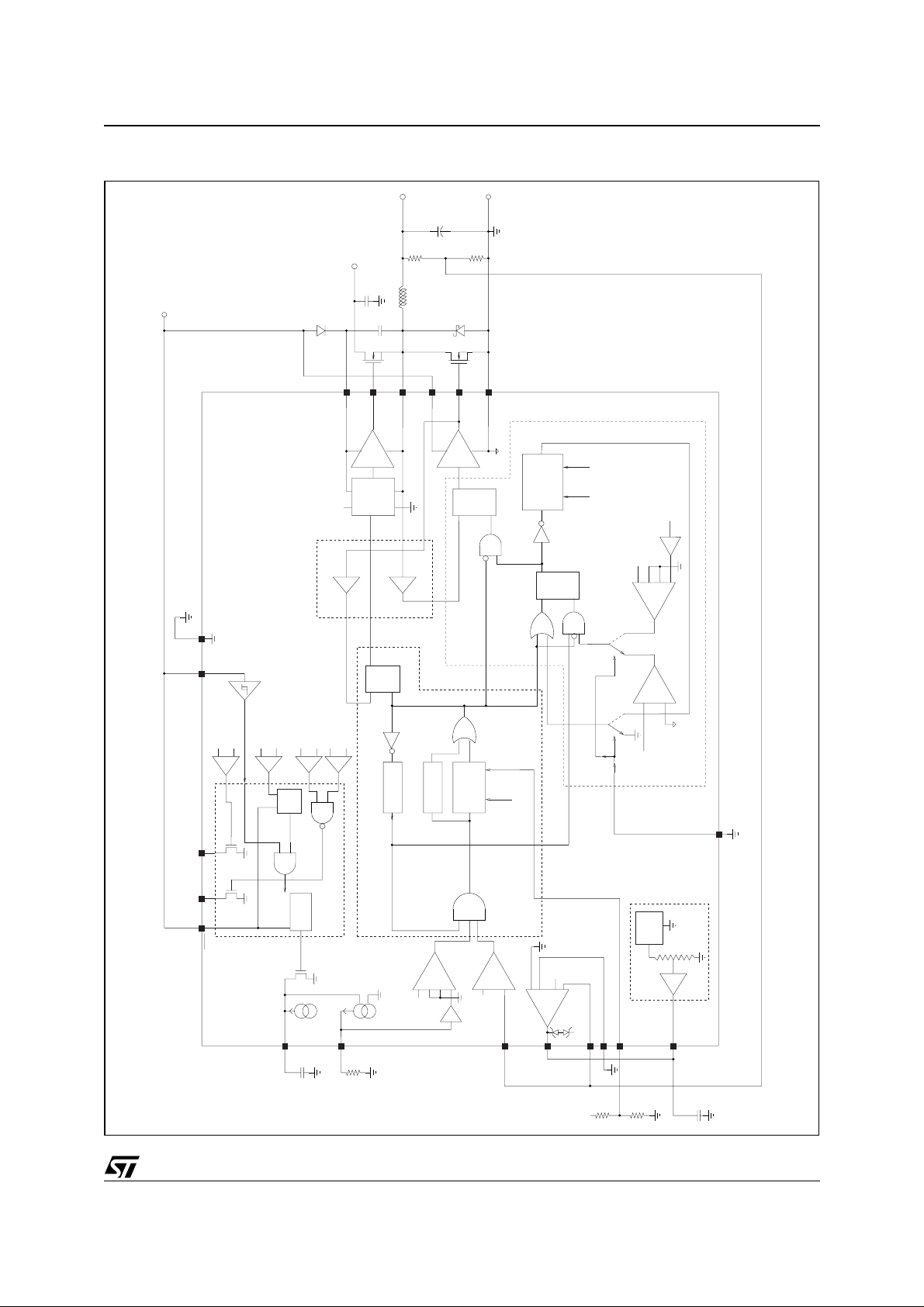
Figure 1. Funct i on a l & Blo c k D iag ram
IN
V
Vcc
L6997
OUT
V
GNDVCCOVPPGOODSHDN
overvoltage comparator
VSENSE
+
1.12 VREF
-+undervoltage comparator
VSENSE
0.6 VREF
pgood comparators
SR
LS and HS anti-cross-conduction comparators
VSENSE
1.075 VREF
-
+
comp
V(LGATE)<0.5V
VSENSE
+
BOOT
VCC
0.925 VREF
-
HGATE
HS driver
level shifter
V(PHASE)<0.2V
Q
R
comp
S
Toff min
PHASE
delay
VDR
Ton min
one-shot
PGND
LGATE
LS driver
Q
R
S
Ton
one-shot
Ton
OSC
VSENSE
Q
S
one-shot
OSC
VSENSE
Ton= Kosc V(VSENSE)/V(OSC)
R
no-skipno-skip
mode
mode
comparator
negative current limit
PHASE
++-
-
+
PHASE
ILIM
0.05
zero-cross comparator
LS control
Ton= Kosc V(VSENSE)/V(OSC)
NOSKIP
IC enable
control
soft-start
SS
5 uA
power management
ILIM
positive current limit
comparator
-
PHASE
+-+
+VREF
0.05
FB
HS control
VREF
pwm comparator
-
-
-
+
+
Gm
VREF
INT
VSENSE
IN
V
SENSEGND
OSC
1.236V
bandgap
VREF
1.416
Reference chain
0.6V
5/23
L6997
1 DEVICE DESCRIPTION
1.1 Constant On Time PWM topology
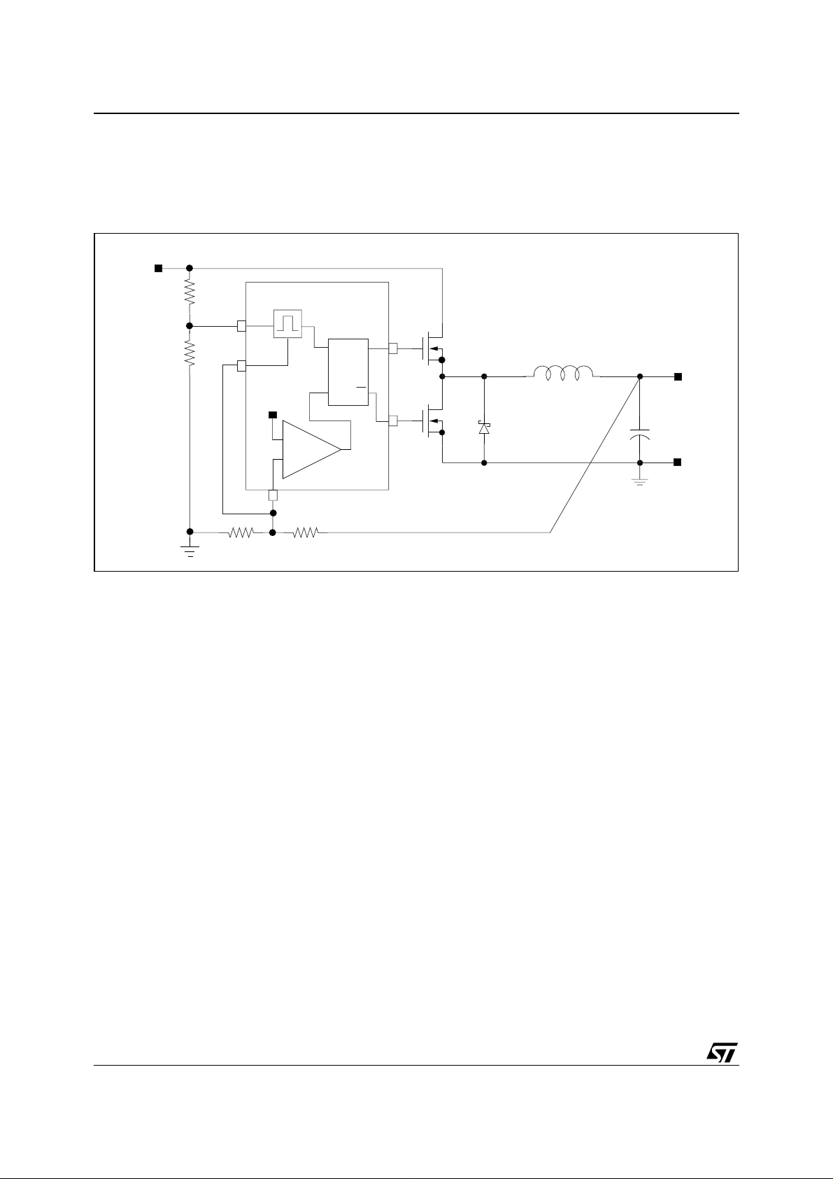
Figure 2. Loop block schematic diagram
Vin
R1
R2
One-shot generator
OSC
Vsense
Vref
FFSR
Q
R
HGATE
S
Q
+
LGATE
HS
LS
Vout
DS
-
PWM comparator
FB
R4
R3
The device implements a Constant On Time control scheme, where the Ton is the high side MOSFET on time
duration forced by the one-shot generator. The on time is directly proportional to VSENSE pin voltage and inverse to OSC pin voltage as in Eq1:
V
SENSE
Eq 1
where K
T
ON
= 250ns and τ is the internal propagation delay time (typ. 70ns). The system imposes in steady
OSC
state a minimum on time corresponding to V
responding Ton will not decrease. Connecting the OSC pin to a voltage partition from V
steady-state switching frequency F
V
Eq 2
f
-------------- -
== =
SW
K
OSC
OUT
V
IN
--------------------- -
V
OSC
1
---------- -
T
ON
τ+=
= 1V. In fact if the V
OSC
independent of VIN. It results:
SW
α
-------------- -
α
OSC
OUT
1
-------------- -
K
OSC
α
→ fSWK
OSC
OSC
OSCαOUT
voltage increases above 1V the cor-
to G N D, it a l lows a
IN
where
V
Eq 3
Eq 4
α
OSC
α
OUT
OSC
-------------- -
V
IN
V
FB
-------------- -
V
OUT
The above equations allow setting the frequency div ider ratio
such equations hold only if V
independent from the input voltage. The delay introduces a light dependenc e from V
R
2
--------------------==
R2R1+
R
4
--------------------==
R3R4+
α
once output voltage has been s et; note that
<1V. Further the Eq2 shows how the system h as a sw itching frequenc y ideall y
OSC
OSC
. A minimum off-time con-
IN
strain of about 500ns is introduced in order to assure the boot capacitor charge and to limit the switching fre-
6/23
L6997
quency after a load transient as well as to mask PWM comparator output against noise and spikes.
The system has not an internal clock, b ecause this is a hysteretic control ler, so the turn on puls e will start if three
conditions are met contemporarily : the FB pin voltage i s low er than the refere nce voltage, the minimum o ff time
is passed and the current limit comparator is not triggered (i.e. the inductor current is below the current limit
value). The voltage on the OSC pin must range between 50mV and 1V to ensure the system linearity.
1.2 Closing the loop
The loop is closed connecting the output voltage (or the output divider middle point) to the FB pin. The FB pin
is linked internally to the comparator negative pin and the positive pin is connected to the reference voltage
(0.6V Typ.) as in Figure 2. When the FB goes lower than the reference voltage, the PWM comparator output
goes high and sets the flip-flop outpu t, turning on the hig h side MOSFET. This condition i s latched to av oid noise
spike. After the on-time (calculated as descr ibed in the previous section) the system resets the flip-flop and then
turns off the high side MOSFET and turns on the low side MOSFET. Internally the device has more complex
logic than a flip-flop to manage the transition in correct way. For more details refers to the Figure 1.
The voltage drop along ground and supply metals connecting output capacitor to the load is a source of DC
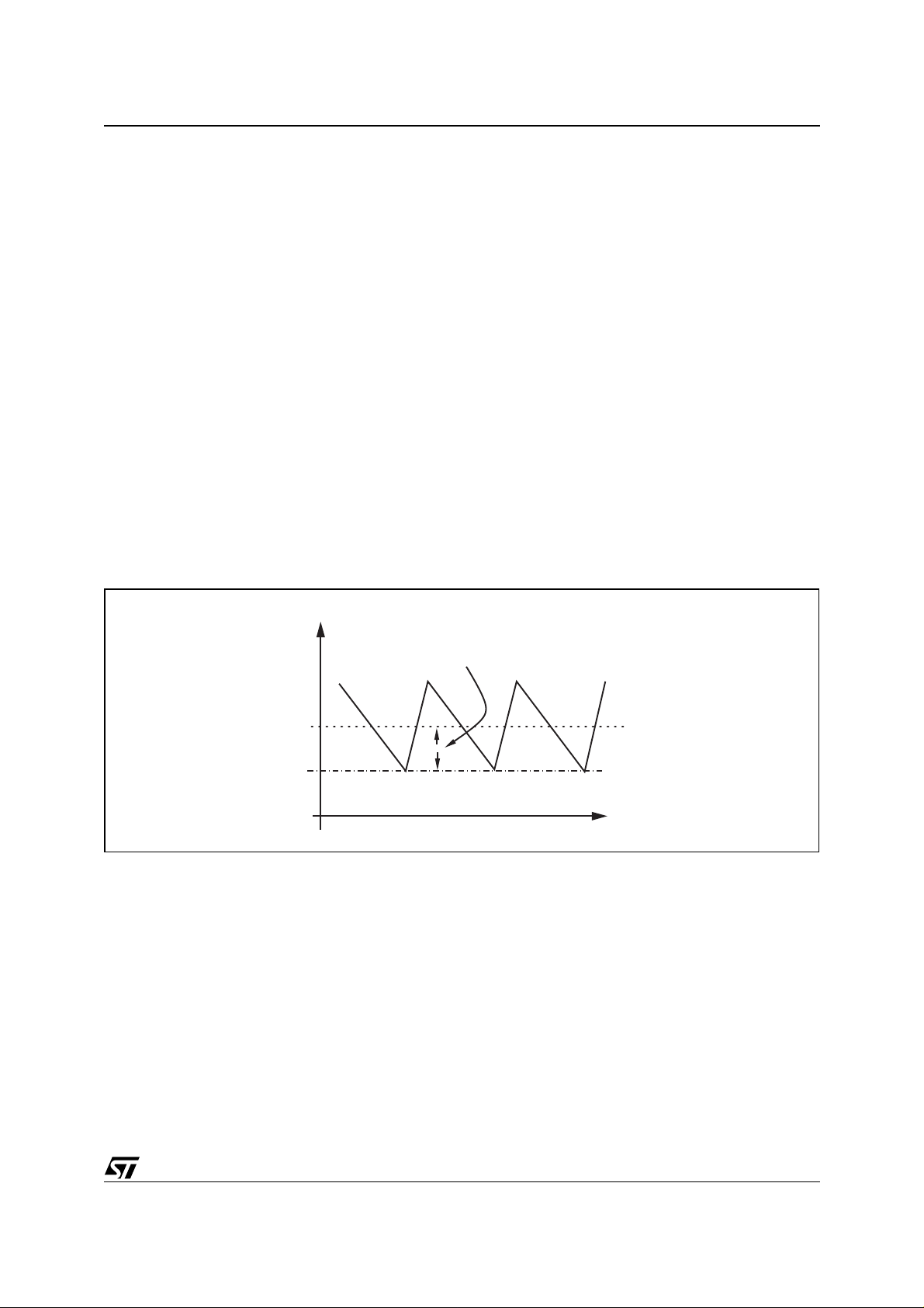
error. Further the system r egulates the o utput voltage v alley v alue not the aver age, as in the Fi gure 3 is show n.
So the voltage ripple on the output capacitor is a source of DC static error (as the PCB traces). To compensate
the DC errors, an integrator network must be introduced in the control lo op, by connectin g the output voltage to
the INT pin through a capacitor and the FB pin to the INT pin directly as in Figure 4. The internal integrator amplifier with the exter nal capac itor C
for output ripple.
introduces a D C pole i n the contr ol l oop. C
INT1
also provides an AC path
INT1
Figure 3. Valle y regulation
Vout
DC Error Offset
<Vout>
Vref
Time
The integrator amplifier generates a current, proportional to the DC errors, that increases the output capacitance
voltage in order to c ompensate the total static er rors. A v oltage clamper within the device forces IN T pi n v oltage
ranges from V
-50mV, V
REF
+150mV. This is useful to avoid or smooth output voltage overshoot during a load
REF
transient. Also, this means that the integrator is capable of recovering output error due to ripple when its peakto-peak amplitude is less than 150mV in steady state.
In case of the ripple amplitude is larger than 150mV, a capacitor C
can be connected between INT pin and
INT2
ground to reduce r ipple amplitu de at INT pin, otherw ise the integrator can operate out of its linear range. Choose
C
according to the following equation:
INT1
g
⋅
Eq 5
C
INT1
where GINT=50 µs is the integrator transconductance,
is the close loop bandwidth. This equation also holds if C
INTαOUT
------------------------------ -=
⋅⋅
2 π F
u
α
is the output divider ratio given from Eq4 and F
OUT
is connected between INT pin and ground. C
INT2
INT2
is given by:
U
7/23
 Loading...