

SGS Thomson Microelectronics L6996DTR, L6996D Datasheet
DINAMICALLY PROGRAMMABLE SYNCHRONOUS
V
STE P DOWN CONTROLLER FOR MOBILE CP Us
■
5 BIT DAC WITH AVAILABLE EXTERNAL
OUTPUT VOL TAGE.
■
0.6 TO 1.750V, DYNAMICALLY ADJUSTABLE
OUTPUT VOLTAGE RANGE.
■
±1% OUTPUT ACCURACY OVER LINE AND LOAD.
■
ACTIVE DROOP.
■
CONSTANT ON TIME TOPOLOG Y ALLO WS
LOW DUTY CYCLE AND FAST LOAD
TRANSIENT.
■
90% EFFICIENCY FROM 12V TO 1.35V/8A.
■
1.750V TO 28V BATTERY INPUT RANGE.
■
OPERATING FREQUENCY UP TO 1MHZ.
■
INTEGRATED HIGH CURRENT DRIVERS.
■
LATCHED OVP AND UVP PROTECTIONS.
OCP PROTECTION.
■
350µA TYP. QUIESCENT CURRENT.
■
7µA TYP. SHUTDOWN SUPPLY CURRE N T.
■
PGOOD AND OVP SIGNALS.
■
ZERO-CURRENT DETECTION AND PULSEFREQUENCY MODE.
APPLICATIONS
■
ADVANCED MOBILE CPUs SUPPLY WITH
DYNAMIC TRANSITIONS.
■
NOTEBOOK/LAPTOP, CONCEPT PC CPUs
SUPPLY.
■
DC/DC FROM BATTERY SUPPLY EQUIPMENTS.
L6996
TSSOP24
ORDERING NUMB ERS : L6996D (TSSOP24)
L6996DTR (Tape & Reel)
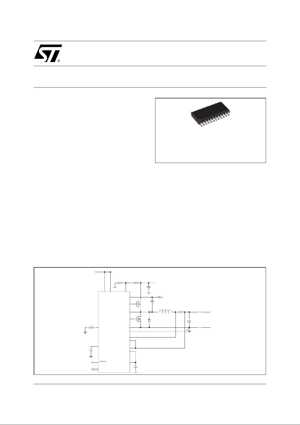
DESCRIPTION
The device is dc -dc controll er specifically designed to
provide extremely high efficiency conversion for mobile advanced microprocessors.
The "constant on-time" topology assures fast load
transient response. The embedded "voltage feedforward" provides nearly constant switching frequency
operation.
A precise 5-bit DAC allows select output v oltage from
0.6V to 1V with 25mV steps and from 1V to 1.75V
with 50mV steps.
L6996 is capable of supporting CPUs VID combination changing during normal operation.
The active droop allows adjust both the output loadline slope and the zero-load output voltage.
APPLICATION DIAGRAM
C
SS
July 2002
5V
25V
PGOOD
OVP
ILIM
SS
SHDN
VID4:0
VDR
VCC
L6996
OSC
BOOT
HGATE
PHASE
LGATE
PGND
GND
CS+
VFB-
VFB+
VPROG
HS
LS
CS-
C
VPROG
5V
L
R
V
SENSE
OUT
1.25
DS
1/26
L6996
ABSOLUTE MAXIMUM RATINGS
Symbol
Parameter
Value Unit
V
CC
V
DR
VCC to GND -0.3 to 6 V
V
to GND -0.3 to 6 V
DR
HGATE and BOOT, to PHASE -0.3 to 6 V
HGATE and BOOT, to PGND -0.3 to 36 V
V
PHASE
PHASE -0.3 to 30 V
LGATE to PGND -0.3 to VDR+0.3 V
ILIM, VFB+, VFB-, CS-, CS+, SHDN, VID0-4, PGOOD, OVP,
-0.3 to VCC+0.3 V
VPROG to GND
P
tot
T
T
stg
Maximum Power dissipation at T
Junction operating temperature range 0 to 125 °C
j
= 25°C 1 W
amb
Storage temperature range -55 to 125 °C
THERMA L D ATA
Symbol Parameter Value Unit
R
th j-amb
Thermal Resistance Junction to Ambient 125 °C/ W
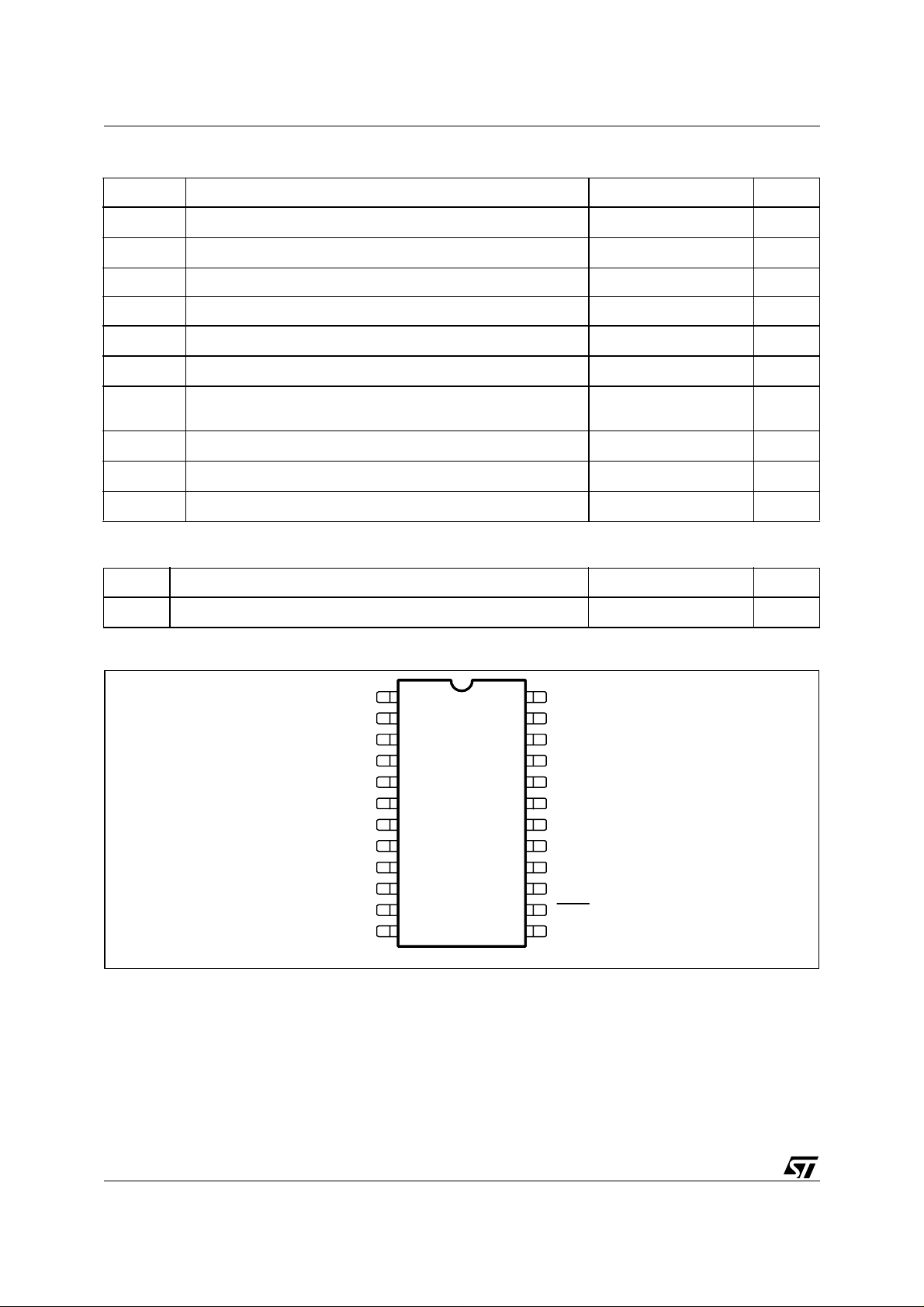
PIN CONNECTION
VID2
VID1
VID0
CS-
CS+
VCC
GND
VPROG
VFB+
VFBOSC
SS
2
3
4
5
6
7
8
9
10
11
12
TSSOP24
24
23
22
21
20
19
18
17
16
15
14
13
VID31
VID4
BOOT
HGATE
PHASE
VDR
LGATE
PGND
PGOOD
OVP
SHDN
ILIM
2/26

PIN FUNCTIONS
N Name Description
L6996
1,2,3,
23,24
4 CS- This pin is used for both current sensing and to detect overvoltage and undervoltage
5 CS+ Current sense pin. Overcurrent condition is detected by sensing CS+ to CS- voltage.
6 VCC Supply voltage for analogy blocks. Connect it to 5V bus.
7 GND Signal ground
8 VPROG DAC output voltage. This pin provides the voltage programmed by the DAC. Connect a 10nF
9 VFB+ PWM comparator reference input. Connect this pin to VPROG.
10 VFB- PWM comparator feedback input, to be connected to the regulated output.
11 OSC Connect this pin to the battery through a voltage divider in order to provide the voltage
12 SS Soft start pin. 5µA constant current charges an external capacitor whose value sets the soft-
13 ILIM An external resistor connected between this pin and GND sets the current limit threshold.
VID4-0 V oltage Identification inputs. VID0 is the LSB and VID4 is the MSB for the DAC (see VID table)
conditions.
capacitor between this pin and GND.
An additional external voltage divider between output and VPROG may be used to realize the
active droop function.
By inserting a resistor between this pin and the regulated output, a positive offset can be
added to the output voltage.
feedforward feature.
start time.
14 SHDN
15 OVP Open drain output. The pull-down transistor is off either in OV condition or during a VID
16 PGOOD Open drain output. The pull-down transistor is on during soft-start, dynamic transitions and
17 PGND Po wer Ground. This pin has to be connected close to the low side MOSFET source in order to
18 LGATE Lower MOSFET gate driver output.
19 V
20 PHASE This pin provides the return path of the high side driver.
21 HGATE High side MOSFET driver output.
22 BOOT Bootstrap capacitor pin. The high side driver is supplied through this pin.
DR
ShutDown input. When connected to GND the device stops working. When high, it enables
the IC operation.
transition.
when an output voltage fault occurs.
minimize switching noise.
Voltage supply for the low side internal driver.
3/26

L6996
ELECTRICAL CHARACTERISTICS
(VCC = VDR = 5V; T
Symbol Parameter Test Condition Min. Typ. Max. Unit
SUPPLY SECTION
Vin Input voltage range Vout=1V Fsw=110Khz Iout=1A 1 28 V
Vcc, V
DR
Vccoff Turn-off voltage 4.1 4.3 V
V
HYST
Iqcc
(V
Iqcc
(Vcc)
SHUTDOWN SECTION
SHDN SHDN Threshold 0.6 1.2 V
I
(VDR)
I
SH
SOFT START SECTION
I
ON TIME
Ton On time duration Vprog=CS- =1.15 Osc=250mV 720 800 880 ns
OFF TIME
DAC
Vprog Voltage Accuracy VID0-4 see table 1 -1 +1 %
PWM COMPARATOR
I
VFB-
CURRENT LIMIT AND ZERO CURRENT COMPARATOR
I
PHASE-
GND
GATE DRIVERS
PROTECTIONS
OVP Over voltage trip CS- rising 117 120 123 %
UVLO Hysteresys 60 90 100 mV
Quiescent current driver VFB- > VFB+ 20 µA
)
DR
Quiescent current VFB- > VFB+ 600 µA
Driver quiescent current in
SH
shutdown.
(Vcc) Shut down current SHDN to GND 15 µA
SS charge current 4 6 µA
SS
Soft-start active range 0.9 V
Minimum Off Time 580 ns
K
OSC/TOFFMIN
Input voltage offset V
Input bias current (VP) V
ILIM input bias current CS-=V
LIM
K
Positive and negative Current
C
Limit factor.
Zero Crossing Comparator offset -2 2 mV
High side rise time V
High side fall time 50 70 ns
Low side rise time 50 70 ns
Low side fall time 50 70 ns
= 0°C to 70°C unless otherwise specified)
amb
SHDN to GND 5 µA
Vprog=CS-= 1.15 Osc= 500m V 355 420 485 ns
Vprog=CS-= 1.15 Osc= 1V 210 250 290 ns
Vprog=CS-= 1.15 Osc= 2V 120 150 180 ns
OSC=250mV
PROG
VFB-
V
=1.6V=V
=1.6V 4 5 6 µA
=1.6V
PROG
ILIM to GND = 120KΩ
R
= 120 KΩ 0.18 0.3 0.24 µA
ILIM
=5V; C=7nF
DR
HGATE - PHASE from 2 to 4.5V
PROG
FB-
=CS-=1.15V
4.5 5.5 V
0.28
-2 +2 mV
4.95 µA
50 70 ns
4/26
L6996
ELECTRICAL CHARACTERISTICS
(V
= VDR = 5V; T
CC
Symbol Parameter Test Condition Min. Typ. Max. Unit
UVP Under voltage trip CS- falling 66 69 72 %
PGOOD Upper threshold
PGOOD Lower threshold
Ron
P
GOOD
(CS-/V
(CS-/V
= 0°C to 70°C unless otherwise specified)
amb
)
PROG
)
PROG
(continued)
CS- rising; PGOOD active 109 112 115 %
CS- falling; PGOOD active 84 87 90 %
I
=2mA 40 60 100 Ω
SOURCE
Table 1. DAC Output Voltage
VID4 VID3 VID2 VID1 VID0 Output Voltage (V)
11 1 1 1 0.600
11 1 1 0 0.625
11 1 0 1 0.650
11 1 0 0 0.675
11 0 1 1 0.700
11 0 1 0 0.725
11 0 0 1 0.750
11 0 0 0 0.775
10 1 1 1 0.800
10 1 1 0 0.825
10 1 0 1 0.850
10 1 0 0 0.875
10 0 1 1 0.900
10 0 1 0 0.925
10 0 0 1 0.950
10 0 0 0 0.975
01 1 1 1 1.000
01 1 1 0 1.050
01 1 0 1 1.100
01 1 0 0 1.150
01 0 1 1 1.200
01 0 1 0 1.250
01 0 0 1 1.300
01 0 0 0 1.350
00 1 1 1 1.400
00 1 1 0 1.450
00 1 0 1 1.500
00 1 0 0 1.550
00 0 1 1 1.600
00 0 1 0 1.650
00 0 0 1 1.700
00 0 0 0 1.750
5/26

L6996
Figure 1. Funct i on a l & Blo c k D iag ram
IN
V
5V
OUT
V
GNDVCC
overvoltage comparator
BOOT
HGATE
HS driver
VCC
level shifter
V(LGATE)<0.5V
comp
LS and HS anti-cross-conduction comparators
R Q
0.6 VPROG
CS-
1.12 VPROG
CS+
-
+
-
undervoltage comparator
RS
pgood comparators
CS-
CS-
1.075 VPROG
0.925 VPROGpower management
+
-
+
-
PHASE
comp
V(PHASE)<0.2V
S
Toff min
delay
VDR
Ton min
one-shot
PGND
LGATE
LS driver
Q
R
S
Ton
one-shot
Ton
OSC
CS-
Q
S
one-shot
OSC
CS-
R
negative current limit
comparator
Ton= Kosc V(CS-)/V(OSC)
CS+
-
mode
dynamic
transition
+
mode
dynamic
transition
PHASE
80 us
one-shot
ILIM
0.05
CS-
-
+
+
zero-cross comparator
Ton= Kosc V(CS-)/V(OSC)
detection
transition
dynamic
6/26
OVPPGOODSHDN
VID4:0
dynamic transition control
IC enable
soft-start
control
+
+
-
comparator
positive current limit
5 uA
SS
ILIM
CS+
CS-
+
-
0.05
FB+
HS control
pwm comparator
5 uA
FB-
OSC
IN
V
1.236V
bandgap
5 bit DAC
1.416
VPROG
VID4:0
DAC
LS control
Reference chain
configuration

TYPICAL OPERATING CHARACTE RISTICS
The test conditions refer to the component list the table 5. VIN = 20V V
unless otherwise noted.
Figure 2. Dynamic Output Voltage Transition
Figure 5. Sta rt up with Zero Load
1.55V -> 1.35V
= 1.8V FSW = 270kHz T
OUT
amb
L6996
= 25°C
CH1 -> V
CH2 -> V
CH4 -> IL
PHASE
OUT
Figure 3. Dynamic Output Voltage Transition
1.35V -> 1.55V
CH1 -> V
CH2 -> V
CH4 -> IL
PHASE
OUT
Figure 6. Start up w ith 10A
CH1 -> V
CH2 -> SS
CH3 -> I
CH1 -> V
CH2 -> SS
CH3 -> I
L
OUT
L
OUT
Figure 4. Load Transient 0-15A
CH1 -> V
CH2 -> V
CH4 -> IL
OUT
OUT
7/26
L6996
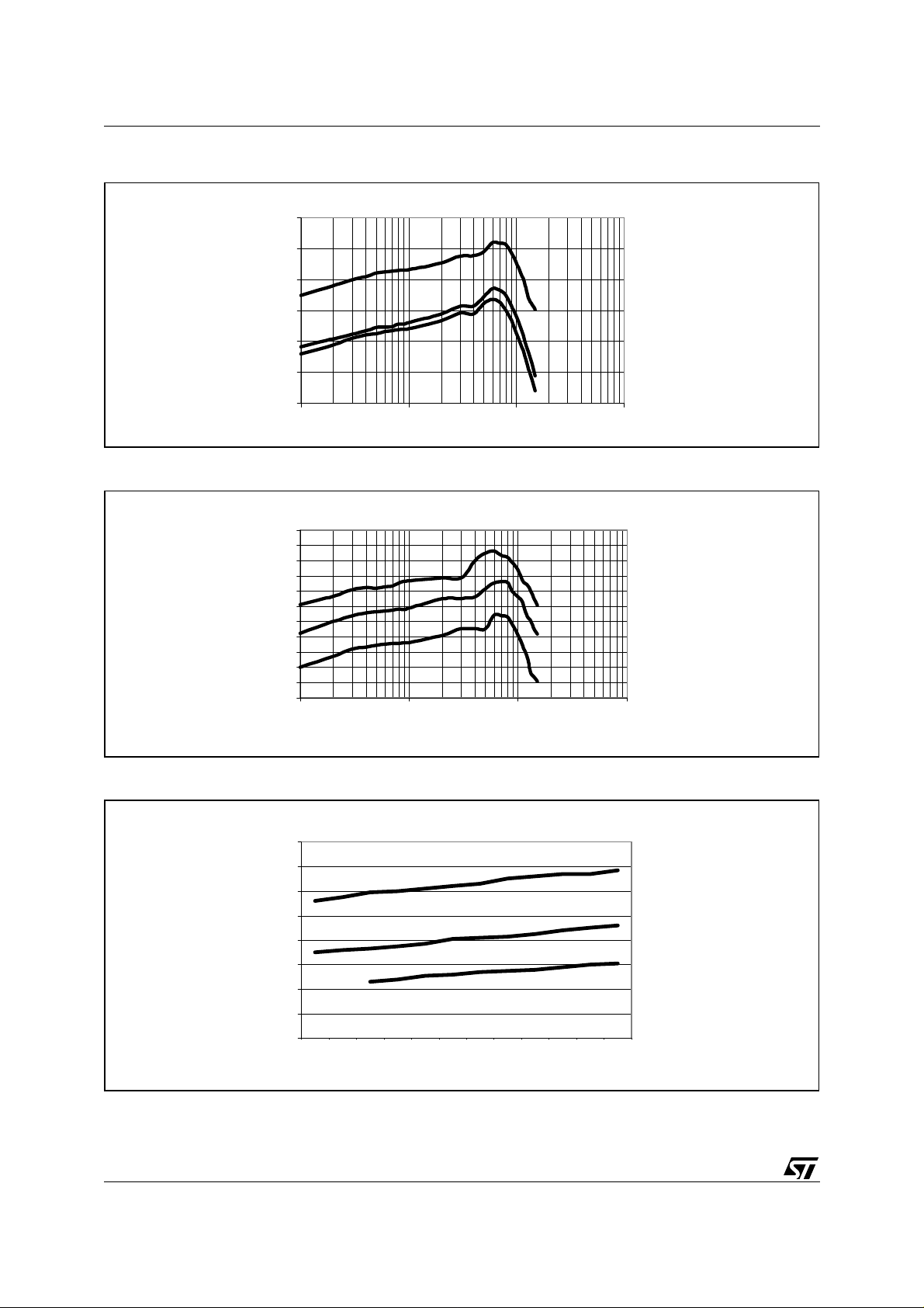
Figure 7. Tes t Condition: Vin = 20V, V5v=5V, Fsw = 300kHz, T
[%]
Vout=1.7
Vout=1.25
Current [A ]
[%]
Vin=7
Vin=20
Current [A]
0.88
0.86
0.84
0.82
0.8
0.78
0.76
Figure 8. Tes t Condition: V
0.92
0.91
0.9
0.89
0.88
0.87
0.86
0.85
0.84
0.83
0.82
0.81
Efficency
Vout=1.35
0.10 1.00 10.00 100.00
= 1.75V, Fsw = 300kHz, V5v = 5V, T
out
Efficency
0.1 1.0 10.0 10 0.0
amb
Vin=12
= +25°C
= +25°C
amb
Figure 9. Tes t Condition: V
410
390
370
350
330
310
290
270
250
8/26
= 1.75V, V5v = 5V, T
out
Frequency
Vin=7
Vin=12
4 5 6 7 8 9 10 11 12 13 14 15
= +25°C
amb
[KHz]
Vin=20
Current [A]
 Loading...