STEP DOWN CONTROLLER FOR HIGH DIFFERENTIAL
FEATURE
■ CONSTANT ON TIME TOPOLOG Y ALLO WS
OPERATION WITH LOWER DUTY THAN
PWM TOPOLOGY
■ VERY FAST LOAD TRANSIENTS
■ 5V V
■ 1.5V TO 28V INPUT VOLTAGE RANGE
■ 0.9V ±1% V
■
■ SELECTABLE SINKING MODE
■ LOSSLESS CURRENT LIMIT
■ REMOTE SENSING
■ OVP,UVP LATCHED PROTECTIONS
■ 600µA TYP QUIESCENT CURRENT
■ POWER GOOD AND OVP SIGNALS
■ PULSE SKIPPING AT LIGHT LOADS
APPLICATIONS
■ I/O BUS FOR CPU CORE SUPPLY
■ NOTEBOOK COMPUTERS
■ NETWORKING DC-DC
■ DISTRIBUTED POWER
SUPPLY
cc
REF
MINIMUM OUTPUT VOLTAGE AS LOW AS 0.9V
L6995
INPUT-OUTPUT CONVERSION
TSSOP20
ORDERING NUMBERS: L6995D
L6995DTR
DESCRIPTION
The device is a step-down controller specifically designed to provide extremely high efficiency conversion, with losses current sensing tecnique.
The "constant on-time" topology assures fast load
transient response. The embedded "voltage feed- forward" provides nearly constant switching frequency
operation.
An integrator can be introduced in the control loop to
reduce the static output voltage error.
The available remote sensing improve the static and
dynamic regulation recovering the wires voltage
drop. Pulse skipping technique reduces power consumption at light load. Drivers current capability allows output current in excess of 20A.
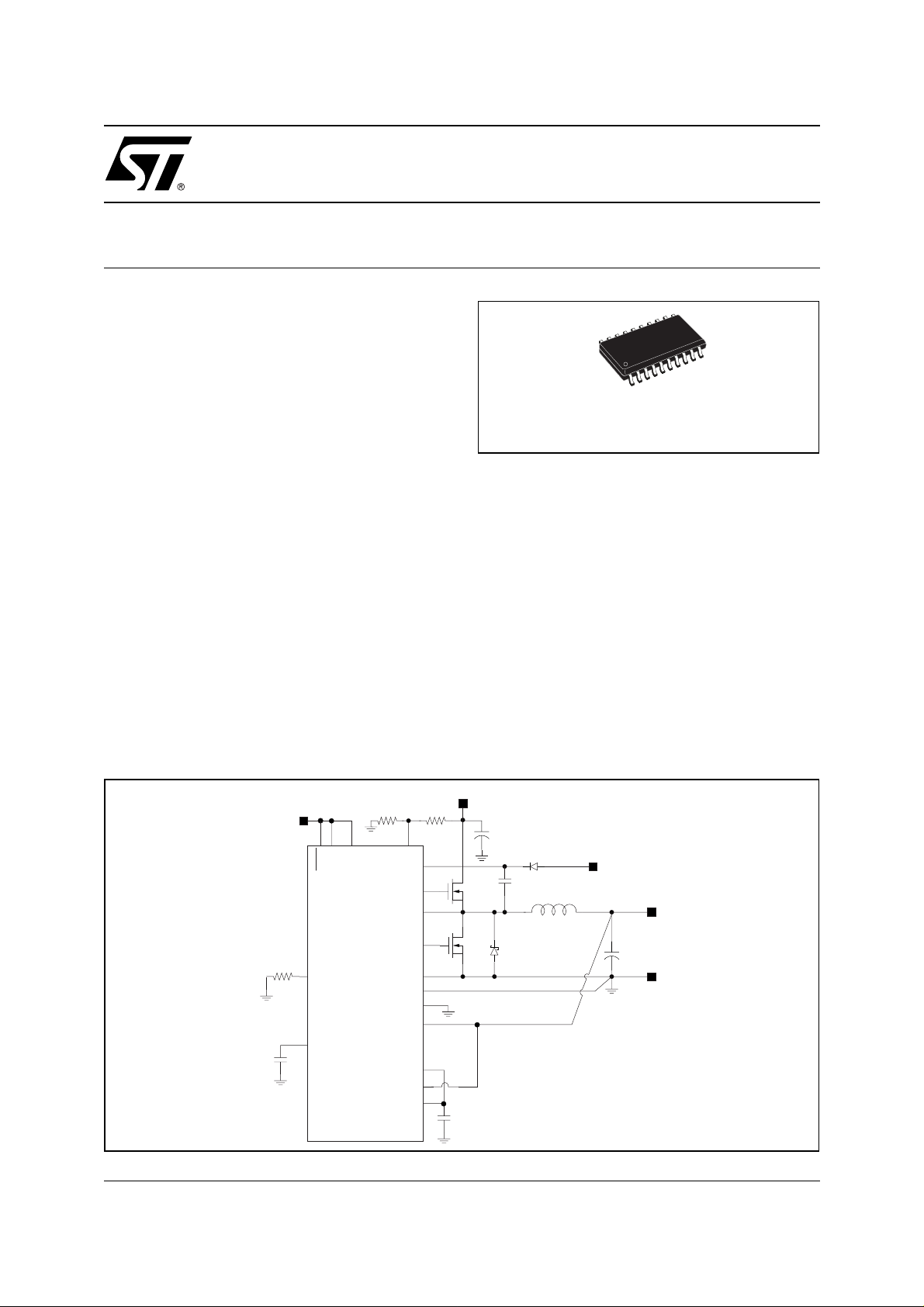
MINIMUM COMPONENT COUNT APPLICATION
Rin2 Rin1
5V
OSC
VDR
VCC
SHDN
RILIM
ILIM
L6995
SS
C
SS
BOOT
HGATE
PHASE
LGATE
PGND
GND
NOSKIP
VSENSE
INT
VFB
VREF
December 2002
This is preliminary information on a new product now in development. Details are subject to change without notice.
28V
C
HS
LS
VREF
CIN
D
BOOT
C
BOOT
L
DS
5V
C
OUT
Vo
0.9V
1/25

L6995
ABSOLUTE MAXIMUM RATINGS
Symbol Parameter Value Unit
V
CC
V
DR
V
PHASE
P
tot
T
stg
THERMAL DATA
Symbol Parameter Value Unit
VCC to GND -0.3 to 6 V
V
to GND -0.3 to 6 V
DR
HGATE and BOOT, to PHASE -0.3 to 6 V
HGATE and BOOT, to PGND -0.3 to 36 V
PHASE -0.3-to 30 V
LGATE to PGND -0.3 to V
ILIM, VFB, VSENSE, NOSKIP, SHDN, PGOOD, OVP, VREF, INT,
SENSE
to GND
= 25°C 1 W
amb
GND
Power dissipation at T
-0.3 to V
+0.3 V
DR
+0.3 V
CC
Storage temperature range -40 to 150 °C
R
th j-amb
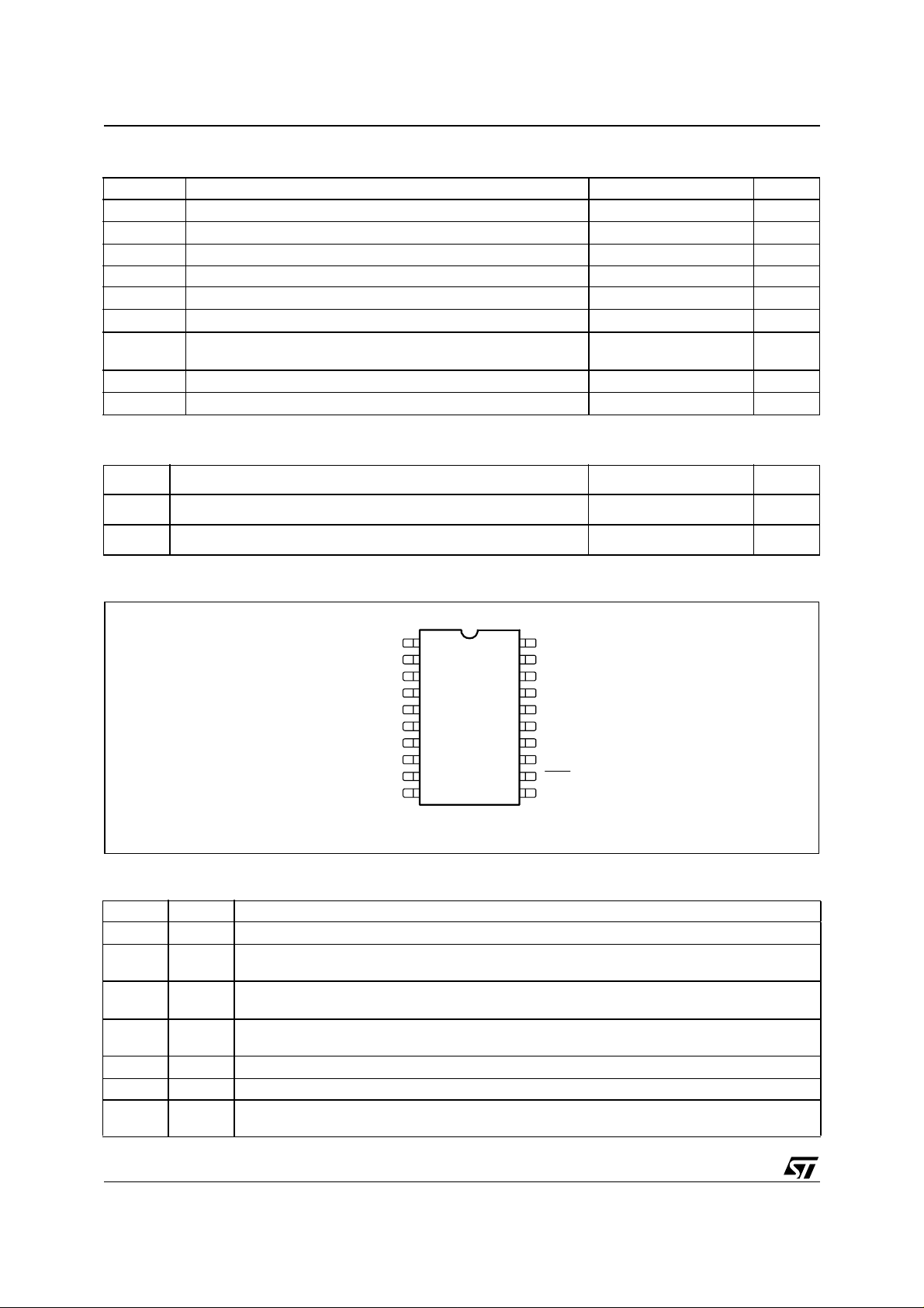
PIN CONNECTION
Thermal Resistance Junction to Ambient 125 °C/W
T
Junction operating temperature range 0 to 125 °C
j
(Top View)
NOSKIP
GNDSENSE
INT
INT
VSENSE
VCC
GND
VREF
VFB
OSC
2
3
4
5
6
7
8
9
10SS
TSSOP20
20
BOOT1
19
HGATE
18
PHASE
17
VDR
16
LGATE
15
PGND
14
PGOOD
13
OVP
12
SHDN
11
ILIM
PIN FUNCTION
N° Name Description
1 NOSKIP Connect to V
2 GNDSE
Remote ground sensing pin
NSE
3 INT Integrator output. Short this pin to VFB pin and connect it via a capacitor to V
integrator in the control loop. If the integrator is not used, short this pin to VREF.
4 VSENSEThis pin must be connected to the remote output voltage to detect overvoltage and undervoltage
conditions and to provide integrator feedback input.
5V
Supply voltage for IC core. Connect to 5V bus.
CC
6 GND Signal ground
7 VREF 0.9 V voltage reference. Connect max. a 10nF ceramic capacitor between this pin and ground.
This pin is capable to source or sink up to 250uA
to force continuous conduction mode and sink mode.
CC
to insert the
OUT
2/25

L6995
PIN FUNCTION
(continued)
N° Name Description
8 VFB PWM comparator feedback input. Short this pin to INT pin when using the integrator function, or
to VSENSE pin without integrator.
9 OSC Connect this pin to the input voltage through a voltage divider in order to provide the feed-
forward function. It cannot be left floating.
10 SS Soft start pin. A 5µA constant current charges an external capacitor which value sets the soft-
start time.
11 ILIM An external resistor connected between this pin and GND sets the current limit threshold.
12 SHDN Shutdown. When shorted to GND the device stops working; when high, it enables the normal
operation. It cannot be left floating.
13 OVP Open drain output. When in OVP condition, the internal transistor goes off. Connect this pin to
V
through a resistor.
CC
14 PGOOD Open drain output. The internal transistor is on during soft-start or in case of output voltage
faults. Connect this pin to V
through a resistor.
CC
15 PGND Low Side driver ground.
16 LGATE Low Side driver output.
17 V
Low Side driver supply.
DR
18 PHASE Return path of the High Side driver.
19 HGATE High side MOSFETS driver output.
20 BOOT Bootstrap capacitor pin. High Side driver is supplied through this pin.
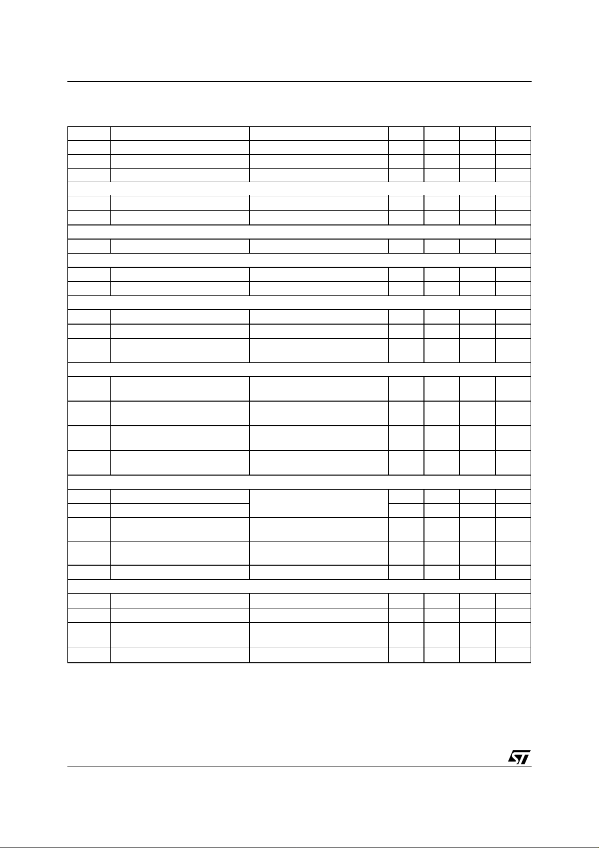
ELECTRICAL CHARACTERISTICS
= VDR = 5V; T
(V
CC
= 0°C to 85°C unless otherwise specified)
amb
Symbol Parameter Test Condition Min. Typ. Max. Unit
SUPPLY SECTION
Vin Input voltage range Vout=Vref Fsw=110Khz Iout=1A 1.5 28 V
V
,
CC
V
DR
V
Turn-onvoltage 4.2 4.4 V
CC
4.5 5.5 V
Tu r n-off voltage 4.1 4.3 V
Iqcc
(V
Iqcc
Driver quiescent current VFB > VREF 20 µA
)
DR
Quiescent current VFB > VREF 600 µA
(Vcc)
SHUTDOWN SECTION
SHDN Device On 1.2 V
Device Off 0.6 V
I
SH
(VDR)
I
SH
Driver quiescent current in
shutdown
Shut down current SHDN to GND 15 µA
SHDN to GND 5 µA
(VCC)
SOFT START SECTION
I
Soft Start current 4 6 µA
SS
SS Clamp Voltage 4 V
ON TIME
Ton On time duration VREF=VSENSE OSC=250mV 850 950 1050 ns
3/25

L6995
ELECTRICAL CHARACTERISTICS
(V
= VDR = 5V; T
CC
= 0°C to 85°C unless otherwise specified)
amb
(continued)
Symbol Parameter Test Condition Min. Typ. Max. Unit
VREF=VSENSE OSC=500mV 380 430 480 ns
VREF=VSENSE OSC=1V 220 250 280 ns
VREF=VSENSE OSC=2V 120 150 180 ns
OFF TIME
T
OFFMIN
Minimum off time 580 ns
K
OSC/TOFFMIN
OSC=250mV 0.4 0.45
VOLTAGE REFERENCE
VREF Voltage Accuracy 0µA < I
< 100µA 0.891 0.9 0.909 V
REF
PWM COMPARATOR
Input voltage offset -2 +2 mV
I
Input Bias Current 0.1 µA
FB
CURRENT LIMIT AND ZERO CURRENT COMPARATOR
K
C
PHASE-
ILIM input bias current I
Current Limit factor R
Zero Crossing Comparator offset -2 2 mV
to GND = 120KΩ 5 µA
LIM
=120 KΩ 0.85 1 1.15 µA
ILIM
GND
GATE DRIVERS
High side rise time V
=5V; C=7nF
DR
50 70 ns
HGATE - PHASE from 2 to 4.5V
High side fall time V
=5V; C=7nF
DR
50 70 ns
HGATE - PHASE from 2 to 4.5V
Low side rise time V
=5V; C=14nF
DR
50 70 ns
LGATE from 2 to 4.5V
Low side fall time V
=5V; C=14nF
DR
50 70 ns
LGATE from 2 to 4.5V
P
UVP/OVP PROTECTIONS
GOOD
OVP Over voltage trip with respect to V
REF
112 115 118 %
UVP Under voltage trip 66 69 72 %
PGOOD Upper threshold
V
rising 107 110 113 %
SENSE
(VSENSE/VREF)
PGOOD Lower threshold
V
falling 86 89 92 %
SENSE
(VSENSE/VREF)
V
PGOOD
I
SOURCE
=2mA 0.14 0.2 V
INTEGRATOR
INT Over Voltage Clamp V
INT Under Voltage Clamp V
-
V
SENSE
V
I
VSENSE
Integrator Input Offset Voltage -5 5 mV
REF
Input Bias Current 0.1 µA
= V
SENSE
SENSE
CC
= GND 0.82 0.84 0.86 V
1.04 1.07 1.1 V
4/25

Figure 1. Funct i on a l & Blo c k D iag ram
IN
V
5V
L6995
OUT
V
GNDVCCOVPPGOODSHDN
overvoltage comparator
VSENSE
+
1.15 VREF
-+undervoltage comparator
VSENSE
0.69 VREF
pgood comparators
SR
LS and HS anti-cross-conduction comparators
1.10 VREF
VSENSE
-
+
comp
V(LGATE)<0.5V
VSENSE
+
BOOT
VCC
0.89 VREF
-
HGATE
HS driver
level shifter
V(PHASE)<0.2V
RQ
comp
S
Toff min
PHASE
delay
VDR
Ton min
one-shot
PGND
LGATE
LS driver
Q
R
S
Ton
one-shot
OSC
VSENSE
Ton= Kosc V(VSENSE)/V(OSC)
Q
R
S
mode
no-skip
-
+
PHASE
zero-cross comparator
LS control
Ton
one-shot
OSC
VSENSE
mode
no-skip
Ton= Kosc V(VSENSE)/V(OSC)
NOSKIP
IC enable
control
soft-start
SS
5 uA
power management
ILIM
comparator
positive current limit
-
PHASE
+-+
+VREF
0.2
FB
HS control
VREF
pwm comparator
+
+
-
-
Gm
VREF
INT
VSENSE
SENSEGND
IN
V
OSC
1.236V
bandgap
VREF
1.416
Reference chain
0.9V
5/25

L6995
1 DEVICE DESCRIPTION
1.1 Constant On Time PWM topology
Figure 2. Loop block schem atic diagr am
Vin
R1
R2
One-shot generator
OSC
Vsense
Vref
FFSR
Q
R
HGATE
S
Q
+
LGATE
HS
LS
Vout
DS
-
PWM comparator
FB
R4
R3
The device implements a Constant On Time control scheme, where the Ton is the high side MOSFET on time
duration forced by the one-shot generator. The on time is directly proportional to VSENSE pin voltage and inverse to OSC pin voltage as in Eq1:
V
SENSE
Eq 1
where K
T
ON
= 250ns and τ is the internal propagation delay time (typ. 70ns). The system imposes in steady
OSC
state a minimum on time corresponding to V
responding Ton will not decrease. Connecting the OSC pin to a voltage partition from V
steady-state switching frequency F
== =
Eq 2
f
SW
K
OSC
V
OUT
-------------- -
V
IN
--------------------- -
V
OSC
1
---------- -
T
ON
τ+=
= 2V. In fact if the V
OSC
independent of VIN. It results:
SW
α
OSC
--------------
α
OUT
1
-------------- -
→ fSWK
K
OSC
α
OSC
OSC
OSCαOUT
voltage increases above 2V the cor-
to G N D, it a l lows a
IN
where
V
Eq 3
Eq 4
α
OSC
α
OUT
OSC
-------------- -
V
IN
V
FB
-------------- -
V
OUT
The above equations allow setting the frequency divide r ratio
such equations hold only if V
independent from the input voltage. The delay introduces a light dependenc e from V
R
2
--------------------==
R2R1+
R
4
--------------------==
R3R4+
α
once output voltage has been set; note that
<2V. Further the Eq2 shows how the system h as a sw itching frequenc y ideall y
OSC
OSC
. A minimum off-time con-
IN
strain of about 580ns is introduced in order to assure the boot capacitor charge and to limit the switching fre-
6/25

L6995
quency after a load transient as well as to mask PWM comparator output against noise and spikes.
The system has not an internal clock, b ecause this is a hysteretic control ler, so the turn on puls e will start if three
conditions are met contemporarily : the FB pin voltage i s low er than the refere nce voltage, the minimum o ff time
is passed and the current limit comparator is not triggered (i.e. the inductor current is below the current limit
value). The voltage on the OSC pin must range between 50mV and 2V to ensure the system linearity.
1.2 Closing the loop
The loop is closed connecting the output voltage (or the output divider middle point) to the FB pin. The FB pin
is linked internally to the comparator negative pin and the positive pin is connected to the reference voltage
(0.9V Typ.) as in Figure 2. When the FB goes lower than the reference voltage, the PWM comparator output
goes high and sets the flip-flop outpu t, turning on the hig h side MOSFET. This condition i s latched to av oid noise
spike. After the on-time (calculated as descr ibed in the previous section) the system resets the flip-flop and then
turns off the high side MOSFET and turns on the low side MOSFET. Internally the device has more complex
logic than a flip-flop to manage the transition in correct way. For more details refers to the Figure 1.
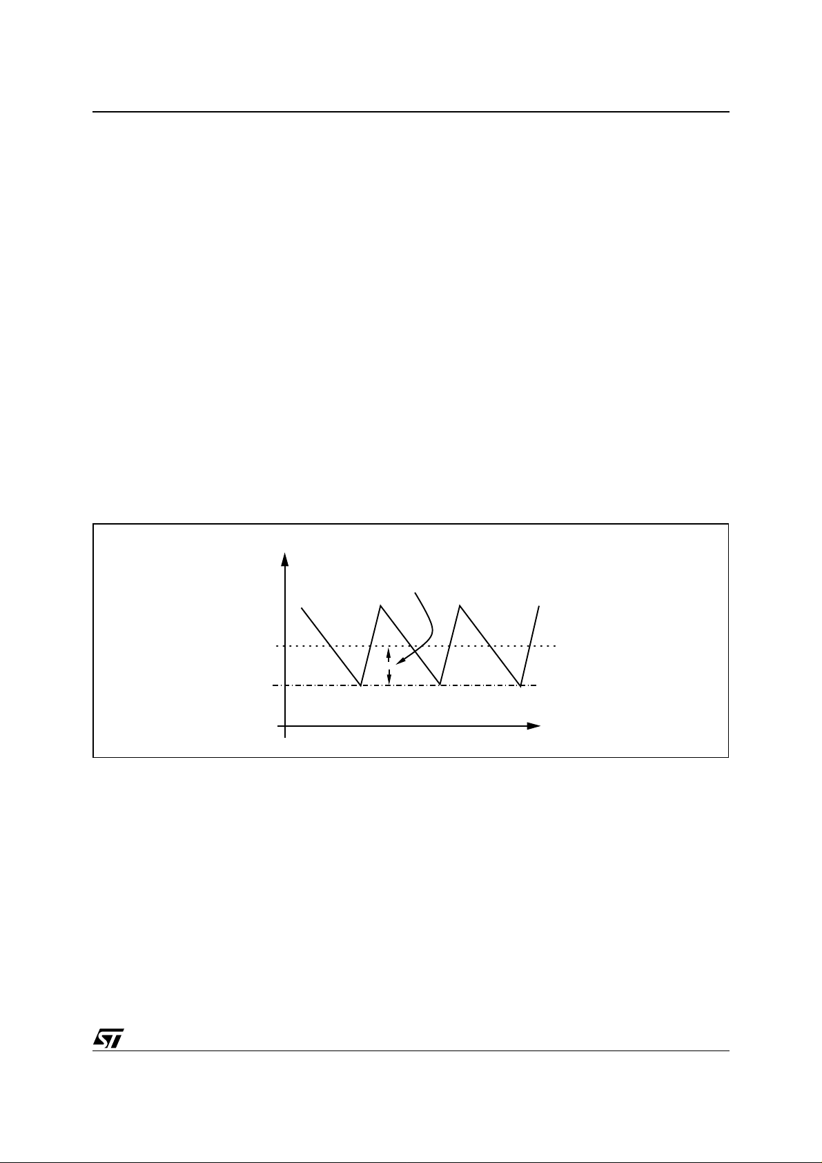
The voltage drop along ground and supply metals connecting output capacitor to the load is a source of DC
error. Further the system r egulates the o utput voltage v alley v alue not the aver age, as in the Fi gure 3 is show n.
So the voltage ripple on the output capacitor is a source of DC static error (as the PCB traces). To compensate
the DC errors, an integrator network must be introduced in the control lo op, by connectin g the output voltage to
the INT pin through a capacitor and the FB pin to the INT pin directly as in Figure 4. The internal integrator amplifier with the exter nal capac itor C
for output ripple.
introduces a D C pole i n the contr ol l oop. C
INT1
also provides an AC path
INT1
Figure 3. Valle y regulation
Vout
DC Error Offset
<Vout>
Vref
Time
The integrator amplifier generates a current, proportional to the DC errors, that increases the output capacitance
voltage in order to c ompensate the total static err ors. A v oltage clamper within the devi ce fo rces INT pi n v oltage
ranges from V
-50mV, V
REF
+150mV. This is useful to avoid or smooth output voltage overshoot during a load
REF
transient. Also, this means that the integrator is capable of recovering output error due to ripple when its peakto-peak amplitude is less than 150mV in steady state.
In case of the ripple amplitude is larger than 150mV, a capacitor C
can be connected between INT pin and
INT2
ground to reduce r ipple amplitu de at INT pin, otherw ise the integrator can operate out of its linear range. Choose
C
according to the following equation:
INT1
g
⋅
INTαOUT
Eq 5
INT1
where GINT=50 µs is the integrator transconductance,
is the close loop bandwidth. This equation also holds if C
--------------------------------- -=
⋅⋅
2 π F
u
α
is the output divider ratio given from Eq4 and F
OUT
is connected between INT pin and ground. C
INT2
INT2
is given by:
U
7/25

L6995
C
Eq 6
Where
INT2
--------------- -
C
INT1
∆
V
is the output ripple and ∆V
OUT
V
∆
OUT
------------------=
V
INT
INT
Figure 4. Integrator loop block diagram
Vin
R1
R2
Cint2
One-shot generator
OSC
From Vsense
Vref
FB
INT
Integrator amplifier
+
-
PWM comparator
+
is the ripple wanted at the INT pin (100mV typ).
PCB TRACES
FFSR
Q
R
HGA TE
S
Q
LGA TE
Vref
-
-
+
Vsense
Gndsense
HS
LS
DS
Vout
LOAD
Cint1
Respect to a traditional PWM controller, that has an internal osci llator setting the sw itchi ng frequency, in a hysteretic system the frequency can change with some parameters (input voltage, output current). In L6995 is implemented the voltage feed-forward circuit that allows constant switching frequency during steady-sate
operation with the input voltage variation. There are many factors affecting switching frequency accuracy in
steady-state operation. Some of these are internal as dead times, which depend on high side MOSFET driver.
Others related to the external components as high side MOSFET gate charge and gate resistance, voltage
drops on supply and ground rails, low side and high side RDSON and inductor parasitic resistance.
During a posi tive load trans ient, (the output current increases), the converter switches at its maxi mum frequency
(the period is TON+TOFFmin) to recover the output voltage drop. During a negative load transient, (the output
current decreases), the device stops to switch (high side MOSFET remains off).
1.3 Tran si t ion from PWM to PFM/PSK
To achieve high efficiency at light load condition s, PFM mode is provided. The PFM mode differs from the PWM
mode essentially for the off section; the on section is the same. In PFM after a turn-on cycle the system turnson the low side MOSFET, until the inductor current reaches the zero A value, when the zero-crossing comparator turns off the low side M OSFET. In this w ay the energy stor ed in the outp ut capaci tor wi ll not flow to gr ound,
through the low side MO SFET, but it w ill flow to the load. In PWM mode, after a turn on cy cle, the sy stem k eeps
the low side MOSFET on until the next turn-on cycle, so the energy stored in the output capacitor will flow
through the low side MOSFET to ground. The PFM mode is naturally implemented in hysteretic controller, in
fact in PFM mode the system reads the output vol tage with a comparator and then tur ns on the hig h side MOSFET when the output voltage goes down a reference value. The device works in discontinuous mode at light
load and in continu ous mode at high l oad. The transi tion fr om PFM to PWM oc curs when load current is around
half the inductor current ripple. This threshold value depends on V
, L, and V
IN
. Note that the higher the in-
OUT
8/25
 Loading...