

HIGH PERFORMANCE 2A ULDO LINEAR REGULATOR
■ 2V TO 14V INPUT VOLTAGE RANGE
■ 200mΩ Rdson MAX.
■ 200µA QUIESCENT CURRENT AT ANY LOAD
■ EXCELLENT LOAD AND LINE REGULATION
■ 1.8V AND 2.5V FIXED VOLTAGE
■ ADJUSTABLE FROM 1.2V TO 5V (L6932D1.2)
■ 1% VOLTAGE REGULATION ACCURACY
■ SHORT CIRCUIT PROTECTION
■ THERMAL SHUT DOW N
■ SO-8 (4+4) PACKAGE
APPLICATIONS
■ MOTHERBOARDS
■ MOBILE PC
■ HAND-HELD INSTRUMENTS
■ PCMCIA CARDS
■ PROCESSORS I/O
■ CHIPSET AND RAM SUPPLY
DESCRIPTION
The L6932 Ultra Low Drop Output linear regulator operates from 2V to 14V and is able to su pport 2A. Designed with an internal 50m
Ω
N-channel
L6932
SO-8 (4+4)
ORDERING NUMBERS:
L6932D1.2 (SO-8 ) L6932D1.2TR (T&R)
L6932D1.8 (SO-8 ) L6932D1.8TR (T&R)
L6932D2.5 (SO-8 ) L6932D2.5TR (T&R)
Mosfet, can be usefull for the DC-DC conversion between 2.5V and 1.8V at 2A in portable applications
reducing the power dissipation.
L6932 is available in 1.8V, 2.5V and adj version from
1.2V and ensure a voltage regulation accuracy of
1%.
The current limit is fix ed at 2.5A to contr ol the current
in short circuit condition within ±8%. The current is
sensed in the power mos in order to limit the power
dissipation.
The device is also provided of a thermal shut down
that limits the internal temperature at 150°C with an
histeresys of 20°C. L6932 provides the Enable and
the Power good functions.
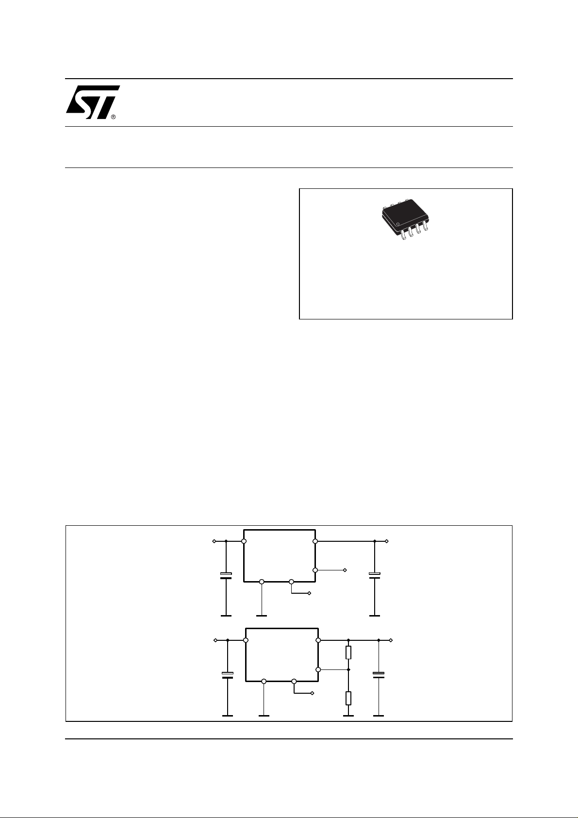
TYPICAL OPERATING CIRCUIT
VIN
2V to 14V
VIN
2V to 14V
February 2003
IN
2
L6932D
C1 C2
5,6,7,8
IN
2
1
GND
L6932D1.2
C1
5,6,7,8
1
GND
EN
EN
OUT
3
PGOOD
4
OUT
4
ADJ
3
1.8V or 2.5V
R1
R2
VOUT
VOUT
1.2V to 5V
C2
1/10
L6932
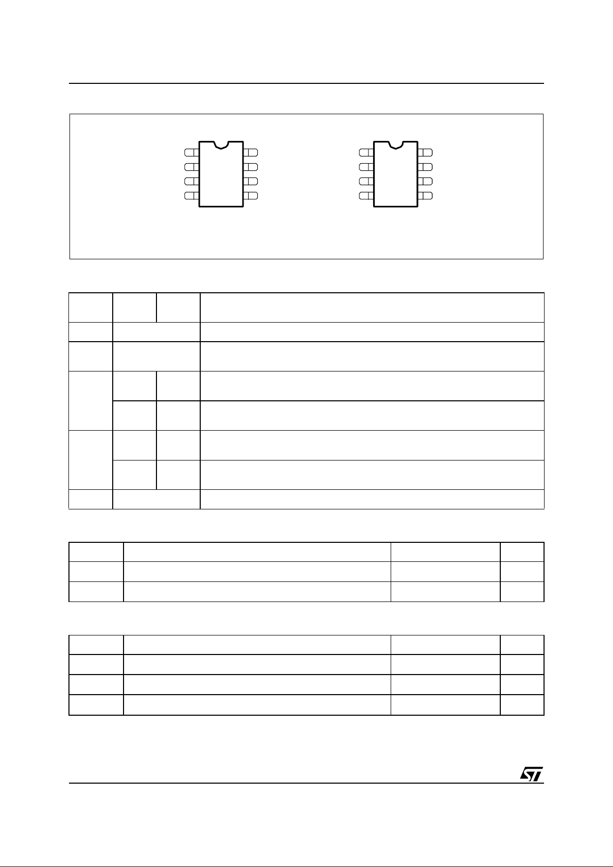
PIN CONNECTIONS
EN
IN
ADJ
OUT 5
1
2
3
4
L6932D1.2
8
7
6
GND
GND
GND
GND
EN
IN
OUT
PGOOD 5
1
2
3
4
L6932D1.8
L6932D2.5
8
7
6
GND
GND
GND
GND
PIN FUNCTION
N°
L6232D
1.2
1 EN Enables the device if connected to Vin and disables the device if forced to gnd.
2 IN Supply voltage. This pin is connected to the drain of the internal N-mos. Connect this
ADJ – Connecting this pin to a voltage divider it is possible to programme the output voltage
3
OUT – Regulated output voltage. This pin is connected to the source of the internal N-mos.
4
L6232D
1.8/2.5
Description
pin to a capacitor larger than 10µF.
between 1.2V and 5V.
– OUT Regulated output voltage. This pin is connected to the source of the internal N-mos.
Connect this pin to a capacitor of 10µF.
Connect this pin to a capacitor of 10µF.
– PGOOD Power good output. The pin is open drain and detects the output voltage. It is forced
low if the output voltage is lower than 90% of the programmed voltage.
5, 6, 7, 8 GND Ground pin.
ABSOLUTE MAXIMUM RATINGS
Symbol Parameter Value Unit
V
in
VIN and Pgood 14.5 V
EN, OUT and ADJ -0.3 to (Vin +0.3) V
THERMAL DATA
Symbol Parameter Value Unit
R
th J-amb
T
max
T
stg
(*) Measured on Demoboard with about 4 cm2 of dissipating area 2 Oz.
2/10
Thermal Resistance Junction to Ambient 62 (*) °C/W
Maximum Junction Temperature 150 °C
Storage Temperature Range -65 to 150 °C

L6932
BLOCK DIAGRAM
GND
ELECTRICAL CHARACTERISTCS
(*) Specification referred to T
(Referred to the Fixed Voltage version)
IN
REFERENCE
VREF=1.25V
ENABLEEN
THERMAL
SENSOR
(Tj = 25°C, VIN = 5V unless otherwise specified)
from -25°C to 125°C.
j
VREF
0.9 VREF
+
ERROR
AMPL.
CHARGE
PUMP
+
CURRENT
LIMIT
DRIVER
OUT
PG
D99IN1100
Symbol Parameter Test Condition Min. Typ. Max. Unit
V
V
R
I
I
V
Operating Supply Voltage 2 14 V
in
Output voltage L6932D1.2 Io = 0.1A; Vin = 3.3V 1.188 1.2 1.212 V
o
Output voltage L6932D1.8 I
Output voltage L6932D2.5 I
L6932D1.2
Line Regulation
L6932D1.8
Line Regulation
L6932D2.5
Line Regulation
L6932D1.2 Load Regulation V
L6932D1.8 Load Regulation V
L6932D2.5 Load Regulation V
Drain Source ON resistance 200 mΩ
dson
Current limiting 2.3 2.5 2.7 A
occ
Quiescent current 0.2 0. 4 mA
I
q
Shutdown current 2V < Vin < 14V
sh
Ripple Rejection f = 120Hz, I
EN Input Threshold 0.5 0.65 0.8 V
en
= 0.1A; Vin = 3.3V 1.782 1.8 1.818 V
o
= 0.1A; Vin = 3.3V 2.475 2.5 2.525 V
o
V
= 2.5V ±10%; Io = 10mA 5 mV
in
= 3.3V ±10%; Io = 10mA 5 mV
V
in
= 5V ±10%; Io = 10mA 5 mV
V
in
V
= 2.5V ±10%; Io = 10mA 5 mV
in
= 3.3V ±10%; Io = 10mA 5 mV
V
in
= 5V ±10%; Io = 10mA 5 mV
V
in
V
= 3.3V ±10%; Io = 10mA 5 mV
in
= 5V ±10%; Io = 10mA 5 mV
V
in
= 3.3V; 0.1A < Io < 2A 15 mV
in
= 3.3V; 0.1A < Io < 2A 15 mV
in
= 3.3V; 0.1A < Io < 2A 15 mV
in
*
= 1A
V
= 5V, ∆Vin = 2Vpp
in
o
60 75 dB
25 µA
3/10

L6932
ELECTRICAL CHARACTERISTCS
(continued)
Symbol Parameter Test Condition Min. Typ. Max. Unit
Pgood threshold Vo rise 90 %Vo
Pgood Hysteresis 10 %Vo
Pgood saturation I
Figure 1. Out put V ol t age v s. Junction
Temperature (L6932D1.2)
1.213
1.212
1.212
1.211
V
1.211
1.210
1.210
1.209
-60 -40 -20 0 20 40 60 80 100 120 140 160
Temp [°C]
Figure 2. Out put V ol t age v s. Junction
Temperature (L6932D1.8)
=1mA 0.2 0.4 V
pgood
Figure 4. Quiescent Current vs. Junction
Temperature
310
300
Vin=5V
290
Iq
280
(uA)
270
260
250
-40 -20 0 20 40 60 80 100 120 140
Temp [°C ]
Figure 5. Shutdown Curr ent v s. Junc ti on
Temperature
1.808
1.804
1.800
V
1.796
1.792
1.788
-60 -40 -20 0 20 40 60 80 100 120 140 160
Temp [°C]
Figure 3. Out put V ol t age v s. Junction
Temperature (L6932D2.5)
2.520
2.515
2.510
V
2.505
2.500
7.5
7
6.5
Ishdn
(uA)
Vin=5V
6
5.5
5
4.5
4
-40 -20 0 20 40 60 80 100 120 140
Temp [°C ]
4/10
2.495
-60 -40 -20 0 20 40 60 80 100 120 140 160
Temp [°C]

APPLICATION INFORMATIONS
APPLICATION CIRCUIT
In figure 6 the schematic circuit of the demoboards are shown.
Figure 6. Dem ob oards Schem atic Circui t
L6932
VIN
IN
2
OUT
3
VOUT=2.5V/1.8V
L6932D2.5
VIN
EN
C1
IN
2
1
5
L6932D1.2
6
GND
7
EN
C1
4
3
8
1
5
GND
OUT
ADJ
L6932D1.8
6
VOUT=1.2V TO 5V
R1
R2
PGOOD
4
8
7
C2
V
C2
OUT
1.2
------- -
R2
COMPONENT LIST
Fixed version
Reference Part Number Description Manufacturer
R1 R2+()⋅=
C1 C34Y5U1E106Z 10uF, 25V TOKIN
C2 C34Y5U1E106Z 10uF, 25V TOKIN
Figure 7. Demoboard Lay out (Fi xe d Versi on)
5/10

L6932
Adjustable version
Reference Part Number Description Manufacturer
C1 C34Y5U1E106Z 10uF, 25V TOKIN
C2 C34Y5U1E106Z 10uF, 25V TOKIN
R1 5.6K, 1%, 0.25W Neohm
R2 3.3K, 1%, 0.25W Neohm
Figure 8. Dem ob oard Layout (A dj ust able Versio n)
COMPONENTS SELECTION
Input Capacitor
The input capacitor value depends on a lot of facto rs such as load transient r equi rements, input s ource ( battery
or DC/DC converter) and its distance from the input cap. Usually a 47
µ
F is enough for any application but a
much lower value can be sufficient in many cases.
Output Capacitor
The output capacitor choice depends basically on the load transient requirements.
Tantalum, Speciality Polimer, POSCAP and aluminum capacitors are good and offer very low ESR values.
Multilayer ceramic caps have the lowest ESR and can be r equired for particular applications. Nevertheless in
several applications they are ok, the loop stability issue has to be considered (see loop stability section).
Below a list of some suggested capacitor manufacturers.
Manufacturer Type Cap Value (µF) Rated Voltage (V)
PANASONIC CERAMIC 1 to 47 4 to 16
TAYO YUDEN CERAMIC 1 to 47 4 to 16
TDK CERAMIC 1 to 47 4 to 16
TOKIN CERAMIC 1 to 47 4 to 16
SANYO POSCAP 1 to 47 4 to 16
PANASONIC SP 1 to 47 4 to 16
KEMET TANTALUM 1 to 47 4 to 16
6/10

Loop Stability
The stability of the loop is affected by the zero introduced by the output capacitor.
The time constant of the zero is given by:
L6932
T ESR C
⋅= F
OUT
ZERO
--------------------------------------------=
2π ESR C
1
⋅⋅
OUT
This zero helps to increase the phase margin of the loop until the time constant is higher than some hundreds
of nsec, depending also on the output voltage and current.
So, using very low ESR ceramic capaci tors could produce oscillations at the output, in particular when regul ating
high output voltages (adjustable version).
To solve this issue is sufficient to add a small capacitor (e.g. 1nF to 10nF) in parallel to the high side resistor of
the external divider, as shown in figure 9.
Figure 9. Comp e nsation Network
VIN=2V TO 14V
C1
IN
EN
2
1
5
L6932D1.2
6
GND
OUT
4
R1
ADJ
3
8
7
R2
VOUT=1.2V TO 5V UP to 2A
C3
C2
Thermal Considerations
Since the device is housed in a small SO(4+2+2) package the thermal issue can be the bottleneck of many applications. The power dissipated by the device is given by:
P
DISS
= (VIN - V
OUT
) · I
OUT
The thermal resistance junction to ambient of the demoboard is approximately 62°C/W. This mean that, considering an ambient temperature of 60°C and a maximum junction temperature of 150°C, the maximum power that
the device can handle is 1.5W.
This means that the device is able to deliver a DC output current of 2A only with a very low dropout.
In many applications, high output current pulses are required. If their duration is shorter than the thermal con-
stant time of the board, the thermal impedance (not the thermal resistance) has to be considered.
In figure 10 the thermal impedance versus the duration of the current pulse for the SO(4+2+2) mounted on board
is shown.
7/10

L6932
Figure 10. Thermal Impedance
Considering a pulse duration of 1sec, the thermal impedance is close to 20°C/W, allowing much bigger power
dissipated.
Example:
Vin = 3.3V
Vout = 1.8V
Iout = 2A
Pulse Duration = 1sec
The power dissipated by the device is:
P
DISS
= (VIN - V
OUT
) · I
OUT
= 1.5 · 2 3W
Considering a thermal impedance of 20°C/W, the maximum junction temperature will be:
= TA + Z
T
J
THJA
· P
= 60 + 60 = 120°C
DISS
Obviously, with pulse durations longer than approximately 10sec the thermal impedance is very close to the
thermal resistance (60°C/W to 70°C/W).
8/10
L6932
DIM.
D (1) 4.8 5.0 0.189 0.197
F (1) 3.8 4.0 0.15 0.157
(1) D and F do not include mold flash or protrusions. Mold flash or
potrusions shall not exceed 0.15mm (.006inch).
MIN. TYP. MAX. MIN. TYP. MAX.
A 1.75 0.069
a1 0.1 0.25 0.004 0.010
a2 1.65 0.065
a3 0.65 0.85 0.026 0.033
b 0.35 0.48 0.014 0.019
b1 0.19 0.25 0.007 0.010
C 0.25 0.5 0.010 0.020
c1 45° (typ.)
E 5.8 6.2 0.228 0.244
e 1.27 0.050
e3 3.81 0.150
L 0.4 1.27 0.016 0.050
M 0.6 0.024
S8° (max.)
mm inch
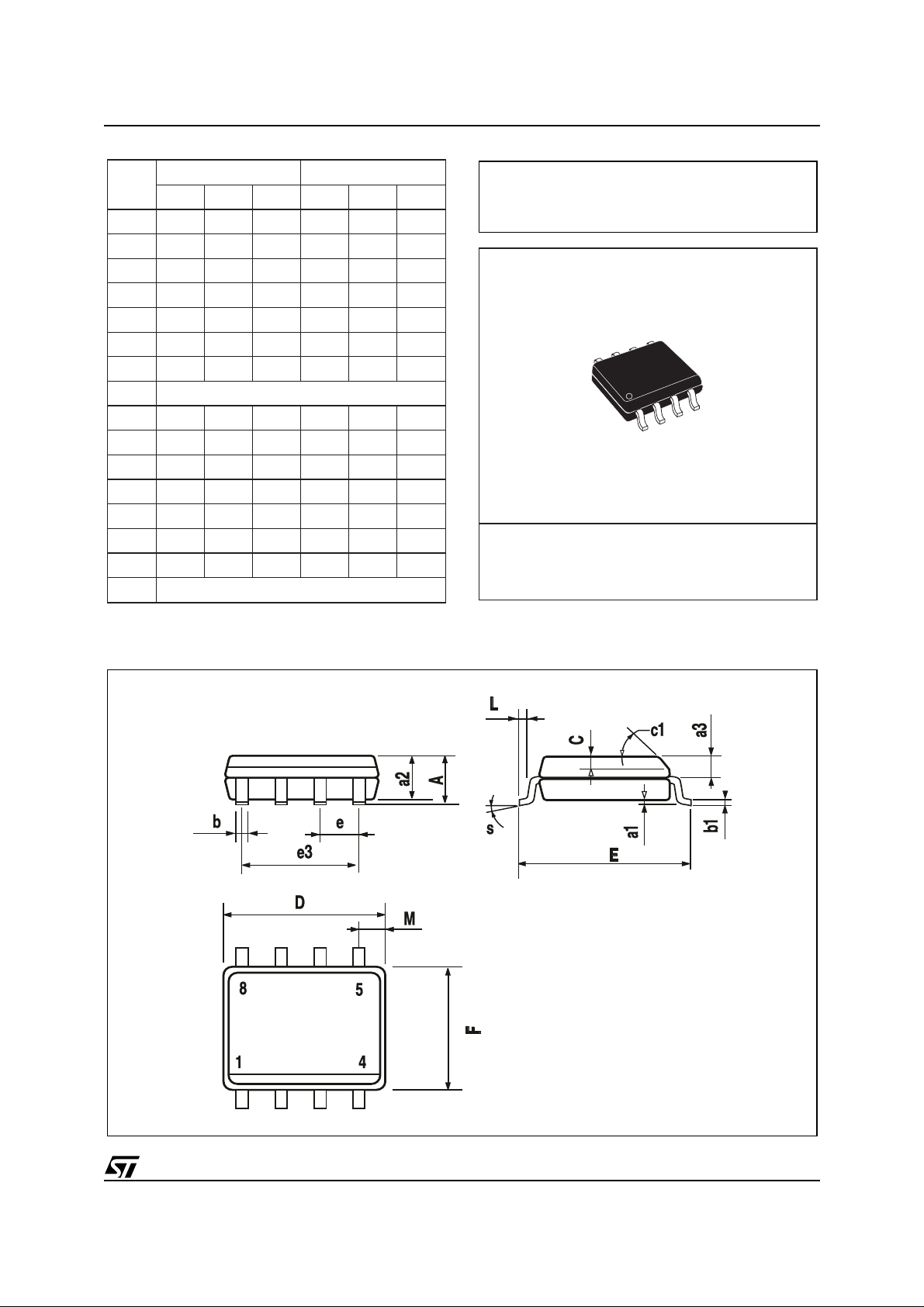
OUTLINE AND
MECHANICAL DATA
SO8
9/10

L6932
Information furnishe d is believed to be accur ate and reliable. Howe ver , STMicroele ctro nics as sumes no responsib ility for the consequences
of use of such information nor for any infringement of patents or other rights of third parties which may result from its use. No license is granted
by implication or otherwise under any patent or patent rights of STMicroelectronics. Sp ecifications ment ioned in this publication are subject
to change without notice. This publication supersedes and replaces all information previously supplied. STMicroelectronics products are not
authorized for use as critical components in life support devices or systems without express written approval of STMicroelectronics.
The ST logo is a registered trademark of STMicroelectronics
2003 STMicroelectronics - All Rights Reserved
Austra lia - Brazil - Canada - Chi na - Finland - France - Germany - Hong Kong - India - Isr ael - Italy - Japan -Malaysia - Malta - Morocco -
Singap ore - Spain - Sw eden - Switze rland - United Kingdom - United States.
STMicroelectronics GROUP OF COMPANIES
http://www.s t. com
10/10
 Loading...