


5 BIT PROGRAMMABLE DUAL-PHASE CONTROLLER
WITH DYNAMIC VID MANAGEMENT
■
2 PHASE OPERATION WITH
SYNCRHONOUS RECTIFIER CONTROL
■
ULTRA FAST LOAD TRANSIENT RESPONSE
■
INTEGRATED HIGH CURRENT GATE
DRIVERS: UP TO 2A GATE CURRENT
■
TTL-COMP A T I BLE 5 BIT P ROGR AMMABLE
OUTPUT FROM 0.800V TO 1.550V WITH
25mV STEPS
■
DYNAMIC VID MANAGEMENT
■
0.6% OUTPUT VOLTAGE ACCURACY
■
10% ACTIVE CURRENT SHARIN G ACCURACY
■
DIGITAL 2048 STEP SOFT-START
■
OVERVOLTAGE PROTEC T I O N
■
OVERCURRENT PROTECTION REALIZED
USING THE LOWER MOSFET'S R
SENSE RESISTOR
■
OSCILLATOR EXTERNALLY ADJUST ABLE
AND INTERNALLY FIXED AT 200kHz
■
POWER GOOD OUTPUT AND INHIBIT
FUNCTI ON
■
REMOTE SENSE BUFFER
■
PACKAGE: SO-28
APPLICATION S
■
POWER SUPPLY FOR SERVERS AND
WORKSTATIONS
■
POWER SUPPLY FOR HIGH CURRENT
MICROPROCESSORS
■
DISTRIBUTED PO WE R SUPP LY
dsON
OR A
L6919C
SO-28
ORDERING NUMBERS:L6919CD
L6919CDTR
DESCRIPTION
The device is a power supply controller specifically designed to provide a high performance DC/DC conversion for high current microprocessors. The device
implements a dual-phase step-down controller with a
180° phase-shift between each phase. A precise 5-bit
digital to analog converter (DAC) allows adjusting the
output volt age from 0.800V to 1.550V with 25mV binary
steps managi ng O n-The-Fly VID code changes.
The high precision internal r eference ass ures the selected output voltage to be within ±0.6%. The high
peak current gate drive affor ds to hav e fast s witching
to the external power mos providing low switching
losses.
The device assures a fast protection against load
over current and load over/under vol t age. An internal
crowbar is provided turning on the low side mosfet if
an over-voltage is detected. In case of over-current,
the system works in Constant Current mode.
BLOCK DIAGRAM
PGOOD
PGOOD
December 2002
VID4
VID4
VID3
VID3
VID2
VID2
VID1
VID1
VID0
VID0
FBG
FBG
FBR
FBR
DIGITAL
DIGITAL
SOF T- S TAR T
SOF T- S TAR T
DAC
DAC
32k
32k
32k
32k
32k
32k
32k
32k
REMOTE
REMOTE
BUFFE R
BUFFE R
OSC / INH SGND VCCDR
OSC / INH SGND VCCDR
PWM1
TO TA L
TO TA L
CURRENT
CURRENT
CURRENT
CURRENT
PWM1
AVG
AVG
PWM2
PWM2
LOGIC PWM
LOGIC PWM
LOGIC PWM
ADAPTIVE ANTI
ADAPTIVE ANTI
CH1
CH1
OCP
OCP
CURRENT
CURRENT
CORRECTION
CORRECTION
CH2
CH2
OCP
OCP
CURRENT
CURRENT
CORRECTION
CORRECTION
ADAPTIVE ANTI
CRO SS C OND U CT ION
CRO SS C OND U CT ION
CRO SS C OND U CT ION
CURRENT
CURREN T
CURREN T
READING
READING
READING
CURREN T
CURREN T
CURREN T
READING
READING
READING
LOGIC PWM
LOGIC PWM
LOGIC PWM
ADAPTIVE ANTI
ADAPTIVE ANTI
ADAPTIVE ANTI
CROSS CONDUCTION
CROSS CONDUCTION
CROSS CONDUCTION
Vcc
Vcc
VccCOM PFBVSEN
VccCOM PFBVSEN
I
I
FB
FB
2 PH AS E
2 PH AS E
LOGIC AND
LOGIC AND
CH1 OCP
CH1 OCP
OSCILLATOR
OSCILLATOR
PROTECTIONS
PROTECTIONS
CH2 OCP
CH2 OCP
VCC
VCC
VCCDR
VCCDR
ERROR
ERROR
A MPLIF IER
A MPLIF IER
BOO T 1
BOO T 1
HS
HS
LS
LS
LS
LS
HS
HS
U
U
GA T E 1
GA T E 1
PHASE1
PHASE1
LGATE1
LGATE1
ISEN1
ISEN1
PGNDS1
PGNDS1
PGND
PGND
PGNDS2
PGNDS2
ISEN2
ISEN2
LGATE2
LGATE2
PHASE2
PHASE2
UGATE2
UGATE2
BOO T 2
BOO T 2
1/32
L6919C
ABSOLUTE MAXIMUM RATINGS
Symbol Parameter Value Unit
Vcc, V
CCDR
V
BOOT-VPHASE
V
UGATE1-VPHASE1
V
UGATE2-VPHASE2
V
phase
THERMAL DATA
Symbol Parameter Value Unit
to PGND 15 V
Boot Voltage 15 V
15 V
LGATE1, PHASE1, LGATE2, PHASE2 to PGND -0.3 to Vcc+0.3 V
VID0 to VID4 -0.3 to 5 V
All other pins to PGND -0.3 to 7 V
Sustainable Peak Voltage t < 20ns @ 600kHz 26 V
R
th j-amb
T
T
storage
P
Thermal Resistance Junction to Ambient 60 °C/W
Maximum junction temperature 150 °C
max
Storage temperature range -40 to 150 °C
T
Junction Temperature Range 0 to 125 °C
j
Max power dissipation at T
MAX
PIN CONNECTION
LGATE1
VCCDR
PHASE1
UGATE1
BOOT1
VCC
SGND
COMP
FB
VSEN
FBR
FBG
ISEN1
PGNDS1
= 25°C 2 W
amb
1
2
3
4
5
6
7
8
9
10
11
12
13
14
L6919C
28
27
26
25
24
23
22
21
20
19
18
17
16
15
PGND
LGATE2
PHASE2
UGATE2
BOOT2
PGOOD
VID4
VID3
VID2
VID1
VID0
OSC / INH / FAULT
ISEN2
PGNDS2
2/32

L6919C
ELECTRICAL CHARACTERISTICS
= 12V
V
CC
Symbol Parameter Test Condition Min Typ Max Unit
Vcc SUPPLY CURRENT
±10%
, TJ = 0 to 70°C unless otherwise specified
I
CC
I
CCDR
I
BOOTx
Vcc supply current HGATEx and LGATEx open
V
V
supply current LGATEx open; V
CCDR
CCDR=VBOOT
=12V
=12V 2 3 4 mA
CCDR
Boot supply current HGATEx open; PHASEx to PGND
V
CC=VBOOT
=12V
7.5 10 12.5 mA
0.5 1 1.5 mA
POWER-ON
Turn-On V
Turn-Off V
Turn-On V
Threshold
Turn-Off V
Threshold
threshold VCC Rising; V
CC
threshold VCC Falling; V
CC
V
CCDR
CCDR
Rising
VCC=12V
V
CCDR
CCDR
Falling
VCC=12V
=5V 8 9.2 10.4 V
CCDR
=5V 6.5 7.5 8.5 V
CCDR
4.2 4.4 4.6 V
4.0 4.2 4.4 V
OSCILLATOR/INHIBIT/FAULT
f
OSC
f
OSC,Rosc
INH Inhibit threshold I
d
Initial Accuracy OSC = OPEN
OSC = OPEN; Tj=0°C to 125°C
185
180
200 215
Total Accuracy RT to GND=74kΩ 360 400 440 kHz
=5mA 0.5 V
SINK
Maximum duty cycle OSC = OPEN; IFB = 0 75 80 %
MAX
OSC = OPEN; I
= 60µA3846 %
FB
220
∆Vosc Ramp Amplitude 1.8 2 2.2 V
kHz
kHz
FAULT Voltage at pin OSC OVP or UVP Active 4.75 5.0 5.25 V
REFERENCE AND DAC
-0.6 - 0.6 %
I
DAC
Output Voltage
Accuracy
VID0, VID1, VID2, VID3, VID4
see Table1;
FBR = V
; FBG = GND
OUT
VID pull-up Current VIDx = GND 4 5 6 µA
VID pull-up Voltage VIDx = OPEN 3.2 - 3.5 V
ERROR AMPLIFIER
DC Gain 80 dB
SR Slew-Rate COMP=10pF 15 V/µs
DIFFERENTIAL AMPLIFIER (REMOTE BUFFER)
DC Gain 1 V/V
CMRR Common Mode Rejection Ratio 40 dB
SR Slew Rate VSEN=10pF 15 V/µs
3/32

L6919C
ELECTRICAL CHARACTERISTICS
V
= 12V
CC
±10%
, TJ = 0 to 70°C unless otherwise specified
(continued)
Symbol Parameter Test Condition Min Typ Max Unit
DIFFERENTIAL CURRENT SENSING
,
I
ISEN1
I
ISEN2
I
PGNDSx
I
ISEN1
I
ISEN2
I
FB
Bias Current I
Bias Current 45 50 55 µA
,
Bias Current at
Over Current Threshold
Active Droop Current I
= 0 45 50 55 µA
LOAD
80 85 90 µA
LOAD
I
LOAD
≤ 0%
= 100%
47.5
0
50
1
52.5
GATE DRIVERS
t
RISE
HGATE
I
HGATEx
High Side
Rise Time
High Side
V
BOOTx-VPHASEx
C
V
to PHASEx=3.3nF
HGATEx
BOOTx-VPHASEx
=10V;
15 30 ns
=10V 2 A
Source Current
R
HGATEx
High Side
V
BOOTx-VPHASEx
=12V; 1.5 2 2.5 Ω
Sink Resistance
t
RISE
LGATE
I
LGATEx
Low Side
Rise Time
Low Side
V
=10V;
CCDR
C
V
to PGNDx=5.6nF
LGATEx
=10V 1.8 A
CCDR
30 55 ns
Source Current
µA
µA
R
LGATEx
Low Side
Sink Resistance
PROTECTIONS
PGOOD Upper Threshold
(V
/DAC Output)
SEN
PGOOD Lower Threshold
/DAC Output)
(V
SEN
OVP Over Voltage Threshold
)
(V
SEN
UVP Under Voltage Trip
/DAC Output)
(V
SEN
V
PGOOD
PGOOD Voltage Low I
V
=12V 0.7 1.1 1.5 Ω
CCDR
V
Rising 108 112 116 %
SEN
V
Falling 84 88 92 %
SEN
V
Rising 1.915 2.05 V
SEN
V
Falling 65 70 75 %
SEN
= -4mA 0.3 0.4 0.5 V
PGOOD
4/32
Table 1. Voltage Identification (VID) Codes
VID4 VID3 VID2 VID1 VID0
00000
00001
00010
00011
00100
00101
00110
00111
01000
01001
01010
01011
01100
01101
01110
01111
Output
Voltage (V)
1.550
1.525
1.500
1.475
1.450
1.425
1.400
1.375
1.350
1.325
1.300
1.275
1.250
1.225
1.200
1.175
VID4 VID3 VID2 VID1 VID0
10000
10001
10010
10011
10100
10101
10110
10111
11000
11001
11010
11011
11100
11101
11110
11111
L6919C
Output
Voltage (V)
1.150
1.125
1.100
1.075
1.050
1.025
1.000
0.975
0.950
0.925
0.900
0.875
0.850
0.825
0.800
Shutdown
Reference Schematic
Vin
GNDin
L1
S4
S3
S2
S1
S0
HS1
LS1
C
IN
VCCDR
2
BOOT1
5
UGATE1
4
PHASE1
3
LGATE1
1
ISEN1
PGNDS1
OSC / IN H
SGND
VID4
VID3
VID2
VID1
VID0
13
14
L6919C
22
21
20
19
18
17
7
11 12
FBR FBG
Rg
Rg
VCC
6
BOOT2
24
UGATE2
25
PHASE2
26
LGATE2
27
ISEN2
16
PGNDS2
15
PGND
28
PGOOD
23
VSEN
10
FB
9
COMP
8
HS2
L2
C
LS2
Rg
Rg
R
FB
R
F
C
F
OUT
LOAD
PGOOD
5/32

L6919C
PIN FUNCTION
N Name Description
1 LGATE1 Channel 1 low side gate driver output.
2 VCCDR LS Mosfet driver supply. It can be varied from 5V to 12V.
3 PHASE1 This pin is connected to the source of the upper mosfet and provides the return path for the high
4 UGATE1 Channel 1 high side gate driver output.
5 BOOT1 Channel 1 bootstrap capacitor pin. Through this pin is supplied the high side driver and the upper
6 VCC Device supply voltage. The operative supply voltage is 12V.
7 GND All the internal references are referred to this pin. Connect it to the PCB signal ground.
8 COMP This pin is connected to the error amplifier output and is used to compensate the control
9 FB This pin is connected to the error amplifier inverting input and is used to compensate the voltage
10 VS EN Connected to the outpu t voltage it is able to manage Over&Unde r-voltage conditions and the
11 FBR Remote sense buffer non-inverting input. It has to be connected to the positive side of the load to
side driver of channel 1.
mosfet. Connect through a capacitor to the PHASE1 pin and through a diode to Vcc (cathode vs.
boot).
feedback loop.
control feedback loop.
A current prop ortional to t he su m of the c urren t sen sed i n bot h cha nnel is so urced from this pin
(50µA at full load, 70µA at the 140% Constant Current threshold). Connecting a resistor between
this pin and VSEN pin allows programming the droop effect.
PGOOD signal. It is internally connected with the output of the Remote Sense Buffer for Remote
Sense of the regulated voltage.
If no Remote Sense is implemented, connect it directly to the regulated voltage in order to
manage OVP, UVP and PGOOD.
perform a remote sense.
If no remote sense is implemen ted, conn ect directl y to the output voltage (in this c ase conn ect
also the VSEN pin directly to the output regulated voltage).
12 FBG Remote se nse buffer inverting input. It has to b e connected to the ne gative side of the load to
perform a remote sense.
Pull-down to ground if no remote sense is implemented.
13 ISEN1 Channel 1 current sen se pin. The output current may be sensed acr oss a sense resistor or
This pin has to be connected to the low-side mosfet drain or to
dsON.
I
OCPx
35 µARg⋅
---------------------------=
Rsense
6/32
14
15
PGNDS1
PGNDS2
across the low-side mosfet R
the sense resistor throu gh a resisto r Rg in order to program the over current inter vention for this
phase at 140% as follow:
Where 35µA is the cu rrent o ffset in format ion rela tive to the Over Curre nt cond ition (o ffset at OC
threshold minus offset at zero load).
The net connecting the pin to the sense point must be routed as close as possible to the
PGNDS1 net in order to couple in common mode any picked-up noise.
Channel 1 Power Ground sense pin. The net co nnecting the pin to the sense point must be
routed as close as possible to th e ISEN 1 net in order to couple in com mon m ode any picked-up
noise.
Channel 2 Power Ground sense pin. The net co nnecting the pin to the sense point must be
routed as close as possible to th e ISEN 2 net in order to couple in com mon m ode any picked-up
noise.

L6919C
PIN FUNCTION
(continued)
N Name Description
16 ISEN2 Channel 2 current sen se pin. The output current may be sensed acr oss a sense resistor or
across the low-side mosfet R
This pin has to be connected to the low-side mosfet drain or to
dsON.
the sense resistor throu gh a resisto r Rg in order to program the over current inter vention for this
phase at 140% as follow:
I
OCPx
35µARg⋅
---------------------------=
Rsense
Where 35µA is the cu rrent o ffset in format ion rela tive to the Over Curre nt cond ition (o ffset at OC
threshold minus offset at zero load).
The net connecting the pin to the sense point must be routed as close as possible to the
PGNDS2 net in order to couple in common mode any picked-up noise.
17 OSC/
INH/
FAULT
Oscillator switching frequency pin. C onnecting an external r esistor from this p in to GND, the
external frequency is increased according to the equation:
f
S
200kHz
14.82 10
---------------------------- -+=
R
OSC
6
⋅
kΩ()
Connecting a resistor from this pin to Vcc (12V), the switching frequency is reduced according to
the equation:
f
S
200kHz
12.91 10
---------------------------- -+=
R
OSC
7
⋅
kΩ()
If the pin is not connected, the switching frequency is 200KHz.
Forcing the pin to a voltage lower than 0.6V, the device stop operation and enter the inhibit state.
The pin is forced hig h when an Over/Under Voltage is detected. This cond ition is latched; to
recover it is necessary turn off and on VCC.
18-22 VID4-0 Voltage IDen tification pins. These input are inter nally pulled-up and TTL compa tible. They are
used to program the output voltage as specified in Table 1 and to set the power good thresholds.
Connect to GND to program a ‘0’ while leave floating to program a ‘1’.
23 PGOOD This pin is an open collector output and is pulled low if the output voltage is not within the above
specified thresholds.
If not used may be left floating.
24 BOOT2 Channel 2 bootstrap capacitor pin. Through this pin is supplied the high side driver and the upper
mosfet. Connect through a capacitor to the PHASE2 pin and through a diode to Vcc (cathode vs.
boot).
25 UGATE2 Channel 2 high side gate driver output.
26 PHASE2 This pin is connected to the source of the upper mosfet and provides the return path for the high
side driver of channel 2.
27 LGATE2 Channel 2 low side gate driver output.
28 PG ND Power ground pin. This pin is common to both section s and it must be connected through the
closest path to th e low side mosfets source pins in order to reduce the noise injection into the
device.
7/32
L6919C
DEVICE DESCRIPTION
The device is an i ntegrated circuit r ealized in BCD technol ogy. It provides c omplete control logic and protections
for a high performance dual-phase step-down DC-DC converter optimized for microprocessor power supply. It
is designed to drive N Channel MOSFETs in a dual-phase synchronous-rectified buck topology. A 180 deg
phase shift is provided between the two phases allowing reduction in the input capaci tor current rippl e, reducing
also the size and the losses. The output voltage of the converter can be precisely regulated, programming the
VID pins, from 0.800V to 1.550V with 25mV binary step s, w ith a ma ximum toler ance of ±0.6% over temper ature
and line voltage variations. The device manages On-The-Fly VID Code changes stepping to the new configuration following the VID table with no need for external components. The device provides an average currentmode control with fast transient response. It includes a 200kHz free-running oscillator. The error amplifier features a 15V/
mation is read across the lower mosfets R
information corrects the PW M output in order to equalize the average current carried by each phase. Current
sharing between the two phas es is then li mited at ±10% over stati c and dynamic conditions. The dev ice protects
against Over-Current, with an OC threshold for each phase, entering in constant current mode. Since the curr ent
is read across the low side mosfets, the constant current keeps constant the bottom of the inductors current
triangular waveform. When an under voltage is detected the device latches and the FAULT pin is driven high.
The device performs also Over-Voltage protection that disables immediately the device turning ON the lower
driver and driving high the FAULT pin.
OSCILLATOR
The switchi ng frequ ency i s int ernal ly fixed t o 200 kHz. The i ntern al o scil lator generat es the t riangu lar wave form for t he
PWM charging and dischar ging with a con stant current an internal capacitor. The current delivered to t he oscillator is
typicall y 1 7
GND or Vcc. Since the OSC pin is maintained at fixed voltage (Typ. 1. 235V), the f requency is varied proportionally t o
the current sunk (forced) fro m (into) the pin consider ing the internal gai n of 12KHz/
In particular connecting it to GND the frequency is increased (current is sunk from the pin), while connecting ROSC
to Vcc=12V the frequency is reduced (cur rent is forced into the pin), according to the following relat ionships:
µ
s slew rate that permits high converter bandwidth for fast transient performances. Current infor-
or across a sense resistor in fully differential mode. The current
dsON
µ
A (Fsw=200KHz) a nd may b e vari ed using an ext ernal resi stor ( ROSC) c onnected bet ween OSC pin a nd
µ
A.
vs. GND: f
R
OSC
vs. 12V: f
R
OSC
S
S
200kHz
200kHz
12 1.237
------------------------------
R
1.237
------------------------------
R
OSC
Ω()
K
–
Ω()
K
OSC
kHz
-----------⋅+
12
µ
kHz
-----------
⋅–
12
µ
A
A
200kHz
200kHz
14.82 10
------------------------------+==
R
OSC
12.918 10
--------------------------------–==
R
OSC
⋅
Ω()
K
⋅
Ω()
K
6
7
Note that forcing a 17µA current into this pin, the device stops switching because no current is delivered to the
oscillator.
Figure 1. R
vs. Switching Frequency
OSC
7000
6000
5000
4000
) vs. 12V
Ω
3000
2000
Rosc(K
1000
0
0 50 100 150 200
Frequency ( KH z)
1000
800
600
) vs. GND
Ω
400
Rosc(K
200
0
200 300 400 500 600
Freque nc y (KHz)
8/32

L6919C
DIGITAL TO ANA LOG CONVERTER
The built-in digital to analog converter allows the adjustment of the output voltage from 0.800V to 1.550V with
25mV as shown in the previous table 1. The internal reference is trimmed to ensure output voltage precision of
±0.6% and a zero temperature coefficient around 70°C. The internal reference voltage for the regulation is programmed by the voltage identification (VID) pins. T hese are TTL compatible inputs of an internal DAC that is
realized by means of a series of resistors providing a partition of the internal voltage reference. The VID code
drives a multiplexer that selects a voltage on a precise point of the divider. The DAC output is delivered to an
amplifier obtaining the V
provided (realized with a 5
to leave the pin floating, while to program a logic "0" it is enough to short the pin to GND. Programming the
"11111" code, the device en ters the NOCPU mode: all mosfets are turned OFF and protecti ons are diab led. The
condition is latched.
The voltage identification (VID) pin configuration also sets the power-good thresholds (PGOOD) and the Ov er
/ Under Voltage protection (OVP/UVP) thresholds.
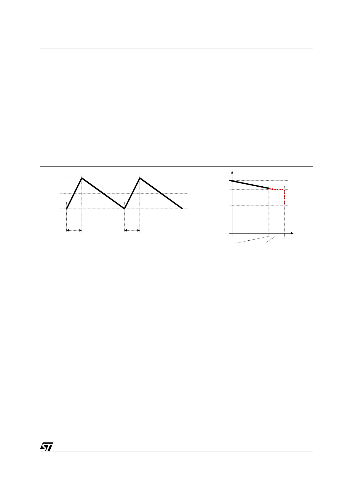
DYNAMIC VID TRANSITIO N
The device is able to manage On-The-Fly VID Code changes that allow Output Voltage modification during normal device operation. The device checks every clock cycle (synchronously with the PWM ramp) for VID code
modifications. Once the new code is stable for more than one clock cycle, the reference steps up or down in
25mV increments every c lock cycl e until the new VID code i s reached. Dur ing the tr ansiti on, VID code c hanges
are ignored; the device re-starts monitoring VID after the transiti on has finis hed. P GOOD, signal is masked during the transition and it is re-activated after the transition has finished while OVP / UVP are still active.
voltage reference (i.e. the set-point of the error amplifier). Internal pull-ups are
PROG
µ
A current generator up to 3.3V Typ); in this way, to program a logic "1" it is enough
Figure 2. Dynamic VID transition
VID
Reference
V
OUT
25mV steps transition
1 Clock Cycle Blanking Time
t
t
t
SOFT START AND INHIBIT
At start-up a ramp is generated increasing the loop reference from 0V to the final value programmed by VID in
2048 clock periods as shown in figure 3.
Before soft start, the l ower p ower MOS are turned ON after that VCCDR r eaches 2V (independentl y by V cc value) to discharge the output capacitor and to protect the load from high side mosfet failures. Once soft start begins, the reference is increased; also the upper MOS begins to switch and the output voltage starts to increase
with closed loop regulation. At the end of the digital soft start, the Power Good comparator is enabled and the
PGOOD signal is then driven high (See fig. 3). The Under Voltage comparator enabled when the reference voltage reaches 0.8V. The Soft-Start will not take place, if both VCC and VCCDR pins are not above their own turnon thresholds. During normal operation, if any under-voltage is detected on one of the two supplies the device
shuts down. Forcing the OSC/INH/FAULT pin to a voltage lower than 0.6V (Typ.), the device enters in INHIBIT
mode: all the power mosfets are turned off and protections are disabled.
Setting the I NH pin fr ee, causes the device to restart.
9/32
L6919C
Figure 3. Soft Start
VIN=V
CCDR
V
LGATEx
Turn ON threshold
2V
t
V
PGOOD
OUT
2048 Clock Cycles
Timing Diagram Acquisition:
t
t
t
CH1 = PGOOD; CH2 = V
Figure 4. Drivers peak current: High Side (left) and Low Side (right)
; CH4 = LGATEx
OUT
CH3 = HGATE1; CH4 = HGATE2 CH3 = LGATE1; CH4 = LGATE2
DRIVER SECTION
The integrated high-current drivers allow using different types of power MOS (also multiple MOS to reduce the
R
), maintaining fast switching transition.
dsON
The drivers for the high-side mosfets use BOOTx pins for supply and PHASEx pins for return. The drivers for
the low-side mosfets use VCCDRV pin for supply and PGND pin for return. A minimum voltage of 4.6V at VCCDRV pin is required to start operations of the device.
The controller embodies a sophisticated anti-shoot- through system to minimize low side body diode conduction
time maintaining good efficiency saving the use of Schottky diodes. The dead time is reduced to few nanoseconds assuring that high-side and low-side mosfets are never switched on simultaneously: when the high- side
mosfet turns off, the voltage on its source begins to fall; when the voltage reach es 2V, the low-side mosfet gate
drive is applied with 30ns delay. When the low-side mosfet turns off, the voltage at LGATEx pin is sensed. When
it drops below 1V, the high-side mosfet gate drive is applied with a delay of 30ns. If the current flowing in the
inductor is negativ e, the sourc e of high -side mos f et will nev er dr op. To all ow the tur ning on of the l ow-side mosfet even in this case, a watchdog controller is enabled: if the source of the high-side mosfet don't drop for more
than 240ns, the low side mosfet is switched on so allowing the negative current of the inductor to recirculate.
This mechanism allows the system to regulate even if the current is negative.
10/32

L6919C
The BOOTx and VCCDR pins are separated from IC's power supply (VCC pin) as well as signal ground (SGND
pin) and power ground (PGND pin) in order to maximize the switching noise immunity. The separated supply
for the diff erent drivers gives high flexibility in mosfet choice, allowing the use of logic- level mos fet. Several combination of supply can be chosen to optimize performance and efficiency of the application. Power conversion
is also flexible; 5V or 12V bus can be chosen freely.
The peak current is shown for both the upper and the lower driver of the two phases in figure 3. A 10nF capacitive load has been used. For the upper drivers, the source current is 1.9A while the sink current is 1.5A with
V
BOOT -VPHASE
VCCDR = 1 2V.
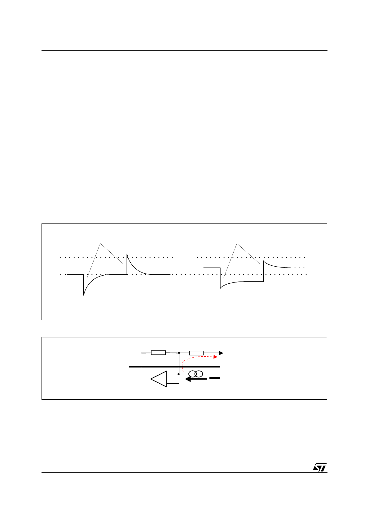
CURRENT READING AND OVER CURRENT
The current flowing trough each phase is read using the voltage drop across the low side mosfets R
across a sense resistor (R
by the external resistor Rg placed outsi de the chip between ISENx and PGNDSx pins toward the reading points.
The full differential current readi ng rejects noi se and allow s to plac e sensing el ement in different lo cations w ithout affecting the measurement's accuracy. The current reading circuitry reads the current during the time in
which the low-side mosfet is on (OFF Time). During this time, the reaction keeps the pin ISENx and PGNDSx
at the same voltage while during the time in which th e reading circ uitry is off, an internal clamp keeps these two
pins at the same voltage sinking from the ISENx pin the necessary current (Needed if low-side mosfet R
sense is implemented to avoid absolute maximum rating overcome on ISENx pin).
The proprietary current reading circuit allows a very precise and high bandwidth reading for both positive and
negative current. This circuit reproduces the current flowing through the sensing element using a high speed
Track & Hold Tran conductance amplifier. In particular, it reads the current during the second half of the OFF
time reducing noise injection into the device due to the mosfet turn-on (See fig. 5). Track time must be at least
200ns to make proper reading of the delivered current
= 12V; similar ly, for the low er driv ers, the source c urrent is 2.4A whi le the sink curr ent is 2A w ith
or
) and internally converted into a current. The Tran conductance ratio is issued
SENSE
dsON
dsON
Figure 5. Current Reading Timing (Left) and Circuit (Right)
I
LS1
LGATEX
I
LS2
Total current
information
ISENX
PGNDSX
Track & Hold
Rg
I
ISENx
Rg
50µµA
R
SENSE
PHASE
I
This circuit sources a constant 50µA current from the PGNDSx pin and keeps the pins ISENx and PGNDSx at
the same voltage. Referring to figure 4, the current that flows in the ISENx pin is then given by the following
equation:
R
⋅
+==
g
50µAI
INFOx
is the current car ried by each
PHASE
R
SENSEIPHASE
--------------------------------------- -------+
Where R
I
ISENx
is an external sense resi stor or the rds,on of the l ow side mosfet and Rg is the transconductance
SENSE
50µA
resistor used between ISE Nx and PGNDSx pins toward the readi ng points; I
phase and, in particular, the current measured in the middle of the oscillator period
The current information reproduced internally is represented by the second term of the previous equation as
11/32

L6919C
T
T
follow:
R
SENSEIPHASE
I
INFOx
----------------------------------------------=
Since the current is read in differential mode, also negative current information is kept; this allow the device to
check for dangerous returning current between the two phases assuring the complete equalization between the
phase's currents. From the current information of each phase, information about the total current delivered (I
=I
pared to I
INFO1
+I
) and the average current for each phase (I
INFO 2
to give the c orrection to the PW M output in order to equalize the current carr ied by the two phas es.
AVG
The transconductance resistor Rg can be designed in order to have current information of 25
full nominal load; the over current intervention threshold is set at 140% of the nominal (I
to the above relationship, the over current threshold (I
of the total delivered maximum current, results:
⋅
35µARg
I
OCPx
---------------------------=
R
SENSE
Since the device senses the output current across the low-side mosfets (or across a sense resistors in series
with them) the device limits the bottom of the inductor current triangular waveform: an over current is detected
when the current flowing into the sense element is greater than I
Introducing now the maximum ON time dependence with the delivered current (where T is the switching period
T=1/f
):
SW
T
ON,MAX
0.80 IFB5.73k
⋅()
⋅–
T
0.80
R
----------------------
⋅
R
g
=(I
AVG
) for each phase, which has to be placed at one half
OCPx
Rg
SENSE
Rg
+I
INFO 1
I
------------------------------------------ -=
OCPx
⋅⋅
I
OUT
INFO 2
⋅
OCPxRSENSE
35µA
(I
INFOx
5.73k
)/2 ) is taken. I
INFOX
µ
A per phase at
= 35µA). According
INFOx
> 35µA).
FB
FB
=
=
⋅
0.80 T I
⋅–==
T
⋅
0.40 T I
is then com-
FB
0µA
70µA
This linear dependence has a v alue at zero load of 0.80·T and at maximum current of 0.40·T typical and results
in two different behaviors of the device:
1. TON Limited Output Voltage.
This happens when the maximum ON time is reached before the current in each phase reaches I
OCPx
(I
INFOx
< 35µA).
Figure 6a show s the maximum output voltage that the device is able to regulate considering the T
imposed by the p revious re lations hip. If the desir ed o utput c haracter isti c cro sses the T
limited maximum output
ON
limitation
ON
voltage, t he ou tput r e sul ting vol t age will s tar t to drop after crossing. In this case, the device doesn't perfo r m co nstant current limitation but only limits the maximum ON time following the previous relationship. The output voltage follows the resulting characteristic (dotted in Figure 6b) until UVP is detected or anyway until I
= 70µA.
FB
Figure 6. TON Limited Operation
V
0.80·V
0.40·V
OUT
IN
IN
TON Limited Output
characteristic
I
OCP
(I
=2·I
=70µA)
FB
OCPx
I
OUT
V
0.80·V
0.40·V
OU
IN
IN
Resulting Output
characteristic
Desired Output
characteristic and
VP hrh
I
=2·I
OCP
OCPx
=70µA)
(I
FB
l
I
OU
a) Maximum output Voltage b) TON Limited Output Voltage
12/32
L6919C
(
2. Constant Current Operation
This happens when ON time limitation is reached after the current in each phase reach es I
The device enters in Quasi-Constant-Current operation: the low-side mosfets stays ON until the current read
becomes lower than I
a T
imposed by the control loop at the next available clock cycle and the device works in the usual way until
ON
OCPx
(I
< 35µA) skipping clock cycles. The high side mosfets can be turned ON with
INFO x
another OCP event is detected.
This means that the average curr ent delivered can sl ightly increase al so in Over Current condi tion since the cur -
rent ripple incr eases. In fact, the ON time incr eases due to the OFF time rise because of the c urrent has to r each
the I
bottom. The worst-case condition is when the ON time reaches its maximum value.
OCPx
When this happens, the device works in Constant Current and the output voltage decrease as the load increase.
Crossing the UVP threshold causes the device to latch (FAULT pin is driven high).
Figure 7 shows this working condition
Figure 7. Con s ta nt C urrent operat i on
Ipeak
I
MAX
Vout
Droop effect
OCPx
(I
INFO x
>35µA).
I
OCPx
TonMAX
a) Maximum current for each phase b) Output Characteristic
TonMAX
It can be observed that the peak current (Ipeak) is greater than the I
–
Where V
VINVout
-------------------------------------- -
Ipeak I
is the minimum output voltage (VID-30% as follow).
outMIN
OCPx
+
MIN
⋅
Ton
L
MAX
I
OCPx
OCPx
UVP
MAX,TOT
(IFB=50µA)
I
=2·I
OCP
IFB=70µA)
I
OCPx
but it can be determined as follow:
–
VINVout
-------------------------------------- -
+==
MIN
⋅⋅
L
0.40 T
Iout
The device works in Constant-Current, and the output voltage decreases as the load increase, until the output
voltage reaches the Under-Voltage threshold (V
). When this threshold is crossed, all mosfets are turned
outMIN
off, the FAULT pin is driven high and the device stops working. Cycle the power supply to restart operation. The
maximum average current during the Constant-Current behavior results:
=
I
MAX,TOT
2I
+
⋅
MAX
⋅
2I
OCPx
Ipeak I
------------------------------------- -+
OCPx
2
–
In this particular situation, the switching frequency results reduced. The ON time is the maximum allowed
(T
Over current is set anyw ay when I
to work with conv enient values for I
) while the OFF t i m e depends on the application:
onMAX
Ipeak I
------------------------------------- -
=
⋅
T
OFF
L
reaches 35µA (IFB = 70µA). The full load value i s only a co nvention
INFOx
. Since the OCP intervention t hreshol d is fixed, to modi fy the perc ent-
FB
V
–
OUT
OCPx
------------------------------------------=
f
T
ONma xTOFF
1
+
age with respect to the load val ue, it can be sim ply consider ed that, for example, to h ave on OCP thres hold
of 170%, this will correspond to I
I
= 20.6µA (IFB = 41.1µA).
INFOx
= 35µA (IFB = 70µA). The full load c urrent will then correspond to
INFOx
13/32
L6919C
(a) (b)
Integrated Droop Function
The device uses a droop function to satisfy the requirements of high perfor mance microprocessors, reducing
the size and the cost of the output capacitor.
This method "recovers" part of the drop due to the output capacitor ESR in the load transient, introducing a dependence of the output voltage on the load current
As shown in figure 8, the ESR drop is pr esent in any c ase, but using the droop func tion the total deviation of the
output voltage is minimized . In practice the dr oop function in troduces a static error (V
tional to the output c urrent. Si nce the devic e has an average c ur rent mode regulation, the information about the
total current delivered is used to implement the Droop Function. This current (equal to the sum of both I
is sourced from the FB pin. Connectin g a resistor between this pi n and V
, the total current information flows
OUT
only in this resi stor becaus e the compensation networ k between FB and COMP has al ways a capac itor in series
(See fig. 9). The voltage regulated is then equal to:
V
= VID - RFB · I
OUT
FB
Since IFB depends on the current information about the two phases, the output characterist ic vs . load current is
given by:
R
SENSE
----------------------
V
OUT
VID R
FB
⋅⋅–=
Rg
I
OUT
Figure 8. Output transient response without (a) and with (b) the droop function
in figure 8) propor-
DROOP
INFOx
)
ESR DROP ESR DROP
MAX
V
V
NOM
V
MIN
Figure 9. Active Droop Function Circuit
Z
F
COMP FB
V
PROG
R
FB
IFB
The feedback current is equal to 50µA at nominal full load ( IFB = I
threshold, so the maximum output voltage deviation is equal to:
To VOUT
INFO 1
+ I
) and 70µA at the OC intervention
INFO 2
V
DROOP
∆
V
FULL_POSITIVE_LOAD
= -RFB · 50µA
∆
V
OC_INTERVENTION
= -RFB · 70µA
Droop function is provided only for positive load; if negative load is applied, and then I
sunk from the FB pin. The device regulates at the voltage programmed by the VID.
14/32
< 0, no current is
INFOx

L6919C
OUTPUT VOLTAGE MONITOR AND PROTECTIONS
The output voltage is mo nitored by pi n V SEN. If i t is no t within ±12% (Typ.) of the program med value, the power
good output is forc ed low. Power good is an open drain output and it is enabl ed only after the soft start is fini shed
(2048 clock cycles after start-up).
The device provides over voltage protection; when the voltage sensed by the V
the controller permanently switches on both the low-side mosfets and switches off both the high-side mosfets
in order to protect the CPU. The OSC/INH/FAULT pin is driven high (5V) and power supply (Vcc) turn off and
on is required to restart operations . The over Vol tage percentage is s et by the r atio between the OVP thres hold
(set at 1.976V) and the reference programmed by VID.
pin reaches 1.976V (typ.),
SEN
[]
OVP %
---------------------------------------------------------------------- -
ReferenceVo ltage VID
1.976V
⋅=
()
100
Under voltage protection is also provided. If the output voltage drops below the 70% of the reference voltage for
more than one clock period the devic e turns off and the FAULT is driven high.
Both Over Voltage and Under Voltage are active also during soft start (Under Voltage after than V
OUT
reaches
0.8V). During soft-start the refer ence volta ge used to determine the U V thresho ld is the incr easing vol tage driven by the 2048 soft start digital counter.
REMOTE VOLTAGE SENSE
A remote sense buffer is integrated into the dev ice to allow output voltage remo te sense implementation without
any additional external components. In this way, the output voltage programmed is regulated between the remote buffer inputs compensating motherboard trace losses or connector losses if the device is used for a VRM
module. The very low offset amplifier senses the output vo ltage remotely through the pins FBR and FBG (FBR
is for the regulated voltage sense while FBG is for the ground sense) and reports this voltage internall y at VSEN
pin with unity gain eliminating the error s.
If remote sense i s not requir ed, the output v oltage is s ensed by the VSEN pin c onnecting it di rectly to the output
voltage. In this case the FBG and FBR pins must be connected anyway to the regulated voltage.
INPUT CAPACITOR
The input capacitor is designed considering mainly the input RMS current that depends on the duty cycle as
reported in figure 10. Considering the dual-phase topology, the input RMS current is highly reduced comparing
with a single phase operation.
Figure 10. Input RMS Current vs. Duty Cycle (D) and Driving Relationships
)
OUT
/I
RMS
0.50
0.25
Rms Current Normalized (I
Duty Cycle (V
Single Phase
Dual Phase
0.50 0.75 0.25
OUT/VIN
I
OUT
2
=
I
rms
)
I
OUT
2
<−⋅⋅
5.0DifD)2(12D
>−⋅⋅
0.5DifD)2(21)-(2D
15/32

L6919C
It can be observed that the input rms value is one half of the single-phase equivalent input current in the worst
case condition that happens for D = 0.25 and D = 0.75.
The power dissipated by the input capacitance is then equal to:
P
RMS
⋅=
ESR I
()
2
RMS
Input capacitor is designed in order to sustain the ripple relative to the maximum load duty cycle. To reach the
high RMS value needed by the CPU power supply application and also to minimize components cost, the input
capacitance is realized by more than one physical capacitor. The equivalent RMS current is simply the sum of
the single capacitor's RMS current.
Input bulk capacitor must be equally divided between high-side drain mosfets and placed as close as possible
to reduce switching noise above all during load transient. Cerami c capacitor can also intr oduce benefit s in high
frequency noise decoupling, noise generated by parasitic components along power path.
OUTPUT CAPACITOR
Since the microprocessors require a current variation beyond 50A doing load transients, with a slope in the
range of tenth A/
µ
s, the output capacitor is a basic component for the fast response of the power supply.
Dual ph ase to po logy reduc es th e am ount o f ou tput c apac itanc e ne eded b ecau se o f faste r lo ad tran sien t re spon se
(switching frequency is doubled at the load connections). Current ripple cancellation due to the 180° phase shift
between the tw o phase s also reduces requirements on the out put ESR to sustain a specified voltage ripple.
When a load transient is applied to the converter's output, for first few microseconds the current to the load is
supplied by the output capacitors. The controller recognizes immediately the load transient and increases the
duty cycle, but the current slope is limited by the inductor value.
The output voltage has a first drop due to the current variation inside the capacitor (neglecting the effect of the
ESL):
∆
V
OUT
= ∆I
OUT
· ESR
A minimum capacitor value is required to sustain the current during the load transient without discharge it. The
voltage drop due to the output capacitor discharge is given by the following equation:
2
∆
⋅
L
I
OUT
–⋅()⋅⋅
Where D
∆
V
OUT
is the maximum duty cycle value. The lower is the ESR, the lower is the output drop during load
MAX
-----------------------------------------------------------------------------------=
2C
OUTVINDMAXVOUT
transient and the lower is the output voltage static ripple.
INDUCTOR DESIGN
The inductance value is defined by a compromise between the transient response time, the efficiency, the cost
and the size. The inductor has to be calculated to sustain the output and the input voltage variation to maintain
the ripple current
∆
IL between 20% and 30% of the maximum output current. The inductance value can be cal-
culated with this relationship:
–
Where f
V
INVOUT
----------------------------- -
L
f
SWIL
is the switching frequency, VIN is the input voltage and V
SW
V
OUT
-------------- -
⋅=
∆⋅
V
IN
is the output voltage.
OUT
Increasing the value of the inductance reduces the ripple current but, at the same time, reduces the converter
response time to a load transient. The response time is the time required by the inductor to change its current
from initial to final value. Since the inductor has not finished its charging time, the output current is supplied by
the output capacitors. Minimizing the response time can minimize the output capacitance required.
The response time to a load transient is different for the application or the removal of the load: if during the ap-
16/32

L6919C
plication of the loa d the inductor is c harged by a voltage equal to the difference between the input and the output
voltage, during the removal it is discharged only by the output voltage. The following expressions give approximate response time for
∆
I load transient in case of enough fast compensation network response:
t
applicatio n
∆⋅
LI
------------------------------=
–
V
INVOUT
t
removal
∆⋅
LI
-------------- -=
V
OUT
The worst condition depends on the input voltage available and the output voltage selected. Anyway the worst
case is the response ti me after r emoval o f the load with the minimum output voltage programmed and the maximum input voltage available.
Figure 11. Inductor ripple current vs V
Inductor Ripple [A]
OUT
9
8
7
6
5
4
3
2
1
0
0.5 1.5 2.5 3.5
L=1.5µH, Vin=12V
L=3µH, Vin=5V
Output Voltage [V]
L=2µH,
Vin=12V
L=3µH,
Vin=12V
L=1.5µH,
Vin=5V
L=2µH,
Vin=5V
MAIN CONTROL LOOP
The control loop is composed by the Current Sharing control loop and the Average Current Mode control loop.
Each loop gives, with a proper gain, the correction to the PWM in order to minimize the error in its regulation:
the Current Sharing control loop equalize the currents in the inductors while the Average Current Mode control
loop fixes the output voltage e qual to the referen ce programmed by VID. Figur e 12 repor ts the bl ock di agram of
the main control loop.
Figure 12. Main Control Loop Diagram
+
+
D02IN1392
PWM1
1/5
1/5
PWM2
ERROR
AMPLIFIER
4/5
CURRENT
SHARING
DUTY CYCLE
CORRECTION
PROGRAMMED
+
-
Z
F(S)
REFERENCE
BY VID
FBCOMP
R
FB
I
INFO2
I
INFO1
L
1
L
2
C
O
R
O
17/32

L6919C
Current Sharing (CS) Control Loop
Active current sharing is implemented using the information from Tran conductance differential amplifier in an
average current mode control scheme. A current reference equal to the average of the read current (I
ternally built; the error between the read current and this reference is converted to a voltage with a proper gain
and it is used to adju st the duty c ycle whose d ominant val ue is set by the error am plifier at C OMP pin (See fi g. 13).
The current sharing control is a high bandwidth control loop allowing current sharing even during load transients.
The current sharing error is affected by the choice of external components; choose precise Rg resistor (±1% is
necessary) to sense the current. The current sharing error is internally dominated by the voltage offset of Tran
conductance differential amplifie r; consider ing a voltage offset equal to 2mV across the sense r esis tor, the current reading error is given by the following equation:
∆
Where
For R
∆
I
READ
SENSE
I
READ
------------------- -
I
MAX
is the difference between one phase current and the ideal current (I
= 4mΩ and I
= 40A the current sharing error is equal to 2.5%, neglecting errors due to Rg and
MAX
2mV
--------------------------------------- -=
R
SENSEIMAX
⋅
MAX
/2).
Rsense mismatches.
Figure 13. Current Shari n g C ontrol Loop
L
+
PWM1
1
AVG
) is in-
I
INFO2
I
INFO1
L
2
V
OUT
COMP
1/5
1/5
+
PWM2
CURRENT
SHARING
DUTY CYCLE
CORRECTION
D02IN1393
Average Current Mode (ACM) Control Loop
The average current mode control loop is reported in figure 14. The current information IFB sourced by the FB
pin flows into RFB implementing the dependence of the output voltage from the read current.
The ACM control loop gain results (obtained opening the loop after the COMP pin):
G
LOOP
()
s
PWM Z
--------------------------------------------------------------------------------------------------------------------=
()
Z
s
ZLs
P
s()R
F
()+()
DROOPZP
()
s
Z
F
-------------- -
As
1
()
1
----------- -+
()
As
()+()⋅⋅
s
⋅+⋅
R
FB
Where:
R
sense
– is the equivalent output resistance determined by the droop function;
R
DROOP
–Z
(s) is the impedance resulting by the parallel of the output capacitor (and its ESR) and the applied
P
------------------ -
R
⋅=
R
FB
g
load Ro;
(s) is the compensation network impedance;
–Z
F
(s) is the parallel of the two inductor impedance;
–Z
L
– A(s) is the error amplifier gain;
18/32

L6919C
C
F
Co
L
2
-- -
⋅
R
F
------------------- -=
∆
V
4
– · i s the ACM PWM transfer function where ∆V
PWM
-- -
5
and has a typical value of 2V
Removing the dependence from the Error Amplifier gain, so assuming this gain high enough, the control loop
gain results:
With further simplifications, it results:
()
LOOP
s
G
------------------ -
⋅=
∆
V
4
-- -
5
IN
OSC
------------------ -
⋅⋅⋅ ⋅–=
∆
V
V
G
LOOP
IN
OSC
()
s
()
Z
F
-------------- -
R
FB
4
-- -
⋅⋅ ⋅–=
5
s
+
Ro R
------------------------------------- -
Ro
V
IN
------------------ -
∆
V
OSC
DROOP
R
L
------ -+
2
is the oscillator ramp amplitude
OSC
()
s
Z
F
------------------------------------
s()ZLs
Z
P
Rs
------- -
()+
Rg
1sCoR
----------------------------------------------------------------------------------------------------------------------------------
2
s
Co
L
-- -
s
2
Z
P
---------------+
R
DROOP
L
---------------
⋅
2Ro
()
s
FB
+()⋅⋅+
//Ro ESR
Co ESR Co
R
------ -
⋅+⋅+
2
L
+⋅+⋅⋅
1
Considering now that in the application of interest it can be assumed that Ro>>R
R
<<Ro, it results:
DROOP
LOOP
()
G
()
Z
s
5
∆
V
OSC
V
4
IN
------------------ -
-- -
F
-------------- -
R
FB
s
----------------------------------------------------------------------------------------------------------------------------------⋅⋅⋅–=
2
s
1sCoR
L
---
Co
s
2
L
---------------
⋅
2Ro
DROOP
+()⋅⋅+
ESR
Co ESR Co
; ESR<<Ro and
L
R
L
------ -⋅+⋅+
+⋅+⋅⋅
1
2
The ACM control loop gai n is designed to obtain a high D C gain to m inimiz e static er ror and cr os s the 0dB ax es
with a constant -20dB/dec slope with the desired crossover frequency
ω
. Neglecting the effect of ZF(s), the
T
transfer function has one zero and two poles. Both the poles ar e fixed once the output filter is des igned and the
zero is fixed by ESR and the Droop resi stance. To obtain the de sir ed shape an R
ered for the Z
(s) implementation. A zero at
F
ω
=1/RFCF is then introduced together with an integrator. This in-
F
series network is co nsid-
F-CF
tegrator minimizes the static error while placing the zero in correspondence with the L-C resonance a simple 20dB/dec shape of the gain is assured (See Figure 14). In fact, considering the usual value for the output filter,
the LC resonance results to be at frequency lower than the abov e reported zero.Compensation netw ork can be
simply designed placing
RFBV
----------------------------------
R
F
ω
=
Z
∆⋅
V
and imposing the cross-over frequency
LC
IN
OSC
5
-- - ω
4
------------------------------------------------------- -⋅⋅ ⋅=
T
2R
L
DROOP
+()⋅
ESR
ω
as desired obtaining:
T
ω
Figure 14. ACM Control Loop Gain Block Diagram (left) and Bode Diagram (right)
dB
G
LOOP
K
ZF(s)
V
COMP
I
FB
F
Z
C
F
R
F
R
FB
REF
L/2
PWM
d•V
IN
Cout
ESR
V
OUT
ω
1
----------
R
FB
ω
dB
V
Rout
4
IN
---------------
-- -
K
⋅⋅
=
V
5
∆
osc
Z
LC
ω
T
ω
19/32

L6919C
LAYOUT GUIDE LINES
Since the device manages control functions and high -current driv ers, layout is one of the most imp ortan t things
to consider when designing such high current applications.
A good layout solution can generate a benefit in lowering power dissipation on the power paths, reducing radiation and a proper connection between signal and power ground can optimize the performance of the control
loops.
Integrated power drivers reduc e components count and interconnec tions between control fun ctions and drivers,
reducing the board space.
Here below are listed the main points to focus on when starting a new layout and r ules are suggested for a correct implementation.
■
Power Connections.
These are the c onnections wher e switching and continuous current fl ows from the input supp ly towards the load.
The first priority when placing components has to be reserved to this power section, minimizing the length of
each connection as much as possible.
To minimize noise and vol tage spikes (EMI and l osses) these interconnections must be a part of a power plane
and anyway realized by wide and thick copper traces. The critical components, i.e. the power transistors, must
be located as close as possible, together and to the controller. Considering that the "electrical" components reported in figure ar e com posed by more than one "phy sical " component, a ground plane or "star" grounding connection is suggested to minimize effects due to multiple connections.
Figure 15. Power connections and related connections layou t guidel ines (same for bo th phases)
VIN
HS
R
HGATEx
PHASEx
LGATEx
PGNDx
SGND
BOOTx
PHASEx
VCC
gate
L
C
LS
R
gate
D
C
IN
OUT
a. PCB power and ground planes areas
VIN
C
BOOTx
+VCC
HS
L
C
LS
D
C
IN
C
VCC
OUT
LOAD
LOAD
20/32
b. PCB small signal components placement

L6919C
Fig. 15a shows the details of the power conn ections involved a nd the current lo ops. The input capaci tance (CIN),
or at least a portion of the total capacitance needed, has to be placed close to the power section in order to
eliminate the stray inductance generated by the copper traces. Low ESR and ESL capacitors are required.
■
Power Connec t i ons Related.
Fig.15b shows some small signal components placement, and how and where to mix signal and power ground
planes. The distance from drivers and mosfet gates should be reduced as much as possible. Propagation delay
times as well as for the voltage spikes generated by the distributed inductance along the copper traces are so
minimized.
In fact, the further the mosfet is from the device, the longer is the interconnecting gate trace and as a consequence, the higher are the voltage spikes corresponding to the gate PWM rising and falling signals. Even if
these spikes are clamped by inherent internal diodes, propagation delays, noise and potential causes of instabilities are introduced jeopardizing good system behavior. One important consequence is that the switching
losses for the high side mosfet are significantly increased.
For this reason, it is suggested to have the device oriented w ith the driver side towards the mosfets and the
GATEx and PHASEx traces walking together toward the high side mosfet in or der to minimi ze distanc e (see fig
16). In addition, since the PHASEx pin is the return path for the high side driver, this pin must be connected
directly to the High Side mosfet Source pin to have a proper driving for this mosfet. For the LS mosfets, the return path is the PGND pin: it can be connected directly to the power ground plane (if implemented) or in the
same way to the LS mosfets Source pin. G ATEx and PHASEx connections (and also PGND when no power
ground plane is implemented) must also be designed to handle current peaks in excess of 2A (30 mils wide is
suggested).
Gate resistors of few ohms help in reducing the power dissipated by the IC without compromising the system
efficiency.
Figure 16. Device orientation (left) and sense nets routing (right)
To LS mosfet
Towards HS mosfet
(30 mils wide)
Towards LS mosfet
(30 mils wide)
Towards HS mosfet
(30 mils wide)
(or sense resistor)
To LS mosfet
(or sense resistor)
Toregulatedoutput
The placement of other components is also important:
– Th e bootstrap c apacitor must be placed as clos e as possible to the BOOTx and PHASEx pins to mini-
mize the loop that is created.
– Decoupling capacitor from Vcc and SGND placed as close as possible to the involved pins.
– Decoupling capacitor from VCCDR and PGND placed as close as possi ble to those pins. T his capacitor
sustains the peak currents requested by the low-side mosfet drivers.
– Refer to SGND all the sensible components such as frequency set-up resistor (when present) and also
the optional resistor from FB to GND used to give the positive droop effect.
– Connect SGND to PGND on the load side (output capacitor) to avoid undesirable load regulation effect
and to ensure the right precision to the regulation when the remote sense buffer is not used.
21/32

L6919C
– An additional 100nF ceramic capacitor is suggested to place near HS mosfet drain. This helps in reduc-
ing noise.
– PHASE pin spikes. Since the HS mosfet switches in hard mode, heavy voltage spikes can be observed
on the PHASE pins. If these voltage spikes overcome the max breakdown voltage of the pin, the device
can absorb energy and it can cause damages. The voltage spikes must be limited by proper layout, the
use of gate resistors, Schottky diodes in parallel to the low side mosfets and/or snubber network on the
low side mosfets, to a value lower than 26V, for 20nSec, at FSW of 600kHz max.
■
Current S ens e Connectio ns .
Remote Buffer:
pins to the load in order to compensate losses along the output power traces and also to avoid the pick-up of
any common mode noise. Connec ting these pi ns i n points far fr om the l oad, w ill cause a non -optimum l oad r egulation, increasing output tolerance.
Current Reading:
order to limit the noise injection into the device. The PCB traces connecting these resistors to the reading point
must be routed as parallel traces in order to avoid the pick-up of any common mode noise. It's also important
to avoid any offset in the measurement and to get a better precision, to connect the traces as cl ose as possi ble
to the sensing elements, dedicated current sense resistor or low side mosfet R
Moreover, when using the low side mosfet R
nected to the PHAS Ex pin. DO N OT CONNEC T THE PIN S TOGETHER AND TH EN TO THE H S SOURC E!
The device won't work properly because of the noise generated by the return of the high side driver. In this case
route two separate nets: connect the PHASEx pin to the HS Source (route together with HGATEx) with a wide
net (30 mils) and the ISENx pin to the LS Drain (route together with PGNDSx). Moreover, the PGNDSx pin is
always connected, through the Rg resistor, to the PGND: DO NOT CONNECT DIRECTLY TO THE PGND! In
this case the device won't work properly. Route anyway to the LS mosfet source (together with ISENx net).
Right and wrong connections are reported in Figure 17.
Symmetrical layout is also suggested to avoid any unbalance between the two phases of the converter.
The input connections for this components must be routed as parallel nets from the FBG/FBR
The Rg resistor has to be placed as close as possible to the ISENx and PGNDSx pins in
.
dsON
as current sense element, the ISENx pin is practically con-
dsON
Figure 17. PCB layout connections for sense nets
NOT CORRECT
VIA to GND plane
ToPHASE
connection
Wrong (left) and correct (right) connections for the current reading sensing nets.
CORRECT
To LS Drain
and Source
To HS Gate
and Source
22/32

L6919C
Demo Board Description
The L6919C demo board shows the operation of the device in a dual phase application. This evaluation board
allows output voltage adjustability (0.800V - 1.550V) through the switches S0-S4 and high output current capability.
The board has been laid out with the possi bility to use up to two D
to give maximum flexibility in the mosfet choice.
The four layers demo boar d's copper thickness is of 70
µ
m in order to minimize conduction losses considering
the high current that the circuit is able to deliver.
Demo board schematic circuit is reported in Figure 18.
Figure 18. Demo Board Schematic
Vin
GNDin
Vcc
GNDcc
JP6
S4
S3
S2
S1
S0
To pin
VCC
DZ1
JP1
C5
L1
D4
Q2
C4
Q1
D1
Q1a
R21
JP2
R16
R2
VCCDR
C8
R15
R18
R13
R6
R5
2
BOOT1
5
UGATE1
4
PHASE1
3
LGATE1
1
ISEN1
13
PGNDS1
VID4
VID3
VID2
VID1
VID0
OSC / INH
SGND
14
L6919C
22
21
20
19
18
17
7
11
FBR
U1
VCC
6
BOOT2
24
UGATE2
25
PHASE2
26
LGATE2
27
ISEN2
16
PGNDS2
15
PGND
28
PGOOD
23
VSEN
10
FB
9
COMP
8
12
FBG
2
PACK mosfets for the low side sw itch in order
C11..C13
R11
C7
R14
R17
R12
R3
D3
Q4 C3
Q3
Q3a
C6
L2
D2
R4
R10
R7
C24
R8
C2
C1
JP3
R9
C9,C10
R19
C14,
C23
R1
R20
JP4
VoutCORE
GNDCORE
PGOOD
JP5
FBG
FBR
Several jumpers allow setting different configurations for the device: JP3, JP4 and JP5 allow configuring the
remote buffer as desired. Simply shorting JP4 and JP5 the remote buffer is enabled and it senses the output
voltage on-board; to implement a real remote sense, leave these jumpers open and connect the FBG and FBR
connectors on the demo board to the remote load. To avoid usi ng the remote buffer, simpl y short all the j umpers
JP3, JP4 and JP5. Local sense through the R7 is used for the regulation.
The input can be configured in different ways using the jumpers JP1, JP2 and JP6; these jumpers control also
the mosfet driver supply v oltage. Anyway, power c onversion starts fr om V
and the device is suppl ied from V
IN
CC
(See Figure 19).
Figure 19. Power supply conf i gu ra ti on
Vin
GNDin
Vcc
GNDcc
To Vcc pin
JP6
DZ1
JP1
JP2
To HS Drains (Pow er Input)
To BOOTx (HS Driver Supply)
To VCCDR pi n (LS Driver Supply)
23/32

L6919C
V
Two main configurations can be distinguished: Single Supply (VCC=VIN=12V) and Double Supply (VCC=12V
VIN=5V or different).
– Single Supply: In this case JP6 has to be completely shorted. The device is supplied with the same rail
that is used for the conversion. With an additional zener diode DZ1 a lo wer voltage can be derived to
supply the mosfets driver if Logic level mosf et are us ed. In this c ase J P1 must be left op en so th at the
HS driver is supplied with V
the right to use V
and JP2 can be freely shorted in one of the two positions.
– Doubl e Supply: In this case VCC s upply directly the controller (12V) while V
for the power conversion. This last one can start indifferently from the 5V bus (Typ.) or from other buses
allowing maximum flexibility in the power conversion. Supply for the mosfet driver can be programmed
through the jumpers JP1, JP2 and JP6 as previously illustrated. JP6 selects now V
on the requirements.
Some examples are reported in the following Figures 20 and 21.
Figure 20. Jumpers configuration: Double Supply
IN-VDZ1
IN-VDZ1
to supply the LS driver through VCCDR pin. Otherwise, JP1 must be shorted
through BOOTx and JP2 must be shorted to the left to use VIN or to
supplies the HS drains
IN
or VIN depending
CC
Vcc = 12V
Vcc = 12V
Figure 21. Jumpers configuration: Single Supply
Vcc = Open
Vin = 5V
GNDin
GNDcc
Vin = 5V
GNDin
GNDcc
Vin = 12V
GNDin
JP6
(a) V
= 12V; V
CC
DZ1
JP6
(b) V
CC
= V
DZ1
BOOTx
JP6
DZ1 6.8V
Vcc = 12V
HS Drains = 5V
JP2
JP1
= VCCDR = VIN = 5V
BOOTx
JP2
JP1
= VCCDR = 12V; VIN = 5V
JP1
HS Supply = 5V
VCCDR (LS Supply) = 5V
Vcc = 12V
HS Drains = 5V
HS Supply = 12V
VCCDR (LS Supply) = 12
Vcc = 12V
HS Drains = 12V
HS Supply = 5.2V
JP2
VCCDR (LS Supply) = 12V
24/32
GNDcc
(a) VCC = VIN = VCCDR = 12V; V
Vcc = Open
Vin = 12V
GNDin
GNDcc
JP6
DZ1
JP1
JP2
(b) V
= VIN = V
CC
= VCCDR = 12V
BOOTx
= 5.2V
BOOTx
Vcc = 12V
HS Drains = 12V
HS Supply = 12V
VCCDR (LS Supply) = 12V

PCB AND COMPONENT LAYOUT
Figure 22. PCB and Components Layouts (Dimensions: 10.8mm x 8.2mm)
L6919C
Component Side
Internal PGND Plane
Internal SGND Plane
Solder Side
25/32

L6919C
CPU Power Supply: 5 to 12VIN; 1.2V
OUT
; 45A
DC
Considering the high slope for the load transient, a high switching frequency has to be used. In addition to fast
reaction, this helps in reducing output and input capacitor. Inductance value is also reduced.
A switching frequency of 200kH z for each phase is then considered allowing large bandwidth for the compensation network. Considering the high output current, power conversion will start from the 12V bus.
– Current Reading Network and Over Current:
Since the maximum output current is I
= 45A, the over current threshold has been set to 45A (22.5A
MAX
x 2)in the worst case (max mosfet temperature). Since the device limits the valley of the triangular ripple
across the inductors, the current ripple must be considered too. Considering the inductor core satura-
tion, a current ripple of 10A has t o be considered s o that the OCP threshold in wors t case becomes
OCPx=17A (22.5A-5A). Considering to sense the output current across the low-side mosfet RdsON,
SUB85N03L-04P has 4.3mΩ max at 25°C that becomes 5.6mΩ at 100ºC considering the temperature
variation; the resulting transconductance resistor Rg has to be:
R
dsON
----------------- -
OCPx
⋅
µ
35
===
Rg I
17
5.6m
-------------
⋅
35
2.7kΩ (R3 to R6)
µ
– Droop func tion Design:
Considering a voltage drop of 70mV at full load, the feedback resistor R
70mV
----------------
==
R
FB
70µA
1kΩ (R7)
has to be:
FB
– Induc to r design:
Transient response performance ne eds a comp romi se in the induct or ch oice value: t he bigg est the in-
ductor, the highest the efficient but the worse the transient response and vice versa.
Considering then an inductor value of 0.8µH, the current ripple becomes:
–
Vin Vout
== =
∆
---------------------------- -
I
L
d
-----------⋅
Fsw
–
12 1.2
-------------------- -
µ
0.8
1.2
------- -
12
1
------------ -⋅⋅
200k
6.5A (L1, L2)
– Output Capacitor:
Five Rubycon MBZ (2200µF / 6.3V / 12mΩ max ESR) has been used implementing a resulting ESR of
2.4mΩ resulting in an ESR voltage drop of 45A · 2.4mΩ = 108mV after a 45A load transient.
– Com pensat ion Network :
A voltage loop bandwidth of 20kHz is considered to let the device fast react after load transient.
The R
R
== =
F
network results:
F CF
R
∆⋅
IN
5
-- -
ω
⋅⋅ ⋅
T
4
FBVOS
------------------------------
V
-------------------------------------------------------
2R
L
()⋅
DROOP
== =
C
F
ESR
+
⋅
Co
------------------- -
R
F
1K 2⋅
---------------
12
L
-- -
62200
2
---------------------------------------- -
2k
5
-- -
4
20 K 2Π
µ
1
------ -
µ
⋅⋅
2
---------------------------------------------------------------
⋅⋅⋅⋅ 2.0kΩ
2
33nF
0.8 µ
5.6m
-------------
1.2k 2.4m
⋅
⋅
2.7
+
(R8)
(C2)
Further adjustments can be done on the work bench to fit the requirements and to compensate layout parasitic
components.
26/32

Part List
R1 10k SMD 0805
R2, R20,R21 Not Mounted SMD 0805
R3, R4, R5, R6 2.7k 1% SMD 0805
R7 1k 1% SMD 0805
R8 1.8k SMD 0805
R9 47k 1% SMD 0805
R10 510 SMD 0805
R11 82 SMD 0805
R12 to R19 0 SMD 0805
C1 Not Mounted SMD 0805
C2 22n SMD 0805
C3, C4 100n SMD 0805
C5, C6, C7, C8 1
C9, C10 10
C11 to C13 1800
C14 to C18 2200
µ
µ
or 22µ / 16V TDK Multilayer Ceramic SMD 1206
µ
/ 16V Rubycon MBZ Radial 10x23
µ
/ 6.3V Rubycon MBZ Radial 10x20
Ceramic SMD 1206
C24 100n SMD 0805
L6919C
L1, L2 0.8
µ
77121 - 4Turns
U1 L6919C STMicroelectronics SO28
2
Q1, Q3 SUB85N03-04P Vishay D
Q2, Q4 SUB70N03-09BP Vishay D
PACK
2
PACK
D1, D2 STPS340U STMicroelectronics SMB
D3, D4 1N4148 STMicroelectronics SOT23
S0,S4 Short
S1,S2,S3 Open
STATIC PERFORMANCES
Figure 23 shows the demo board measured efficiency versus load current in steady state conditi ons without airflow at ambient temperature.
Figure 23. System Efficiency
90
85
80
75
70
65
Efficiency [%]
60
55
50
0 5 10 15 20 25 30 35 40 45
Output Current [A]
27/32

L6919C
Figure 24 shows the mosfets temper ature versus output current in steady state condition without any air-flow
or heat sink. It can be observed that the mosfets are under 100ºC in any conditions. Load regulation is also reported from 10A to 45A.
Figure 24. Mosfet Temperature and Load Regulation
100
90
C]
o
80
70
60
50
40
MOS Temperature [
30
20
0 5 10 15 20 25 30 35 40 45
High-side MOS Q2
High-side MOS Q4
Low -side MOS Q1
Low -side MOS Q3
Output Current [A]
1.250
1.240
1.230
1.220
1.210
Vout [V]
1.200
1.190
1.180
1.170
0 5 10 15 20 25 30 35 40 45
Output Current [A]
DYNAMIC PERFORMANCES
Figure 25 shows the system response to a load trans ient from 3A to 45A . The output voltag e is c ontained i n the
±50mV range. Additional output capacitors can help in reducing the initial voltage spi ke mainly due to the ESR.
Figure 25. 3A to 45A Load Transient Response
Figure 26 sh ows t he s ystem r espon se to a VID transient f rom 1.2 00V t o 0.800 V and vice v ersa at min imum load (3 A).
Figure 26. Dynamic VID Response
28/32

L6919C
DEMO BOARD ENHANCEMENTS: 1.200V / 52A CPU Power Supply
Considering the same application schematic, minor changes can be done to achieve the 52A thermal output
current required by AMD Hammer processor core. Part list has been modified as follow:
Part List
R1, R2, R20,R21 Not Mounted SMD 0805
R3, R4, R5, R6 1.5k 1% SMD 0805
R7 1k 1% SMD 0805
R8 1.8k SMD 0805
R9 47k 1% SMD 0805
R10 510 SMD 0805
R11 82 SMD 0805
R12 to R19 0 SMD 0805
C1 Not Mounted SMD 0805
C2 10n SMD 0805
C3, C4 100n SMD 0805
C5, C6, C7, C8 1
C9, C10 10
C11 to C13 1800
C14 to C18 2200
C24 100n SMD 0805
µ
µ
or 22µ / 16V TDK Multilayer Ceramic SMD 1206
µ
/ 16V Rubycon MBZ Radial 10x23
µ
/ 6.3V Rubycon MBZ Radial 10x20
Ceramic SMD 1206
L1, L2 0.8
µ
77121 - 4Turns
U1 L6919C STMicroelectronics SO28
Q1, Q1a, Q3, Q3a SUB85N03-04P Vishay-Siliconix D
Q2, Q4 SUB70N03-09BP Vishay-Siliconix D
2
PACK
2
PACK
D1, D2 STPS340U STMicroelectronics SMB
D3, D4 1N4148 STMicroelectronics SOT23
S0,S4 Short
S1,S2,S3 Open
STATIC PERFORMANCES
Figure 27 shows the demo board measured efficiency versus load current in steady state conditi ons without airflow at ambient temperature.
Figure 27. System Efficiency
90
85
80
75
70
65
60
Efficiency [%]
55
50
45
40
0 5 10 15 20 25 30 35 40 45 50 55 60
Output Curre nt [ A]
29/32

L6919C
Figure 28 shows the mosfets temper ature versus output current in steady state condition without any air-flow
or heat sink. It can be observed that the mosfets are under 105°C in any conditions. Load regulation is also reported from 10A to 55A.
Figure 28. Mosfet Temperature and Load Regulation.
115
105
C]
o
95
85
75
65
55
45
MOS Temperature [
35
25
High- side MOS Q2
High- side MOS Q4
Low-side MO S Q1
Low-side MO S Q3
0 5 10 15 20 25 30 35 40 45 50 55 60
Output Current [A]
1.235
1.225
1.215
1.205
1.195
Vout [V]
1.185
1.175
1.165
1.155
0 5 10 15 20 25 30 35 40 45 50 55 60
Output Current [A]
Figure 29 shows the system response to a load trans ient from 3A to 45A . The output voltag e is c ontained i n the
±50mV range. Additional output capacitors can help in reducing the initial voltage spi ke mainly due to the ESR.
Figure 29. 3A to 45A Load Transient Response
Figure 30 shows t he system respo nse to a VI D trans ient f rom 1.200V t o 0 .800V and vice ver sa at mi nim um load ( 3A) .
Figure 30. Dynamic VID Response
30/32
L6919C
DIM.
MIN. TYP. MAX. MIN. TYP. MAX.
A 2.65 0.104
a1 0.1 0.3 0.004 0.012
b 0.35 0.49 0.014 0.019
b1 0.23 0.32 0.009 0.013
C 0.5 0.020
c1 45° (typ.)
D 17.7 18.1 0.697 0.713
E 10 10.65 0.394 0.419
e 1.27 0.050
e3 16.51 0.65
F 7.4 7.6 0.291 0.299
L 0.4 1.27 0.016 0.050
S8° (max.)
mm inch
OUTLINE AND
MECHANICAL DATA
SO28
31/32

L6919C
Information furnished is believed to be accurate and reliable. However, STMicroelectronics assumes no responsibility for the consequences
of use of such information nor for any infringement of patents or other rights of third parties which may result from its use. No license is granted
by implic ation or otherwise under any patent or p at ent rights of STMicroelectronics. Spec i fications mentioned i n this publication are subject
to change without notice. This publication supersedes and replaces all information previously supplied. STMicroelectronics products are not
authorized for use as cri t i cal compone nts in life support device s or systems without express written approval of STMicroel ectronics.
The ST logo is a registered trademark of STMicroelectronics
2002 STMi croelectronics - All Ri ghts Rese rved
Australia - Brazil - Canada - Ch i na - F i nl and - France - Germany - Hong Kong - In di a - Israel - Ital y - Japan -Ma l aysia - Malta - Morocco -
Singap ore - Spain - Sweden - Swit zerland - Uni ted Kingdom - United States.
STMicroelectronics GROUP OF COMPANIES
http://www.s t. com
32/32
 Loading...