


5 BIT PROGRAMMABLE DUAL-PHASE CONTROLLER
WITH DYNAMIC VID MANAGEMENT
■
2 PHASE OPERATION WITH
SYNCRHONOUS RECTIFIER CONTROL
■
ULTRA FAST LOAD TRANSIENT RESPONSE
■
INTEGRATED HIGH CURRENT GATE
DRIVERS: UP TO 2A GATE CURRENT
■
TTL-COMP A T I BLE 5 BIT P ROGR AMMABLE
OUTPUT FROM 0.800V TO 1.550V WITH
25mV STEPS
■
DYNAMIC VID MANAGEMENT
■
0.6% OUTPUT VOLTAGE ACCURACY
■
10% ACTIVE CURRENT SHARIN G ACCURACY
■
DIGITAL 2048 STEP SOFT-START
■
OVERVOLTAGE PROTEC T I O N
■
OVERCURRENT PROTECTION REALIZED
USING THE LOWER MOSFET'S R
SENSE RESISTOR
■
OSCILLATOR EXTERNALLY ADJUST ABLE
AND INTERNALLY FIXED AT 200kHz
■
POWER GOOD OUTPUT AND INHIBIT
FUNCTI ON
■
REMOTE SENSE BUFFER
■
PACKAGE: SO-28
APPLICATION S
■
POWER SUPPLY FOR SERVERS AND
WORKSTATIONS
■
POWER SUPPLY FOR HIGH CURRENT
MICROPROCESSORS
■
DISTRIBUTED PO WE R SUPP LY
dsON
OR A
L6919C
SO-28
ORDERING NUMBERS:L6919CD
L6919CDTR
DESCRIPTION
The device is a power supply controller specifically designed to provide a high performance DC/DC conversion for high current microprocessors. The device
implements a dual-phase step-down controller with a
180° phase-shift between each phase. A precise 5-bit
digital to analog converter (DAC) allows adjusting the
output volt age from 0.800V to 1.550V with 25mV binary
steps managi ng O n-The-Fly VID code changes.
The high precision internal r eference ass ures the selected output voltage to be within ±0.6%. The high
peak current gate drive affor ds to hav e fast s witching
to the external power mos providing low switching
losses.
The device assures a fast protection against load
over current and load over/under vol t age. An internal
crowbar is provided turning on the low side mosfet if
an over-voltage is detected. In case of over-current,
the system works in Constant Current mode.
BLOCK DIAGRAM
PGOOD
PGOOD
December 2002
VID4
VID4
VID3
VID3
VID2
VID2
VID1
VID1
VID0
VID0
FBG
FBG
FBR
FBR
DIGITAL
DIGITAL
SOF T- S TAR T
SOF T- S TAR T
DAC
DAC
32k
32k
32k
32k
32k
32k
32k
32k
REMOTE
REMOTE
BUFFE R
BUFFE R
OSC / INH SGND VCCDR
OSC / INH SGND VCCDR
PWM1
TO TA L
TO TA L
CURRENT
CURRENT
CURRENT
CURRENT
PWM1
AVG
AVG
PWM2
PWM2
LOGIC PWM
LOGIC PWM
LOGIC PWM
ADAPTIVE ANTI
ADAPTIVE ANTI
CH1
CH1
OCP
OCP
CURRENT
CURRENT
CORRECTION
CORRECTION
CH2
CH2
OCP
OCP
CURRENT
CURRENT
CORRECTION
CORRECTION
ADAPTIVE ANTI
CRO SS C OND U CT ION
CRO SS C OND U CT ION
CRO SS C OND U CT ION
CURRENT
CURREN T
CURREN T
READING
READING
READING
CURREN T
CURREN T
CURREN T
READING
READING
READING
LOGIC PWM
LOGIC PWM
LOGIC PWM
ADAPTIVE ANTI
ADAPTIVE ANTI
ADAPTIVE ANTI
CROSS CONDUCTION
CROSS CONDUCTION
CROSS CONDUCTION
Vcc
Vcc
VccCOM PFBVSEN
VccCOM PFBVSEN
I
I
FB
FB
2 PH AS E
2 PH AS E
LOGIC AND
LOGIC AND
CH1 OCP
CH1 OCP
OSCILLATOR
OSCILLATOR
PROTECTIONS
PROTECTIONS
CH2 OCP
CH2 OCP
VCC
VCC
VCCDR
VCCDR
ERROR
ERROR
A MPLIF IER
A MPLIF IER
BOO T 1
BOO T 1
HS
HS
LS
LS
LS
LS
HS
HS
U
U
GA T E 1
GA T E 1
PHASE1
PHASE1
LGATE1
LGATE1
ISEN1
ISEN1
PGNDS1
PGNDS1
PGND
PGND
PGNDS2
PGNDS2
ISEN2
ISEN2
LGATE2
LGATE2
PHASE2
PHASE2
UGATE2
UGATE2
BOO T 2
BOO T 2
1/32
L6919C
ABSOLUTE MAXIMUM RATINGS
Symbol Parameter Value Unit
Vcc, V
CCDR
V
BOOT-VPHASE
V
UGATE1-VPHASE1
V
UGATE2-VPHASE2
V
phase
THERMAL DATA
Symbol Parameter Value Unit
to PGND 15 V
Boot Voltage 15 V
15 V
LGATE1, PHASE1, LGATE2, PHASE2 to PGND -0.3 to Vcc+0.3 V
VID0 to VID4 -0.3 to 5 V
All other pins to PGND -0.3 to 7 V
Sustainable Peak Voltage t < 20ns @ 600kHz 26 V
R
th j-amb
T
T
storage
P
Thermal Resistance Junction to Ambient 60 °C/W
Maximum junction temperature 150 °C
max
Storage temperature range -40 to 150 °C
T
Junction Temperature Range 0 to 125 °C
j
Max power dissipation at T
MAX
PIN CONNECTION
LGATE1
VCCDR
PHASE1
UGATE1
BOOT1
VCC
SGND
COMP
FB
VSEN
FBR
FBG
ISEN1
PGNDS1
= 25°C 2 W
amb
1
2
3
4
5
6
7
8
9
10
11
12
13
14
L6919C
28
27
26
25
24
23
22
21
20
19
18
17
16
15
PGND
LGATE2
PHASE2
UGATE2
BOOT2
PGOOD
VID4
VID3
VID2
VID1
VID0
OSC / INH / FAULT
ISEN2
PGNDS2
2/32

L6919C
ELECTRICAL CHARACTERISTICS
= 12V
V
CC
Symbol Parameter Test Condition Min Typ Max Unit
Vcc SUPPLY CURRENT
±10%
, TJ = 0 to 70°C unless otherwise specified
I
CC
I
CCDR
I
BOOTx
Vcc supply current HGATEx and LGATEx open
V
V
supply current LGATEx open; V
CCDR
CCDR=VBOOT
=12V
=12V 2 3 4 mA
CCDR
Boot supply current HGATEx open; PHASEx to PGND
V
CC=VBOOT
=12V
7.5 10 12.5 mA
0.5 1 1.5 mA
POWER-ON
Turn-On V
Turn-Off V
Turn-On V
Threshold
Turn-Off V
Threshold
threshold VCC Rising; V
CC
threshold VCC Falling; V
CC
V
CCDR
CCDR
Rising
VCC=12V
V
CCDR
CCDR
Falling
VCC=12V
=5V 8 9.2 10.4 V
CCDR
=5V 6.5 7.5 8.5 V
CCDR
4.2 4.4 4.6 V
4.0 4.2 4.4 V
OSCILLATOR/INHIBIT/FAULT
f
OSC
f
OSC,Rosc
INH Inhibit threshold I
d
Initial Accuracy OSC = OPEN
OSC = OPEN; Tj=0°C to 125°C
185
180
200 215
Total Accuracy RT to GND=74kΩ 360 400 440 kHz
=5mA 0.5 V
SINK
Maximum duty cycle OSC = OPEN; IFB = 0 75 80 %
MAX
OSC = OPEN; I
= 60µA3846 %
FB
220
∆Vosc Ramp Amplitude 1.8 2 2.2 V
kHz
kHz
FAULT Voltage at pin OSC OVP or UVP Active 4.75 5.0 5.25 V
REFERENCE AND DAC
-0.6 - 0.6 %
I
DAC
Output Voltage
Accuracy
VID0, VID1, VID2, VID3, VID4
see Table1;
FBR = V
; FBG = GND
OUT
VID pull-up Current VIDx = GND 4 5 6 µA
VID pull-up Voltage VIDx = OPEN 3.2 - 3.5 V
ERROR AMPLIFIER
DC Gain 80 dB
SR Slew-Rate COMP=10pF 15 V/µs
DIFFERENTIAL AMPLIFIER (REMOTE BUFFER)
DC Gain 1 V/V
CMRR Common Mode Rejection Ratio 40 dB
SR Slew Rate VSEN=10pF 15 V/µs
3/32

L6919C
ELECTRICAL CHARACTERISTICS
V
= 12V
CC
±10%
, TJ = 0 to 70°C unless otherwise specified
(continued)
Symbol Parameter Test Condition Min Typ Max Unit
DIFFERENTIAL CURRENT SENSING
,
I
ISEN1
I
ISEN2
I
PGNDSx
I
ISEN1
I
ISEN2
I
FB
Bias Current I
Bias Current 45 50 55 µA
,
Bias Current at
Over Current Threshold
Active Droop Current I
= 0 45 50 55 µA
LOAD
80 85 90 µA
LOAD
I
LOAD
≤ 0%
= 100%
47.5
0
50
1
52.5
GATE DRIVERS
t
RISE
HGATE
I
HGATEx
High Side
Rise Time
High Side
V
BOOTx-VPHASEx
C
V
to PHASEx=3.3nF
HGATEx
BOOTx-VPHASEx
=10V;
15 30 ns
=10V 2 A
Source Current
R
HGATEx
High Side
V
BOOTx-VPHASEx
=12V; 1.5 2 2.5 Ω
Sink Resistance
t
RISE
LGATE
I
LGATEx
Low Side
Rise Time
Low Side
V
=10V;
CCDR
C
V
to PGNDx=5.6nF
LGATEx
=10V 1.8 A
CCDR
30 55 ns
Source Current
µA
µA
R
LGATEx
Low Side
Sink Resistance
PROTECTIONS
PGOOD Upper Threshold
(V
/DAC Output)
SEN
PGOOD Lower Threshold
/DAC Output)
(V
SEN
OVP Over Voltage Threshold
)
(V
SEN
UVP Under Voltage Trip
/DAC Output)
(V
SEN
V
PGOOD
PGOOD Voltage Low I
V
=12V 0.7 1.1 1.5 Ω
CCDR
V
Rising 108 112 116 %
SEN
V
Falling 84 88 92 %
SEN
V
Rising 1.915 2.05 V
SEN
V
Falling 65 70 75 %
SEN
= -4mA 0.3 0.4 0.5 V
PGOOD
4/32
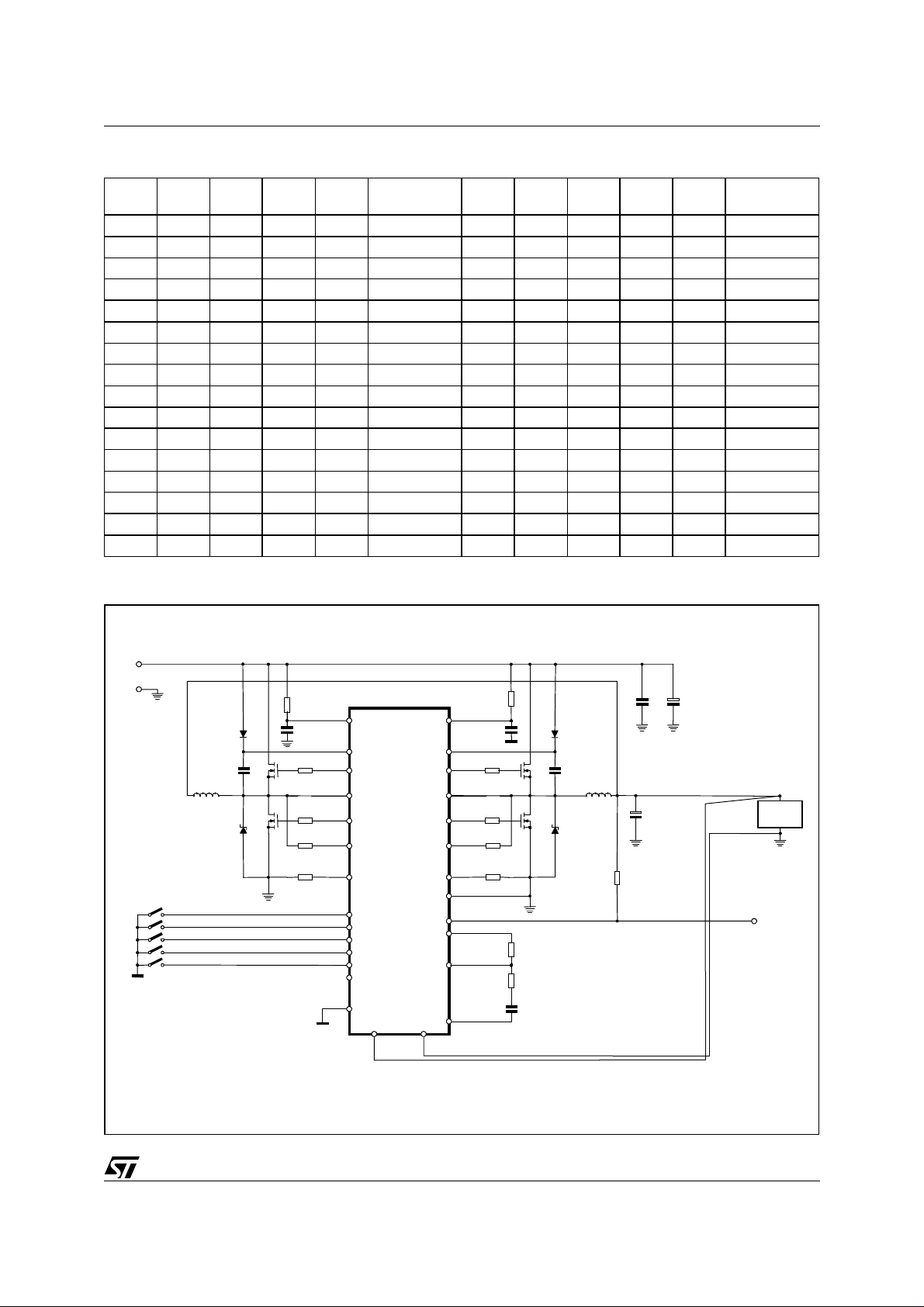
Table 1. Voltage Identification (VID) Codes
VID4 VID3 VID2 VID1 VID0
00000
00001
00010
00011
00100
00101
00110
00111
01000
01001
01010
01011
01100
01101
01110
01111
Output
Voltage (V)
1.550
1.525
1.500
1.475
1.450
1.425
1.400
1.375
1.350
1.325
1.300
1.275
1.250
1.225
1.200
1.175
VID4 VID3 VID2 VID1 VID0
10000
10001
10010
10011
10100
10101
10110
10111
11000
11001
11010
11011
11100
11101
11110
11111
L6919C
Output
Voltage (V)
1.150
1.125
1.100
1.075
1.050
1.025
1.000
0.975
0.950
0.925
0.900
0.875
0.850
0.825
0.800
Shutdown
Reference Schematic
Vin
GNDin
L1
S4
S3
S2
S1
S0
HS1
LS1
C
IN
VCCDR
2
BOOT1
5
UGATE1
4
PHASE1
3
LGATE1
1
ISEN1
PGNDS1
OSC / IN H
SGND
VID4
VID3
VID2
VID1
VID0
13
14
L6919C
22
21
20
19
18
17
7
11 12
FBR FBG
Rg
Rg
VCC
6
BOOT2
24
UGATE2
25
PHASE2
26
LGATE2
27
ISEN2
16
PGNDS2
15
PGND
28
PGOOD
23
VSEN
10
FB
9
COMP
8
HS2
L2
C
LS2
Rg
Rg
R
FB
R
F
C
F
OUT
LOAD
PGOOD
5/32

L6919C
PIN FUNCTION
N Name Description
1 LGATE1 Channel 1 low side gate driver output.
2 VCCDR LS Mosfet driver supply. It can be varied from 5V to 12V.
3 PHASE1 This pin is connected to the source of the upper mosfet and provides the return path for the high
4 UGATE1 Channel 1 high side gate driver output.
5 BOOT1 Channel 1 bootstrap capacitor pin. Through this pin is supplied the high side driver and the upper
6 VCC Device supply voltage. The operative supply voltage is 12V.
7 GND All the internal references are referred to this pin. Connect it to the PCB signal ground.
8 COMP This pin is connected to the error amplifier output and is used to compensate the control
9 FB This pin is connected to the error amplifier inverting input and is used to compensate the voltage
10 VS EN Connected to the outpu t voltage it is able to manage Over&Unde r-voltage conditions and the
11 FBR Remote sense buffer non-inverting input. It has to be connected to the positive side of the load to
side driver of channel 1.
mosfet. Connect through a capacitor to the PHASE1 pin and through a diode to Vcc (cathode vs.
boot).
feedback loop.
control feedback loop.
A current prop ortional to t he su m of the c urren t sen sed i n bot h cha nnel is so urced from this pin
(50µA at full load, 70µA at the 140% Constant Current threshold). Connecting a resistor between
this pin and VSEN pin allows programming the droop effect.
PGOOD signal. It is internally connected with the output of the Remote Sense Buffer for Remote
Sense of the regulated voltage.
If no Remote Sense is implemented, connect it directly to the regulated voltage in order to
manage OVP, UVP and PGOOD.
perform a remote sense.
If no remote sense is implemen ted, conn ect directl y to the output voltage (in this c ase conn ect
also the VSEN pin directly to the output regulated voltage).
12 FBG Remote se nse buffer inverting input. It has to b e connected to the ne gative side of the load to
perform a remote sense.
Pull-down to ground if no remote sense is implemented.
13 ISEN1 Channel 1 current sen se pin. The output current may be sensed acr oss a sense resistor or
This pin has to be connected to the low-side mosfet drain or to
dsON.
I
OCPx
35 µARg⋅
---------------------------=
Rsense
6/32
14
15
PGNDS1
PGNDS2
across the low-side mosfet R
the sense resistor throu gh a resisto r Rg in order to program the over current inter vention for this
phase at 140% as follow:
Where 35µA is the cu rrent o ffset in format ion rela tive to the Over Curre nt cond ition (o ffset at OC
threshold minus offset at zero load).
The net connecting the pin to the sense point must be routed as close as possible to the
PGNDS1 net in order to couple in common mode any picked-up noise.
Channel 1 Power Ground sense pin. The net co nnecting the pin to the sense point must be
routed as close as possible to th e ISEN 1 net in order to couple in com mon m ode any picked-up
noise.
Channel 2 Power Ground sense pin. The net co nnecting the pin to the sense point must be
routed as close as possible to th e ISEN 2 net in order to couple in com mon m ode any picked-up
noise.

L6919C
PIN FUNCTION
(continued)
N Name Description
16 ISEN2 Channel 2 current sen se pin. The output current may be sensed acr oss a sense resistor or
across the low-side mosfet R
This pin has to be connected to the low-side mosfet drain or to
dsON.
the sense resistor throu gh a resisto r Rg in order to program the over current inter vention for this
phase at 140% as follow:
I
OCPx
35µARg⋅
---------------------------=
Rsense
Where 35µA is the cu rrent o ffset in format ion rela tive to the Over Curre nt cond ition (o ffset at OC
threshold minus offset at zero load).
The net connecting the pin to the sense point must be routed as close as possible to the
PGNDS2 net in order to couple in common mode any picked-up noise.
17 OSC/
INH/
FAULT
Oscillator switching frequency pin. C onnecting an external r esistor from this p in to GND, the
external frequency is increased according to the equation:
f
S
200kHz
14.82 10
---------------------------- -+=
R
OSC
6
⋅
kΩ()
Connecting a resistor from this pin to Vcc (12V), the switching frequency is reduced according to
the equation:
f
S
200kHz
12.91 10
---------------------------- -+=
R
OSC
7
⋅
kΩ()
If the pin is not connected, the switching frequency is 200KHz.
Forcing the pin to a voltage lower than 0.6V, the device stop operation and enter the inhibit state.
The pin is forced hig h when an Over/Under Voltage is detected. This cond ition is latched; to
recover it is necessary turn off and on VCC.
18-22 VID4-0 Voltage IDen tification pins. These input are inter nally pulled-up and TTL compa tible. They are
used to program the output voltage as specified in Table 1 and to set the power good thresholds.
Connect to GND to program a ‘0’ while leave floating to program a ‘1’.
23 PGOOD This pin is an open collector output and is pulled low if the output voltage is not within the above
specified thresholds.
If not used may be left floating.
24 BOOT2 Channel 2 bootstrap capacitor pin. Through this pin is supplied the high side driver and the upper
mosfet. Connect through a capacitor to the PHASE2 pin and through a diode to Vcc (cathode vs.
boot).
25 UGATE2 Channel 2 high side gate driver output.
26 PHASE2 This pin is connected to the source of the upper mosfet and provides the return path for the high
side driver of channel 2.
27 LGATE2 Channel 2 low side gate driver output.
28 PG ND Power ground pin. This pin is common to both section s and it must be connected through the
closest path to th e low side mosfets source pins in order to reduce the noise injection into the
device.
7/32
L6919C
DEVICE DESCRIPTION
The device is an i ntegrated circuit r ealized in BCD technol ogy. It provides c omplete control logic and protections
for a high performance dual-phase step-down DC-DC converter optimized for microprocessor power supply. It
is designed to drive N Channel MOSFETs in a dual-phase synchronous-rectified buck topology. A 180 deg
phase shift is provided between the two phases allowing reduction in the input capaci tor current rippl e, reducing
also the size and the losses. The output voltage of the converter can be precisely regulated, programming the
VID pins, from 0.800V to 1.550V with 25mV binary step s, w ith a ma ximum toler ance of ±0.6% over temper ature
and line voltage variations. The device manages On-The-Fly VID Code changes stepping to the new configuration following the VID table with no need for external components. The device provides an average currentmode control with fast transient response. It includes a 200kHz free-running oscillator. The error amplifier features a 15V/
mation is read across the lower mosfets R
information corrects the PW M output in order to equalize the average current carried by each phase. Current
sharing between the two phas es is then li mited at ±10% over stati c and dynamic conditions. The dev ice protects
against Over-Current, with an OC threshold for each phase, entering in constant current mode. Since the curr ent
is read across the low side mosfets, the constant current keeps constant the bottom of the inductors current
triangular waveform. When an under voltage is detected the device latches and the FAULT pin is driven high.
The device performs also Over-Voltage protection that disables immediately the device turning ON the lower
driver and driving high the FAULT pin.
OSCILLATOR
The switchi ng frequ ency i s int ernal ly fixed t o 200 kHz. The i ntern al o scil lator generat es the t riangu lar wave form for t he
PWM charging and dischar ging with a con stant current an internal capacitor. The current delivered to t he oscillator is
typicall y 1 7
GND or Vcc. Since the OSC pin is maintained at fixed voltage (Typ. 1. 235V), the f requency is varied proportionally t o
the current sunk (forced) fro m (into) the pin consider ing the internal gai n of 12KHz/
In particular connecting it to GND the frequency is increased (current is sunk from the pin), while connecting ROSC
to Vcc=12V the frequency is reduced (cur rent is forced into the pin), according to the following relat ionships:
µ
s slew rate that permits high converter bandwidth for fast transient performances. Current infor-
or across a sense resistor in fully differential mode. The current
dsON
µ
A (Fsw=200KHz) a nd may b e vari ed using an ext ernal resi stor ( ROSC) c onnected bet ween OSC pin a nd
µ
A.
vs. GND: f
R
OSC
vs. 12V: f
R
OSC
S
S
200kHz
200kHz
12 1.237
------------------------------
R
1.237
------------------------------
R
OSC
Ω()
K
–
Ω()
K
OSC
kHz
-----------⋅+
12
µ
kHz
-----------
⋅–
12
µ
A
A
200kHz
200kHz
14.82 10
------------------------------+==
R
OSC
12.918 10
--------------------------------–==
R
OSC
⋅
Ω()
K
⋅
Ω()
K
6
7
Note that forcing a 17µA current into this pin, the device stops switching because no current is delivered to the
oscillator.
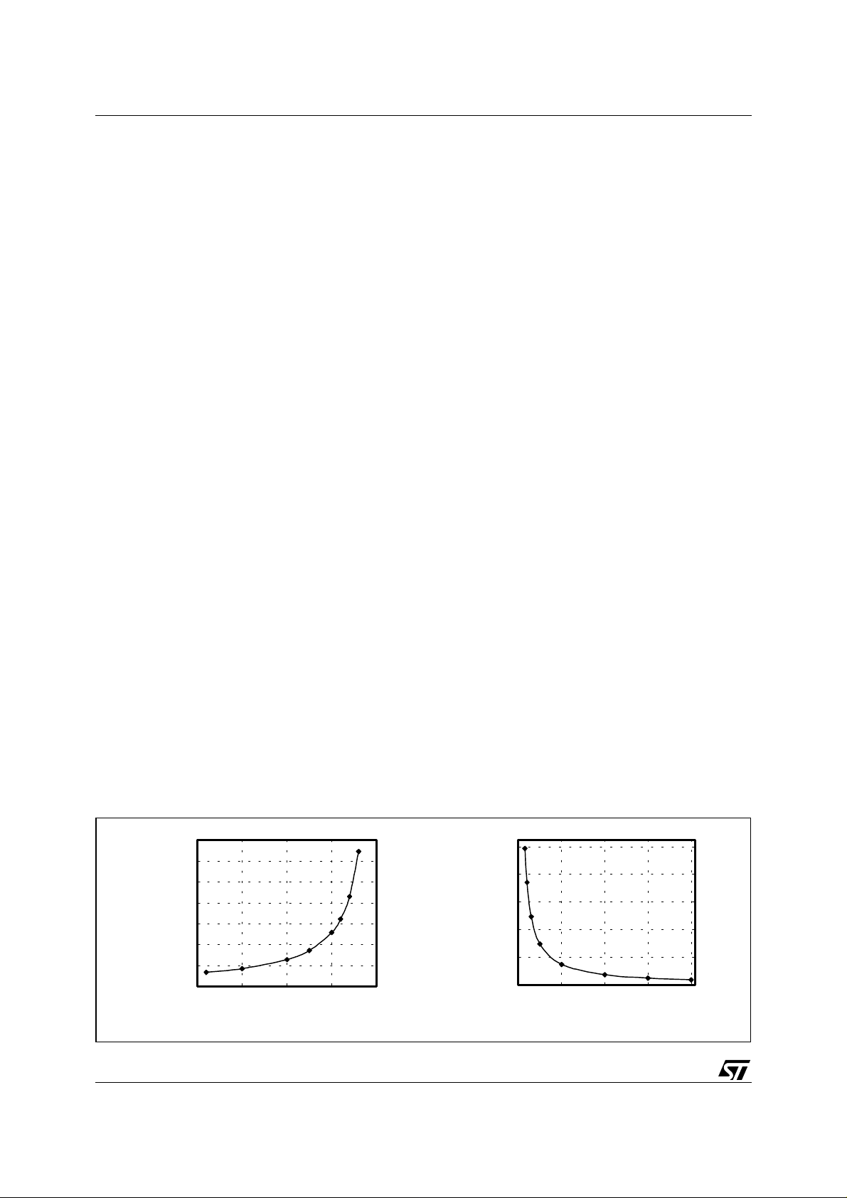
Figure 1. R
vs. Switching Frequency
OSC
7000
6000
5000
4000
) vs. 12V
Ω
3000
2000
Rosc(K
1000
0
0 50 100 150 200
Frequency ( KH z)
1000
800
600
) vs. GND
Ω
400
Rosc(K
200
0
200 300 400 500 600
Freque nc y (KHz)
8/32

L6919C
DIGITAL TO ANA LOG CONVERTER
The built-in digital to analog converter allows the adjustment of the output voltage from 0.800V to 1.550V with
25mV as shown in the previous table 1. The internal reference is trimmed to ensure output voltage precision of
±0.6% and a zero temperature coefficient around 70°C. The internal reference voltage for the regulation is programmed by the voltage identification (VID) pins. T hese are TTL compatible inputs of an internal DAC that is
realized by means of a series of resistors providing a partition of the internal voltage reference. The VID code
drives a multiplexer that selects a voltage on a precise point of the divider. The DAC output is delivered to an
amplifier obtaining the V
provided (realized with a 5
to leave the pin floating, while to program a logic "0" it is enough to short the pin to GND. Programming the
"11111" code, the device en ters the NOCPU mode: all mosfets are turned OFF and protecti ons are diab led. The
condition is latched.
The voltage identification (VID) pin configuration also sets the power-good thresholds (PGOOD) and the Ov er
/ Under Voltage protection (OVP/UVP) thresholds.
DYNAMIC VID TRANSITIO N
The device is able to manage On-The-Fly VID Code changes that allow Output Voltage modification during normal device operation. The device checks every clock cycle (synchronously with the PWM ramp) for VID code
modifications. Once the new code is stable for more than one clock cycle, the reference steps up or down in
25mV increments every c lock cycl e until the new VID code i s reached. Dur ing the tr ansiti on, VID code c hanges
are ignored; the device re-starts monitoring VID after the transiti on has finis hed. P GOOD, signal is masked during the transition and it is re-activated after the transition has finished while OVP / UVP are still active.
voltage reference (i.e. the set-point of the error amplifier). Internal pull-ups are
PROG
µ
A current generator up to 3.3V Typ); in this way, to program a logic "1" it is enough
Figure 2. Dynamic VID transition
VID
Reference
V
OUT
25mV steps transition
1 Clock Cycle Blanking Time
t
t
t
SOFT START AND INHIBIT
At start-up a ramp is generated increasing the loop reference from 0V to the final value programmed by VID in
2048 clock periods as shown in figure 3.
Before soft start, the l ower p ower MOS are turned ON after that VCCDR r eaches 2V (independentl y by V cc value) to discharge the output capacitor and to protect the load from high side mosfet failures. Once soft start begins, the reference is increased; also the upper MOS begins to switch and the output voltage starts to increase
with closed loop regulation. At the end of the digital soft start, the Power Good comparator is enabled and the
PGOOD signal is then driven high (See fig. 3). The Under Voltage comparator enabled when the reference voltage reaches 0.8V. The Soft-Start will not take place, if both VCC and VCCDR pins are not above their own turnon thresholds. During normal operation, if any under-voltage is detected on one of the two supplies the device
shuts down. Forcing the OSC/INH/FAULT pin to a voltage lower than 0.6V (Typ.), the device enters in INHIBIT
mode: all the power mosfets are turned off and protections are disabled.
Setting the I NH pin fr ee, causes the device to restart.
9/32
L6919C
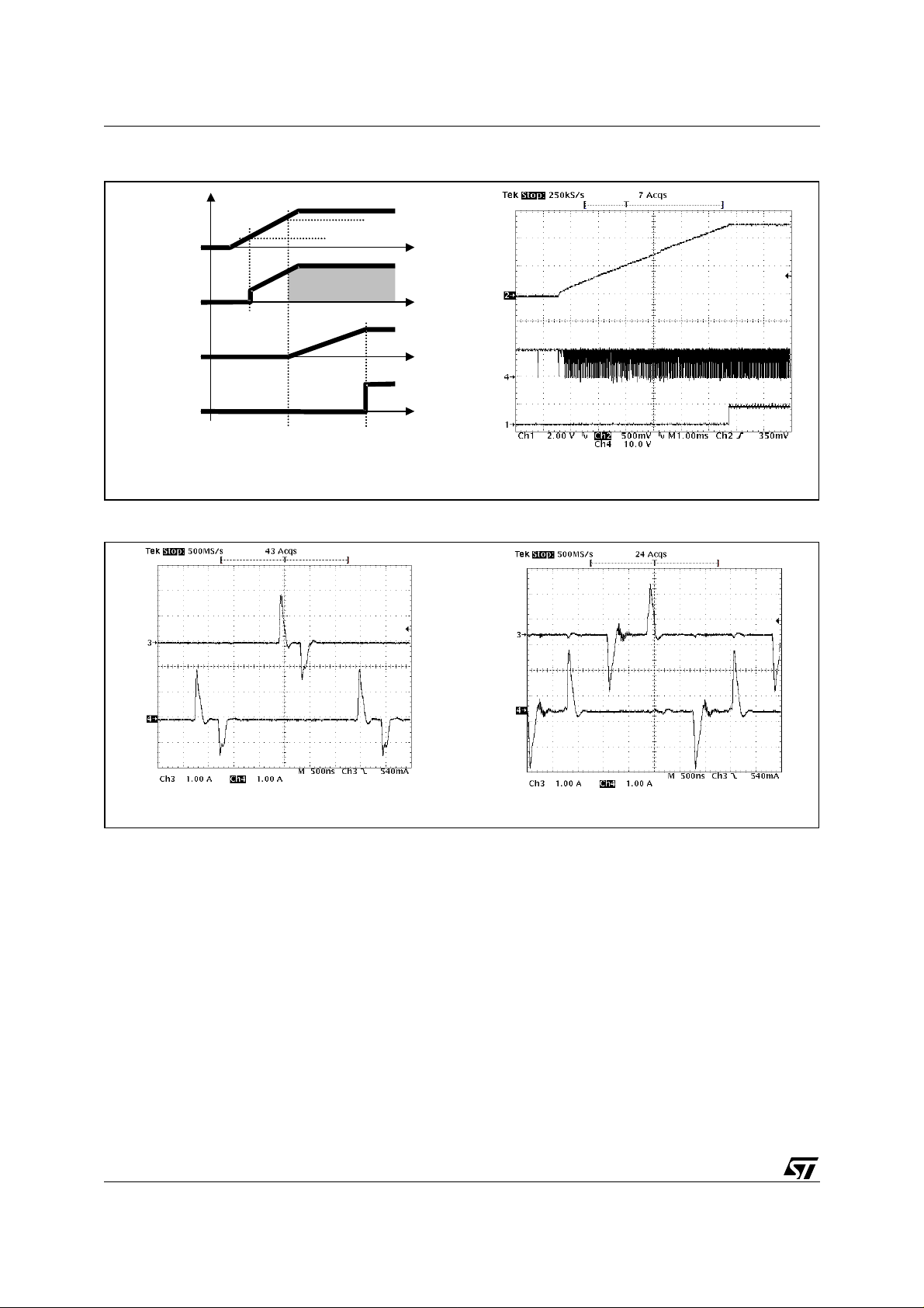
Figure 3. Soft Start
VIN=V
CCDR
V
LGATEx
Turn ON threshold
2V
t
V
PGOOD
OUT
2048 Clock Cycles
Timing Diagram Acquisition:
t
t
t
CH1 = PGOOD; CH2 = V
Figure 4. Drivers peak current: High Side (left) and Low Side (right)
; CH4 = LGATEx
OUT
CH3 = HGATE1; CH4 = HGATE2 CH3 = LGATE1; CH4 = LGATE2
DRIVER SECTION
The integrated high-current drivers allow using different types of power MOS (also multiple MOS to reduce the
R
), maintaining fast switching transition.
dsON
The drivers for the high-side mosfets use BOOTx pins for supply and PHASEx pins for return. The drivers for
the low-side mosfets use VCCDRV pin for supply and PGND pin for return. A minimum voltage of 4.6V at VCCDRV pin is required to start operations of the device.
The controller embodies a sophisticated anti-shoot- through system to minimize low side body diode conduction
time maintaining good efficiency saving the use of Schottky diodes. The dead time is reduced to few nanoseconds assuring that high-side and low-side mosfets are never switched on simultaneously: when the high- side
mosfet turns off, the voltage on its source begins to fall; when the voltage reach es 2V, the low-side mosfet gate
drive is applied with 30ns delay. When the low-side mosfet turns off, the voltage at LGATEx pin is sensed. When
it drops below 1V, the high-side mosfet gate drive is applied with a delay of 30ns. If the current flowing in the
inductor is negativ e, the sourc e of high -side mos f et will nev er dr op. To all ow the tur ning on of the l ow-side mosfet even in this case, a watchdog controller is enabled: if the source of the high-side mosfet don't drop for more
than 240ns, the low side mosfet is switched on so allowing the negative current of the inductor to recirculate.
This mechanism allows the system to regulate even if the current is negative.
10/32
 Loading...