

5 BIT PROGRAMMABLE DUAL-PHASE CONTROLLER
■
2 PHASE OPERATION WITH
SYNCRHONOUS RECTIFIER CONTROL
■
ULTRA FAST LOAD TRANSIENT RESPONSE
■
INTEGRATED HIGH CURRENT GATE
DRIVERS: UP TO 2A GATE CURRENT
■
TTL-COMP A T I BLE 5 BIT P ROGR AMMABLE
OUTPUT CO MPLIANT WITH VRM 9.0
■
0.8% INTERNAL REFERENCE ACCURACY
■
10% ACTIVE CURRENT SHARING
ACCURACY
■
DIGITAL 2048 STEP SOFT-START
■
OVERVOLTAGE PROTEC T I O N
■
OVERCURRENT PROTECTION REALIZED
USING THE LOWER MOSFET'S R
SENSE RESISTOR
■
300 kHz INTERNAL OSCILLATOR
■
OSCILLATOR EXTERNALLY ADJUST ABLE
UP TO 600kHz
■
POWER GOOD OUTPUT AND INHIBIT
FUNCTI ON
■
REMOTE SENSE BUFFER
■
PACKAGE: SO-28
APPLICATION S
■
POWER SUPPLY FOR SERVERS AND
WORKSTATIONS
■
POWER SUPPLY FOR HIGH CURRENT
MICROPROCESSORS
■
DISTRIBUTED DC-DC CONVERTERS
dsON
OR A
L6917B
SO-28
ORDERING NUMB ERS :L691 7BD
L6917BDTR (Tape & Reel)
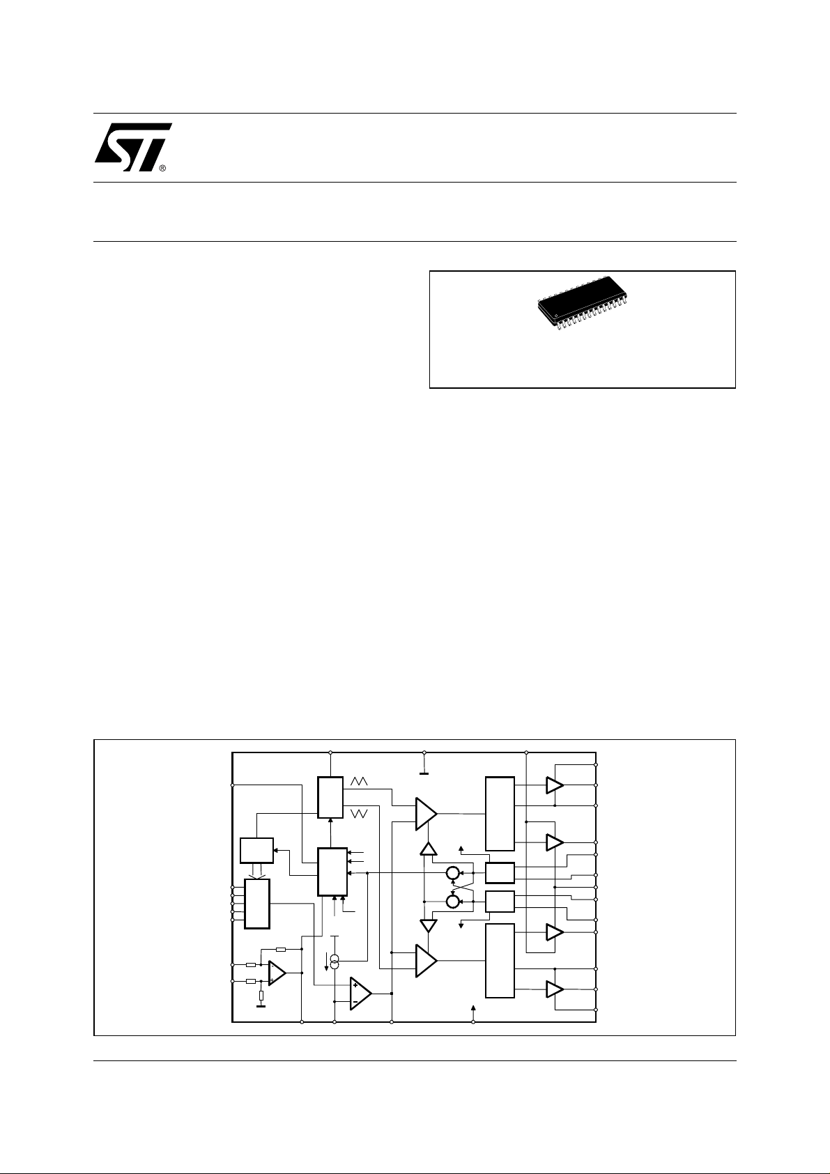
DESCRIPTION
The device is a power supply controller specifically
designed to provide a high performance DC/DC conversion for high current microprocessors.
The device implements a dual-phase step-dow n controller with a 180° phase-shift between each phase.
A precise 5-bit digital to analog converter (DAC) allows adjusting the output voltage from 1.100V to
1.850V with 25mV binary steps.
The high precision internal r eference ass ures the selected output voltage to be within ±0.8%. The high
peak current gate drive affor ds to hav e fast s witching
to the external power mos providing low switching
losses.
The device assures a fast protection against load
over current and load over/under vol t age. An internal
crowbar is provided turning on the low side mosfet if
an over-voltage is detected. In case of over-current,
the system works in Constant Current mode.
BLOCK DIAGRAM
September 2002
PGOOD
VID4
VID3
VID2
VID1
VID0
FBG
FBR
DIGITAL
SOFT START
DAC
10k
10k
10k
10k
REMOTE
BUFFER
VSEN
ROSC / IN H
2 PHASE
OSCILLATOR
LOGIC
AND
PROTECTIONS
CH1 OVER
CURRENT
IFB
FB
CH2 OVER
CURRENT
VCC
VCCDR
ERROR
AMPLIFIER
SGND VCCDR
PWM1
-
+
CH 1 OVER
CURRENT
CURRENT
CORRECT ION
TOTAL
+
CURRENT
AVG
CURRENT
< >
CH 2 OVER
CURRENT
CURRENT
CORRECT ION
+
-
PWM2
LOGIC PWM
ADAPTIVE ANTI
CROSS-CONDUCTION
CURRENT
READING
CURRENT
READING
LOGIC PWM
ADAPTIVE ANTI
CROSS-CONDUCTION
Vcc
VccCOMP
BOOT1
HS
LS
LS
HS
UGATE1
PHASE1
LGATE 1
ISEN1
PGNDS1
PGND
PGNDS2
ISEN2
LGATE 2
PHASE2
UGATE2
BOOT2
1/33

L6917B
T
ABSOLUTE MAXIMUM RATINGS
Symbol Parameter Value Unit
Vcc, V
CCDR
V
BOOT-VPHASE
V
UGATE1-VPHASE1
V
UGATE2-VPHASE2
to PGND 15 V
Boot Voltage 15 V
15 V
LGATE1, PHASE1, LGATE2, PHASE2 to PGND -0.3 to Vcc+0.3 V
All other pins to PGND -0.3 to 7 V
V
phase
Sustainable Peak Voltage t < 20ns @ 600kHz 26 V
THERMAL DATA
Symbol Parameter Value Unit
R
th j-amb
T
T
storage
P
Thermal Resistance Junction to Ambient 60 °C/W
Maximum junction temperature 150 °C
max
Storage temperature range -40 to 150 °C
T
Junction Temperature Range -25 to 125 °C
j
Max power dissipation at T
MAX
= 25°C 2 W
amb
PIN CONNECTION
LGATE1
VCCDR
PHASE1
UGATE1
BOOT1
VCC
GND
COMP
FB
FBR
FBG
ISEN1
PGNDS1
2
3
4
5
6
7
8
9
10VSEN
11
12
13
14
SO28
28
27
26
25
24
23
22
21
20
19
18
17
16
15
PGND1
LGA TE2
PHASE2
UGATE2
BOOT2
PGOOD
VID4
VID3
VID2
VID1
VID0
OSC / INH / FAUL
ISEN2
PGNDS2
2/33

L6917B
ELECTRICAL CHARACTERISTICS
= 12V ±10%, TJ = 0 to 70°C unless otherwise specified
V
CC
Symbol Parameter Test Condition Min Typ Max Unit
Vcc SUPPLY CURRENT
I
I
CCDR
I
BOOTx
Vcc supply current HGATEx and LGATEx open
CC
V
supply current LGATEx open; V
CCDR
Boot supply current HGATEx open; PHASEx to PGND
POWER-ON
Turn-On V
threshold VCC Rising; V
CC
Turn-Off VCC threshold VCC Falling; V
Turn-On V
CCDR
Threshold
Turn-Off V
CCDR
Threshold
OSCILLATOR/INHIBIT/FAULT
f
OSC
f
OSC,Rosc
Initial Accuracy OSC = OPEN
Total Accuracy RT to GND=74kΩ 450 500 550 kHz
INH Inhibit threshold I
d
Maximum duty cycle OSC = OPEN 70 75 %
MAX
V
CCDR=VBOOT
=12V
=12V 2 3 4 mA
CCDR
0.5 1 1.5 mA
7.5 10 12.5 mA
V
CC=VBOOT
V
CCDR
=12V
Rising
=5V 7.8 9 10.2 V
CCDR
=5V 6.5 7.5 8.5 V
CCDR
4.2 4.4 4.6 V
VCC=12V
V
CCDR
Falling
4.0 4.2 4.4 V
VCC=12V
278
OSC = OPEN; Tj=0°C to 125°C
=5mA 0.8 0.85 0.9 V
SINK
270
300 322
330
kHz
kHz
∆Vosc Ramp Amplitude 1.8 2 2.2 V
FAULT Voltage at pin OSC OVP or UVP Active 4.75 5.0 5.25 V
REFERENCE AND DAC
-0.8 - 0.8 %
I
DAC
Output Voltage
Accuracy
VID0, VID1, VID2, VID3, VID4
see Table1;
FBR = V
; FBG = GND
OUT
VID pull-up Current VIDx = GND 4 5 6 µA
VID pull-up Voltage VIDx = OPEN 3.1 - 3.4 V
ERROR AMPLIFIER
DC Gain 80 dB
SR Slew-Rate COMP=10pF 15 V/µs
DIFFERENTIAL AMPLIFIER (REMOTE BUFFER)
DC Gain 1 V/V
CMRR Common Mode Rejection Ratio 40 dB
3/33

L6917B
ELECTRICAL CHARACTERISTICS
V
= 12V ±10%, TJ = 0 to 70°C unless otherwise specified
CC
(continued)
Symbol Parameter Test Condition Min Typ Max Unit
Input Offset F BR=1 .100V to1.850V;
-12 1 2 mV
FBG=GND
SR Slew Rate VSEN=10pF 15 V/µs
DIFFERENTIAL CURRENT SENSING
,
I
ISEN1
I
ISEN2
I
PGNDSx
I
ISEN1
I
ISEN2
I
Bias Current Iload=0 45 50 55 µA
Bias Current 45 50 55 µA
,
Bias Current at
80 85 90 µA
Over Current Threshold
Active Droop Current Iload<0%
FB
Iload=100% 47.5
0
50
1
52.5
GATE DRIVERS
t
RISE
HGATE
I
HGATEx
High Side
Rise Time
High Side
V
BOOTx-VPHASEx
C
V
to PHASEx=3.3nF
HGATEx
BOOTx-VPHASEx
=10V;
15 30 ns
=10V 2 A
Source Current
µA
µA
R
HGATEx
High Side
Sink Resistance
t
RISE
LGATE
I
LGATEx
Low Side
Rise Time
Low Side
Source Current
R
LGATEx
Low Side
Sink Resistance
P GOOD and OVP/UVP PROTECTIONS
PGOOD Upper Threshold
(V
/DACOUT)
SEN
PGOOD Lower Threshold
/DACOUT)
(V
SEN
OVP Over Voltage Threshold
)
(V
SEN
UVP Under Voltage Trip
/DACOUT)
(V
SEN
V
PGOOD
PGOOD Voltage Low I
V
BOOTx-VPHASEx
V
=10V;
CCDR
C
V
V
V
V
V
V
to PGNDx=5.6nF
LGATEx
=10V 1.8 A
CCDR
=12V 0.7 1.1 1.5 Ω
CCDR
Rising 108 112 116 %
SEN
Falling 84 88 92 %
SEN
Rising 2.0 2.25 V
SEN
Falling 56 60 64 %
SEN
= -4mA 0.3 0.4 0.5 V
PGOOD
=12V; 1.5 2 2.5 Ω
30 55 ns
4/33

Table 1. VID Settings
VID4 VID3 VID2 VID1 VID0 Output Voltage (V)
1 1 1 1 1 OUTPUT OFF
11110 1.100
11101 1.125
11100 1.150
11011 1.175
11010 1.200
11001 1.225
11000 1.250
10111 1.275
10110 1.300
10101 1.325
10100 1.350
10011 1.375
L6917B
10010 1.400
10001 1.425
10000 1.450
01111 1.475
01110 1.500
01101 1.525
01100 1.550
01011 1.575
01010 1.600
01001 1.625
01000 1.650
00111 1.675
00110 1.700
00101 1.725
00100 1.750
00011 1.775
00010 1.800
00001 1.825
00000 1.850
5/33

L6917B
PIN FUNCTION
N Name Description
1 LGATE1 Channel 1 low side gate driver output.
2 VCCDR Mosfet driver supply. It can be varied from 5V to 12V.
3 PHASE1 This pin is connected to the source of the upper mosfet and provides the return path for the high
side driver of channel 1.
4 UGATE1 Channel 1 high side gate driver output.
5 BOOT1 Channel 1 bootstrap capacitor pin. Through this pin is supplied the high side driver and the upper
mosfet. Connect through a capacitor to the PHASE1 pin and through a diode to Vcc (cathode vs.
boot).
6 VCC Device supply voltage. The operative supply voltage is 12V.
7 GND All the internal references are referred to this pin. Connect it to the PCB signal ground.
8 COMP This pin is connected to the error amplifier output and is used to compensate the control
feedback loop.
9 FB This pin is connected to the error amplifier inverting input and is used to compensate the voltage
10 VSEN Connected to the output voltage it is able to manage Over & Under-voltage conditions and the
11 FBR Remote sense buffer non-inverting input. It has to be connected to the positive side of the load to
12 FBG Remote sense buffer inverting input. It has to be connected to the negative side of the load to
13 ISEN1 Channel 1 current sense pin. The output current may be sensed across a sense resistor or
14
15
(*) Through a resistor Rg.
PGNDS1
PGNDS2
control feedback loop.
A current proportional to the sum of the current sensed in both channel is sourced from this pin
(50µA at full load, 70µA at the Over Current threshold). Connecting a resistor between this pin
and VSEN pin allows programming the droop effect.
PGOOD signal. It is internally connected with the output of the Remote Sense Buffer for Remote
Sense of the regulated voltage.
If no Remote Sense is implemented, connect it directly to the regulated voltage in order to
manage OVP, UVP and PGOOD.
perform a remote sense.
If no remote sense is implemented, connect directly to the output voltage (in this case connect
also the VSEN pin directly to the output regulated voltage).
perform a remote sense.
Pull-down to ground if no remote sense is implemented.
across the low-side mosfet Rds
This pin has to be connected to the low-side mosfet drain or
ON.
to the sense resistor through a resistor Rg in order to program the positive current limit at 140%
as follow:
35µAR
⋅
I
MAX
--------------------------=
R
g
sense
Where 35µA is the current offset information relative to the Over Current condition (offset at OC
threshold minus offset at zero load).
The net connecting the pin to the sense point must be routed as close as possible to the
PGNDS1 net in order to couple in common mode any picked-up noise.
Channel 1 Power Ground sense pin. The net connecting the pin to the sense point (*) must be
routed as close as possible to the ISEN1 net in order to couple in common mode any picked-up
noise.
Channel 2 Power Ground sense pin. The net connecting the pin to the sense point (*) must be
routed as close as possible to the ISEN2 net in order to couple in common mode any picked-up
noise.
6/33

L6917B
PIN FUNCTION
(continued)
N Name Description
16 ISEN2 Channel 2 current sense pin. The output current may be sensed across a sense resistor or
across the low-side mosfet Rds
This pin has to be connected to the low-side mosfet drain or
ON.
to the sense resistor through a resistor Rg in order to program the positive current limit at 140%
as follow:
35µAR
⋅
I
MAX
--------------------------=
R
g
sense
Where 35µA is the current offset information relative to the Over Current condition (offset at OC
threshold minus offset at zero load).
The net connecting the pin to the sense point must be routed as close as possible to the
PGNDS2 net in order to couple in common mode any picked-up noise.
17
OSC/
INH/
FAULT
Oscillator switching frequency pin. Connecting an external resistor from this pin to GND, the
external frequency is increased according to the equation:
f
S
300KHz
14.82 10
-----------------------------+=
R
OSC
6
⋅
KΩ()
Connecting a resistor from this pin to Vcc (12V), the switching frequency is reduced according to
the equation:
f
S
300KHz
12.91 10
-----------------------------–=
R
OSC
7
⋅
KΩ()
If the pin is not connected, the switching frequency is 300KHz.
Forcing the pin to a voltage lower than 0.8V, the device stop operation and enter the inhibit state.
The pin is forced high when an over or under voltage is detected. This condition is latched; to
recover it is necessary turn off and on VCC.
18-22 VID4-0 Voltage IDentification pins. These input are internally pulled-up and TTL compatible. They are
used to program the output voltage as specified in Table 1 and to set the power good thresholds.
Connect to GND to program a ‘0’ while leave floating to program a ‘1’.
23 PGOOD This pin is an open collector output and is pulled low if the output voltage is not within the above
specified thresholds.
If not used may be left floating.
24 BOOT2 Channel 2 bootstrap capacitor pin. Through this pin is supplied the high side driver and the upper
mosfet. Connect through a capacitor to the PHASE2 pin and through a diode to Vcc (cathode vs.
boot).
25 UGATE2 Channel 2 high side gate driver output.
26 PHASE2 This pin is connected to the source of the upper mosfet and provides the return path for the high
side driver of channel 2.
27 LGATE2 Channel 2 low side gate driver output.
28 PGND Power ground pin. This pin is common to both sections and it must be connected through the
closest path to the low side mosfets source pins in order to reduce the noise injection into the
device.
7/33
L6917B
Device Description
The device is an i ntegrated circuit r ealized in BCD technol ogy. It provides c omplete control logic and protections
for a high performance dual-phase step-down DC-DC converter optimized for microprocessor power supply. It
is designed to drive N Channel MOSFETs in a dual-phase synchronous-rectified buck topology. A 180 deg
phase shift is provided between the two phases allowing reduction in the input capaci tor current rippl e, reducing
also the size and the losses. The output voltage of the converter can be precisely regulated, programming the
VID pins, from 1.100V to 1.850V with 25mV binary step s, w ith a ma ximum toler ance of ±0.8% over temper ature
and line voltage variations. The device provides an average current-mode control with fast transient response.
It includes a 300kHz free-r unning oscil lator adjus table up to 600kH z. The error ampli fier features a 15V/
rate that permits high converter bandwidth for fast transient performances. Current information is read across
the lower mosfets r
or across a sense resistor in fully differential mode. The current information corrects
DSON
the PWM output in order to equalize the average current carried by each phase. Cur rent sharing between the
two phases is then limited at ±10% over static and dynamic conditions. The device protects against over-current, with an OC threshold for each phase, entering in constant current mode. Since the current is read across
the low side mosfets, the constant current keeps constant the bottom of the inductors current triangular waveform. When an under voltage is detected the device latches and the FAULT pin is driven high. The device performs also over voltage pr otection that disable immediately the device turning ON the lower driver and driving
high the FAULT pin.
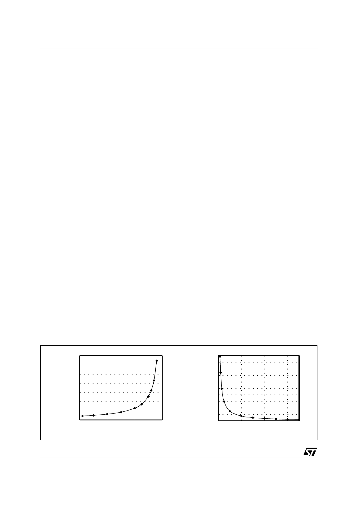
Oscillator
The device has been designed in order to operate an each phase at the same switching frequency of the internal
oscillator. So, input and output resulting frequency is doubled.
The switching frequency is internally fixed to 300kHz. The internal oscillator generates the triangular waveform
for the PWM charging and discharging with a constant c urrent an internal capacit or. The current deliver ed to the
oscillator is typically 25
µ
A and may be varied using an external resistor (R
) connected between OSC pin
OSC
and GND or Vcc. Since the OSC pin is maintained at fixed voltage (typ). 1.235V, the frequency is varied proportionally to the current sunk (forced) from (into) the pin considering the internal gain of 12KHz/
In particular connecting it to GND the frequency is increased (current is sunk from the pin), while connecting ROSC
to Vcc=12V the frequency is reduced (current is forced i nto the pin), accordi ng to the following relationships:
R
OSC
vs. GND: f
S
300kHz
1.237
------------------------------
R
OSC
Ω()
K
12
kHz
-----------⋅+
µ
A
300kHz
14.82 10
------------------------------+==
R
OSC
⋅
K
6
Ω()
µ
s slew
µ
A.
12 1.237
vs. 12V: f
R
OSC
S
300kHz
------------------------------
R
–
OSC
Ω()
K
kHz
-----------
⋅–
12
µ
A
300kHz
12.918 10
--------------------------------–==
R
OSC
⋅
Ω()
K
7
Note that forcing a 25µA current into this pin, the device stops switching because no current is delivered to the
oscillator.
Figure 1. R
) vs. 12V
Ω
Rosc(K
8/33
vs. Switching Frequency
OSC
7000
6000
5000
4000
3000
2000
1000
0
0 100 200 300
Frequency (KH z )
1000
900
800
700
600
) vs. GND
500
Ω
400
300
200
Rosc(K
100
0
300 400 500 600 700 800 900 1000
Frequency (KHz)

L6917B
Digital to Analog Converter
The built-in digital to analog converter allows the adjustment of the output voltage from 1.100V to 1.850V with
25mV as shown in the previous table 1. The internal reference is trimmed to ensure the precision of 0.8% and
a zero temperature coef ficient aroun d 70°C. The inter nal referenc e voltage for the regulation is pr ogrammed by
the voltage identification (VID) pins. These are TTL compatible inputs of an internal DA C that is realized by
means of a series of resistor s providing a parti tion of the inter nal voltage reference. The V ID code drives a multiplexer that selects a voltage on a precise point of the divider. The DAC output is delivered to an amplifier obtaining the VPROG voltage reference (i.e. the set-point of the error amplifier). Internal pull-ups are provided
(realized with a 5
the pin floating, while to program a logic "0" it is enough to short the pin to GND. VID code “11111” programs
the NOCPU state: all mosfets are turned OFF and the condition is latched.
The voltage identification (VID) pin configuration also sets the power-good thresholds (PGOOD) and the overvoltage protection (OVP) thresholds.
Soft Start and INHIBIT
At start-up a ramp is generated increasing the loop reference from 0V to the final value programmed by VID in
2048 clock periods as shown in figure 2.
Before soft start, the lower power MOS are turned ON after that V
to discharge the output capacitor and to protect the load from high side mosfet failures. Once soft start begins,
the reference is increased; when it reaches the bottom of the oscillator triangular waveform (1V typ) also the
upper MOS begins to swi tch and the output volta ge star ts to increase w ith c losed l oop regulation.. At the end of
the digital soft start, the Power Good comparator is enabled and the PGOOD signal is then driven high (See fig.
2). The Under Voltage comparator enabled when the reference voltage reaches 0.8V.
The Soft-Start will not take place, if both V
ing normal operation, if any under-voltage is detected on one of the two supplies the device shuts down.
Forcing the OSC/INH/FAULT pin to a voltage lower than 0.8V the device enter in INHIBIT mode: all the power
mosfets are turned off until this condition is removed. When this pin is freed, the OSC/INH/FAULT pin reaches
the band-gap voltage and the soft start begins.
µ
A current generator up to 3.3V max); in this way, to program a logic "1" it is enough to leave
reaches 2V (independently by Vcc value)
CCDR
and VCCDR pins are not abov e their own turn- on thresholds. Dur-
CC
Figure 2. Soft Start
VIN=V
CCDR
V
LGATEx
V
OUT
PGOOD
Turn ON threshold
2V
t
t
t
2048 Clock Cycles
Timing Diagram Acquisition:
t
CH1 = PGOOD; CH2 = V
; CH4 = LGATEx
OUT
9/33
L6917B
Driver Section
The integrated high-current drivers allow using different types of power MOS (also multiple MOS to reduce the
RDSON), maintaining fast switching transition.
The drivers for the high-side mosfets use BOOTx pins for supply and PHASEx pins for return. The drivers for
the low-side mosfets use VCCDRV pin for supply and PGND pin for return. A minimum voltage of 4.6V at VCCDRV pin is required to start operations of the device.
The controller embodies a sophisticated anti-shoot- through system to minimize low side body diode conduction
time maintaining good efficiency saving the use of Schottky diodes. The dead time is reduced to few nanoseconds assuring that high-side and low-side mosfets are never switched on simultaneously: when the high-side
mosfet turns off, the voltage on its source begins to fall; when the voltage reach es 2V, the low-side mosfet gate
drive is applied with 30ns delay. When the low-side mosfet turns off, the voltage at LGATEx pin is sensed. When
it drops below 1V, the high-side mosfet gate drive is applied with a delay of 30ns. If the current flowing in the
inductor is negativ e, the sourc e of high -side mos f et will nev er dr op. To all ow the tur ning on of the l ow-side mosfet even in this case, a watchdog controller is enabled: if the source of the high-side mosfet don't drop for more
than 240ns, the low side mosfet is switched on so allowing the negative current of the inductor to recirculate.
This mechanism allows the system to regulate even if the current is negative.
The BOOTx and VCCDR pins are separated from IC's power supply (VCC pin) as well as signal ground (SGND
pin) and power ground (PGND pin) in order to maximize the switching noise immunity. The separated supply
for the diff erent drivers gives high flexibility in mosfet choice, allow ing the use of logic- level mosf et. Several combination of supply can be chosen to optimize performance and efficiency of the application. Power conversion
is also flexible, 5V or 12V bus can be chosen freely.
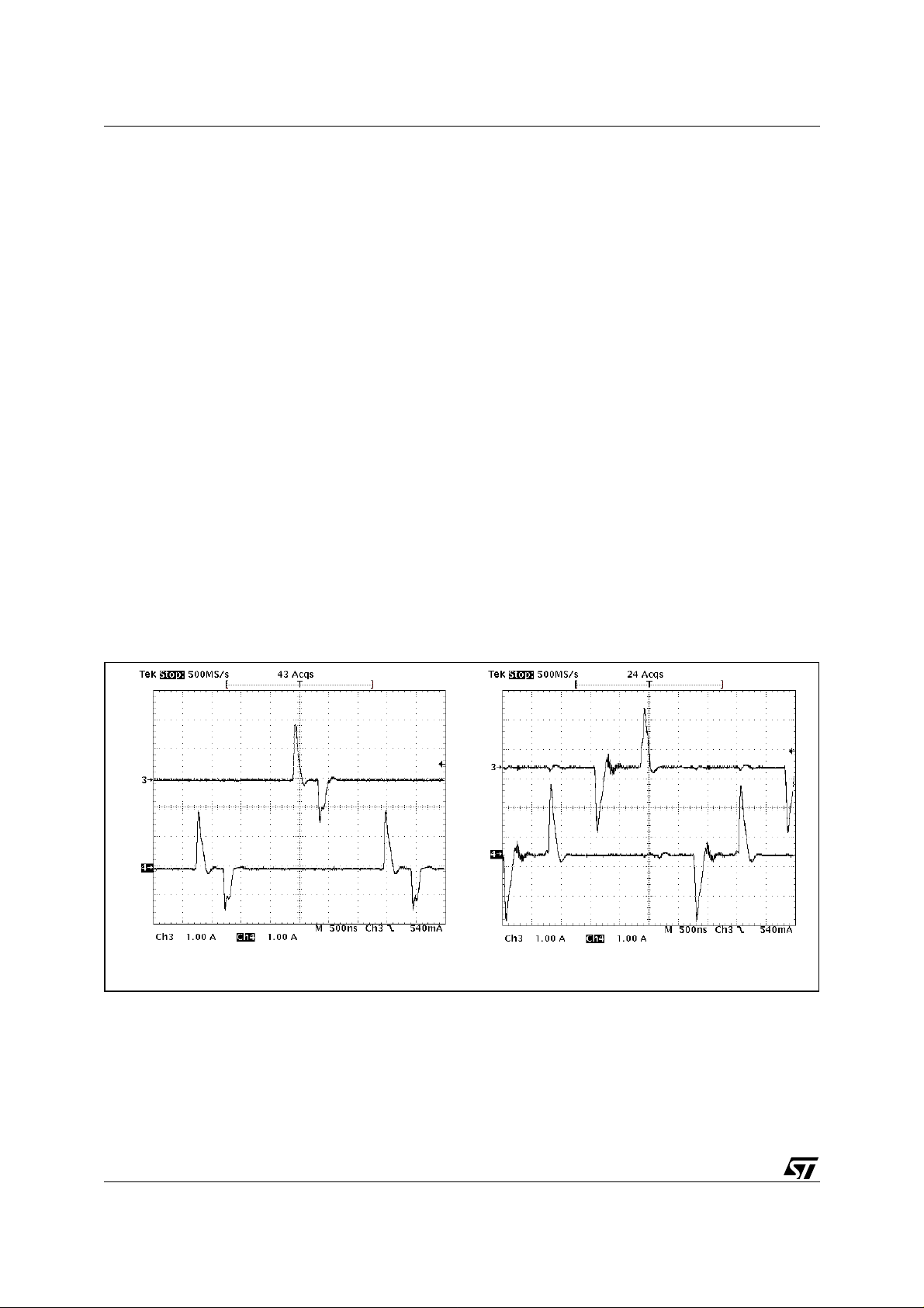
The peak current is shown for both the upper and the lower driver of the two phases in figure 3. A 10nF capacitive load has been used. For the upper drivers, the source current is 1.9A while the sink current is 1.5A with
V
BOOT-VPHASE
VCCDR = 1 2V.
= 12V; similarly, for the lower drivers , the s our ce c urrent is 2.4A while the sink cur rent is 2A w ith
Figure 3. Drivers peak current: High Side (left) and Low Side (right)
CH3 = HGATE1; CH4 = HGATE2 CH3 = LGATE1; CH4 = LGATE2
Current Reading and Over Current
The current flowing trough each phase is read using the voltage drop across the low side mosfets r
across a sense resistor (R
) and internally converted into a current. The transconductance ratio is issued
SENSE
DSON
or
by the external resistor Rg placed outsi de the chip between ISENx and PGNDSx pins toward the reading points.
The full differential current readi ng rejects noi se and allow s to plac e sensing el ement in different lo cations w ithout affecting the measurement's accuracy. The current reading circuitry reads the current during the time in
10/33
 Loading...