

ADJUSTABLE STEP DOWN CONTROLLER
WITH SYNCHRONOUS RECTIFICATION
FEATURE
■ OPER ATING S UPPLY VOLTAGE FROM 5V
TO 12V BUSES
■ UP TO 1.3A GATE CURRENT CAPABILITY
■ ADJUSTABLE OUTPUT VOLTAGE
■ N-INVER TING E/A INPUT AVAILABL E
■ 0.9V ±1.5% VOLTAGE REFERENCE
■ VOLTAGE MODE PWM CONTROL
■ VERY FAST LOAD TRANSIENT RESPONSE
■ 0% TO 100% DUTY CYCLE
■ POWER GOOD OUT PUT
■ OVERVOLTAGE PR OTEC T I O N
■ HICCUP OVERCURRENT PROTECTION
■ 200kHz INTERNAL OSCILLATOR
■ OSCILLATOR EXTERNALLY ADJUSTABLE
FROM 50kHz TO 1MHz
■ SOFT START AND INHIBIT
■ PACKAGES: SO-16 & HTSSOP16
APPLICATIONS
■ SUPPLY FOR MEMORIES AND TERMI-
NATIONS
■ COMPUTER ADD-ON CARDS
■ LOW VOLTAGE DISTRIBUTED DC-DC
■ MAG-AMP RE PL AC EMENT
L6910
L6910A
SO-16 (Narrow) HTSSOP16 (Exposed Pad)
ORDERING NUMBERS:
L6910 (SO-16) L6910A (HTSSOP16)
L6910TR (Tape & Reel) L6910ATR (Tape & Reel)
DESCRIPTION
The device is a pwm controller for high performance
dc-dc conversion from 3.3V, 5V and 12V buses.
The output voltage is adjustable down to 0.9V; higher
voltages can be obtained with an external voltage divider.
High peak current gate drivers provide for fast switching to the external power section, and the output
current can be in excess of 20A.
The device assures protections against load overcurrent and overvoltage. An internal crowbar is also provided turning on the low side mosfet as long as the
over-voltage is detected. In case of over-current detection, the soft start capacitor is discharged and the
system works in HICCUP m ode.
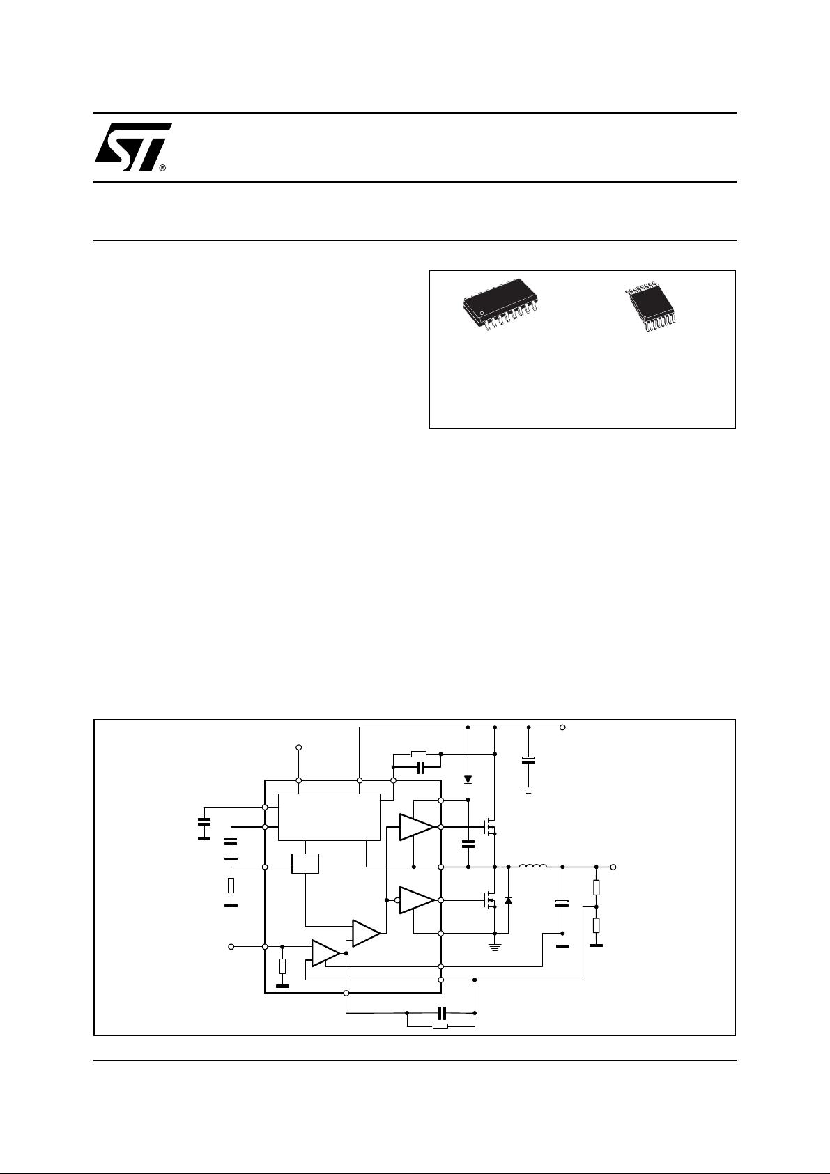
BLOCK DIAGRAM
July 2003
Vin 5V to12V
PGOOD
VCC OCSET
VREF
SS
OSC
RT
EAREF
Monitor
Protec tion and R ef
OSC
L6910
-
+
E/A
+
-
300k
COMP
PWM
BOOT
UGATE
PHASE
LGATE
PGND
GND
VFB
Vo
1/21
L6910A L6910
ABSOLUTE MAXIMUM RATINGS
Symbol Parameter Value Unit
Vcc Vcc to GND, PGND 15 V
V
-
BOOT
V
PHASE
V
HGATE
V
PHASE
Boot Voltage 15 V
-
OCSET, LGATE, PHASE -0.3 to Vcc+0.3 V
SS, FB, PGOOD, VREF, EAREF, RT 7 V
COMP 6.5 V
15 V
T
T
stg
P
tot
Junction Temperature Range -40 to 150 °C
j
Storage temperature range -40 to 150 °C
Maximum power dissipation at Tamb = 25°C1W
THERMAL DATA
Symbol Parameter SO-16 HTSSOP16 HTSSOP16 (*) Unit
R
th j-amb
(*) Device soldered on 1 S2P PC board
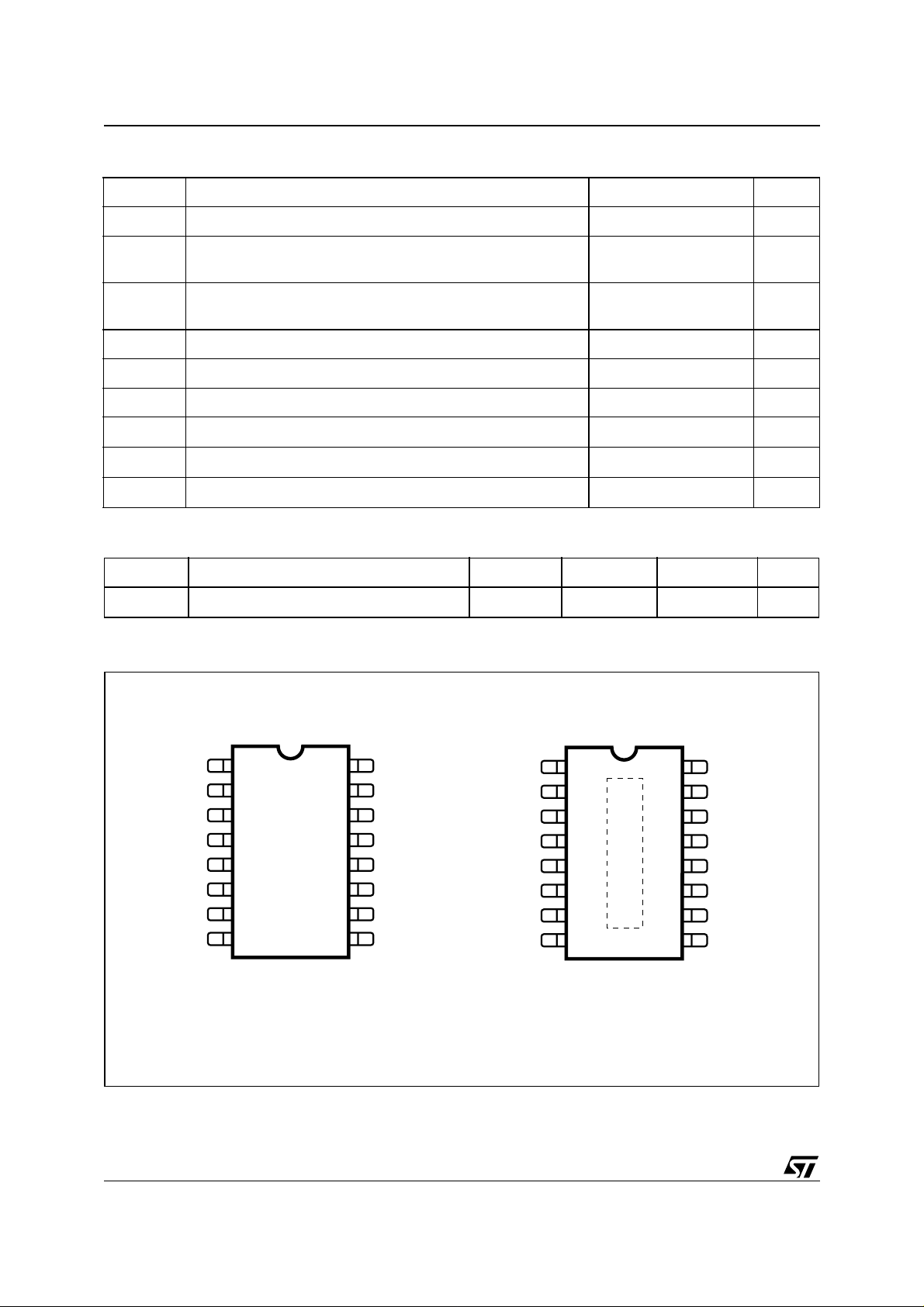
PINS CONNECTION
OCSET
Thermal Resistance Junction to Ambient 120 110 50 °C/W
(Top view)
VREF
OSC
2
3
SS/INH
COMP
FB
GND
EAREF PGOOD
4
5
6
7
8
16
15
14
13
12
11
10
9
SO16
N.C.1
VCC
LGATE
PGND
BOOT
HGATE
PHASE
VREF
OSC
OCSET
SS/INH
N.C.
COMP
FB
GND EAREF
2
3
4
5
6
7
8
HTSSOP-16
16
15
14
13
12
11
10
9
VCC1
LGATE
PGND
BOOT
HGATE
PHASE
PGOOD
2/21

L6910A L6910
PINS FUNCTIO N
SO HTSSOP Name Description
1 1 VREF Internal 0.9V ±1.5% reference is avai lable for external regulator s or for the int ernal erro r
2 2 OSC Oscillator switching frequenc y pin. Connecting a n external resistor (R
3 3 OCSET A resistor connected from this pin and the upper Mos Drain sets the current limit
4 4 SS/INH The soft start time is programmed connecting an external capacitor from this pin and
5 6 COMP This pin is con necte d to the error am plifier out put and is u sed to c ompe nsate the voltag e
6 7 FB This pin is co nnec ted to t he error amplifier inve rting inpu t a nd i s us ed to c ompe nsat e th e
7 8 GND All the internal references are referred to this pin. Connect it to the PCB signal ground.
8 9 EAREF Error amplifier non-inverting inpu t. Conne ct to this pin an ext ernal ref erenc e (from 0.9 V to
910
PGOOD
10 11 PHASE
11 12 HGATE High side gate driver output.
12 13 BOO T Bootstrap c apacitor pin. Through this pi n is supplied the high side driver and the upper
13 14 PGND Power ground pin. This pin ha s to be connec ted closely to the low side m osfet source in
14 ‘5 LGATE This pin is the lower mosfet gate driver output
15 16 VCC Device supply voltage. The operative supply voltage ranges is from 5V to 12V.
16 5 N.C. This pin is not internally bonded. It may be left floating or connected to GND.
amplifier (connecting this pin to EAREF) if external reference is not available.
A minimum 1nF capacitor is required.
If the pin is forced to a voltage lower than 70%, the device enters the hiccup mode.
) from this pin to
T
GND, the external frequency is increased according to the equation:
6
⋅
4.94 10
f
OSC,RT
200KHz
-------------------------+=
RTKΩ()
Connecti ng a resistor (RT) from t his pin to Vcc (12V), the switching frequency is reduce d
according to the equation:
f
OSC,RT
200KHz
4.306 10
---------------------------- -–=
R
KΩ()
T
7
⋅
If the pin is not connected, the switching frequency is 200KHz.
The voltage at this pin is fix ed at 1.23V. Forcing a 50µA current into this pin, the bui lt in
oscillator stops to switch.
In Over Voltage condition this pin goes over 3V until that conditon is removed.
protection.
The internal 200µA current generator sinks a constant current through the external
resistor. The Over-Current threshold is due to the following equation:
I
--------------------------------------------- -=
I
P
⋅
OCSETROCSET
R
DSon
GND. The internal current generator forces through the capacitor 10µA.
This pin can be used to disable the device forcing a voltage lower than 0.4V
control feedback loop.
voltage control feedback loop.
Connected to the outpu t resisto r divide r, if used, or directly to Vout, it manages also ove rvoltage conditions and the PGOOD signal
3V) for the PWM regulation or short it to VREF pin to use the internal reference.
If this pin goes under 650mV (typ), the device shuts down.
This pin is an open collector output and it is pulled low if the output voltage is not within the
above specified thresholds. If not used it may be left floating.
This pin is connected to the source of the upper mosfet and provi des the retur n path for the
high side driver. This pin monitors the drop across the upper mosfet for the current limit
together with OCSET.
mosfet. Connect through a capacitor to the PHASE pin and through a diode to Vcc
(cathode vs. boot).
order to reduce the noise injection into the device
DO NOT CONNECT V
TO A VOLTAGE GREATER THAN VCC.
IN
3/21
L6910A L6910
ELECTRICAL CHARACTERISTICS
(Vcc = 12V, TJ =25°C unless otherwise specified)
Symbol Parameter Test Condition Min Typ Max Unit
V
SUPPLY CURRENT
cc
Icc Vcc Supply current OSC = open; SS to GND 4 7 9 mA
POWER-ON
Turn-On Vcc threshold VOCSET = 4V 4.0 4.3 4.6 V
Turn-Off Vcc threshold VOCSET = 4V 3.8 4.1 4.4 V
Rising V
threshold 1.24 1.4 V
OCSET
Turn On EAREF threshold VOCSET = 4V 650 750 mV
SOFT START AND INHIBIT
Iss Soft start Current
S.S. current in INH condition
SS = 2V
SS = 0 to 0.4V
6103514
60
OSCILLATOR
f
OSC
f
OSC,RT
Initial Accuracy OSC = OPEN
OSC = OPEN; T
= 0° to 125°
j
180
170
Total Accuracy 16 KΩ < RT to GND < 200 KΩ -15 15 %
200 220
230
∆Vosc Ramp amplitude 1.9 V
REFERENCE
V
V
V
Output Voltage Accuracy V
OUT
Reference Voltage C
REF
Reference Voltage C
REF
= VFB; V
OUT
= 1nF; I
REF
= 1nF; TJ = 0 to 125°C-2 +2%
REF
= V
EAREF
REF
REF
= 0 to 100µA 0.886 0.900 0.913 V
0.886 0.900 0.913 V
ERROR AMPLIFIER
I
EAREF
N.I. bias current V
= 3V 10 µA
EAREF
EAREF Input Resistance Vs. GND 300 kΩ
I.I. bias current VFB = 0V to 3V 0.01 0.5 µA
FB
Common Mode Voltage 0.8 3 V
CM
Output Voltage 0.5 4 V
Open Loop Voltage Gain 70 85 dB
V
V
V
COMP
I
G
GBWP Gain-Bandwidth Product 10 MHz
SR Slew-Rate COMP = 10pF 10 V/µs
GATE DRIVERS
I
HGATE
R
HGATE
High Side
Source Current
High Side
V
BOOT
V
HGATE
V
BOOT
- V
- V
- V
= 12V
PHASE
= 6V
PHASE
= 12V 2 4 Ω
PHASE
1 1.3 A
Sink Resistance
I
LGATE
R
LGATE
Low Side Source Current Vcc = 12V; V
Low Side Sink Resistance Vcc = 12V 1.5 3 Ω
= 6V 0.9 1.1 A
LGATE
Output Driver Dead Time PHASE connected to GND 90 210 ns
PROTECTIONS
I
OCSET
I
OSC
OCSET Current Source V
Over Voltage Trip (V
FB
/ V
)VFB Rising 117 120 %
EAREF
OSC Sourcing Current V
= 4V 170 200 230 µA
OCSET
> OVP Trip 15 30 mA
FB
POWER GOOD
V
PGOOD
I
PGOOD
Upper Threshold (V
Lower Threshold (V
Hysteresis (V
FB
PGOOD Voltage Low I
Output Leakage Current V
/ V
/ V
FB
/ V
FB
EAREF
)VFB Rising 108 110 112 %
EAREF
)VFB Falling 88 90 92 %
EAREF
) Upper and Lower threshold 2 %
= -4mA 0.4 V
PGOOD
= 6V 0.2 1 µA
PGOOD
µA
µA
KHz
kHz
4/21

L6910A L6910
Device Description
The device is an integrated circuit realized in BCD technology. The controller provides complete control logic and
protection for a high performance step-down DC-DC converter. It is designed to drive N Channel Mosfets in a
synchronous-rectified buck topology. The output voltage of the converter can be precisely regulated down to
900mV with a maximum tolerance of ±1.5% when the internal reference is used (simply connecting together
EAREF and VREF pins). The device allows also using an external reference (0.9V to 3V) for the regulation. The
device provides voltage-mode control with fast transient response. It includes a 200kHz free-running oscillator that
is adjustable from 50kHz to 1MHz. The error amplifier features a 10MHz gain-bandwidth product and 10V/
rate that permits to realize high converter bandwidth for fast transient performance. The PWM duty cycle can
range from 0% to 100%. The device protects against over-current conditions entering in HICCUP mode. The device monitors the current by using the r
of the upper MOSFET(s) that eliminates the need for a current
DS(ON)
sensing resistor. The device is available in SO16 narrow package.
Oscillator
The switching frequency is internally fixed to 200kHz. The internal oscillator generates the triangular waveform
for the PWM charging and discharging with a constant current an internal capacitor. The current delivered to the
oscillator is typically 50
OSC pin and GND or V
µ
A (Fsw = 200KHz) and may be varied using an external resistor (RT) connected between
. Since the OSC pin is maintained at fixed voltage (typ. 1.235V), the frequency is var-
CC
ied proportionally to the current sunk (forced) from (into) the pin.
In particular connecting R
vs. GND the frequency is increased (current is sunk from the pin), according to the
T
following relationship:
6
⋅
4.94 10
-------------------------+=
R
KΩ()
T
Connecting R
f
OSC,RT
to VCC = 12V or to VCC = 5V the frequency is reduced (current is forced into the pin), according
T
200 KHz
to the following relationships:
7
⋅
f
OSC,RT
200 KHz
4.306 10
---------------------------- -–=
KΩ()
R
T
V
CC
= 12V
µ
s slew
f
OSC,RT
200 KHz
15 1 0
---------------------–=
R
T
Switching frequency variation vs. RT are repeated in Fig. 1.
Note that forcing a 50
µ
A current into this pin, the device stops switching because no current is delivered to the
oscillator.
Figure 1.
10000
1000
100
Resistance [kOhm]
10
10 100 1000
RT to GND
RT to VCC=12V
RT to VCC=5V
Frequency [kHz]
6
⋅
KΩ()
V
= 5V
CC
Reference
A precise ±1.5% 0.9V reference is available. This reference must be filtered with 1nF ceramic capacitor to
avoid instability i n the internal linear regulator. It is
able to deliver up to 100
µ
A and may be used as reference for the device regulation and also for other devices. If forc ed under 70% of it s nominal value, t he
device enters in Hiccup mode until thi s condition is
removed.
Through the EAREF pin the reference for the regulation is taken. This pin directly connect s the non-inverting input of the error amplifier. An external
reference (or the internal 0.9V ±1.5%) may be used.
The input for this pin can range from 0.9V to 3V. It
has an internal pull-down (300k
Ω
resistor) that forces
the device shutdown if no reference is connected (pin
floating). However the device is sh ut dow n if the voltage on the EAREF pin is lower than 650mV (typ).
5/21

L6910A L6910
Soft Start
At start-up a ramp is generated charging the external capacitor CSS with an internal current generator. The initial
value for this current is of 35
10
µ
A until the final charge value of approximatively 4V.
When the voltage across the soft start capacitor (V
charge the output capacitor. As V
MOS begins to switch and the output voltage starts to increase.
No switching activity is observable if SS is kept lower than 0.5V and both mosfets are off.
If VCC and OCSET pins are not above their own turn-on thresholds and V
Start w ill n ot t ake plac e, a n d the re lati ve pin is in ter na lly sho rt ed t o G N D . Du ri ng no rm al o pe rat io n, if a ny undervoltage is detected on one of the two supplies, the SS pin is internally shorted to GND and so the SS capacitor
is rapidly discharged.
Figure 2. Soft Start (with Reference Present)
µ
A and speeds-up the charge of the capacitor up to 0.5V. After that it becames
) reaches 0.5V the lower power MOS is turned on to dis-
reac he s 1. 1 V (i.e . th e os c illato r tri angular wave inferior limit) also the upper
SS
SS
is not above 650mV, the Soft-
EAREF
Vcc
Vin
Vss
LGATE
Vout
to GND
Vcc Turn-on threshold
Vin Turn-on th re s h old
1V
Timing Diagram
0.5V
Acquisition: CH1 = PHASE; CH2 = V
CH3 = PGOOD; CH4 = V
ss
out
;
Driver Section
The driver capability on the high and low side drivers allows using different types of power MOS (also multiple
MOS to reduce the R
), maintaining fast switching transition.
DSON
The low-side mos driver is supplied directly by Vcc while the high-side driver is supplied by the BOOT pin.
Adaptative dead time control is implemented to prevent cross-conduction and allow to use several kinds of mos-
fets. The upper mos turn-on is avoided i f the lower gate i s over about 200mV while the l ower mos turn-on is
avoided if the PHASE pin is over about 500mV. T he l ower mos is i n any cas e turned-on after 200ns from the
high side turn-off.
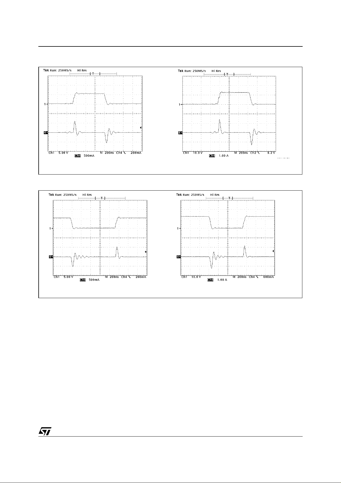
The peak current is shown for both the upper (fig. 3) and the lower (fig. 4) driver at 5V and 12V. A 3.3nF capacitive load has been used in these measurements.
For the lower driver, the source peak current is 1.1A @ V
current is 1.3A @ V
= 12V and 500mA @ VCC = 5V.
CC
= 12V and 500mA @ VCC = 5V, and the sink peak
CC
Similarly, for t he upper dri ver, t he source peak current i s 1. 3A @ Vboot-Vphase = 12V and 600mA @ VbootVphase = 5V, and the sink peak current is 1.3A @ Vboot-Vphase =12V and 550mA @ Vboot-Vpha se = 5V.
6/21
L6910A L6910
Figure 3. High Side driver peak current. Vboot-Vphase = 12V (right) Vboot-Vphase = 5V (left)
CH1 = High Side Gate CH4 = Gate Current
Figure 4. Low Side driver peak curren t. VCC = 12V (right) VCC = 5V (left)
CH1 = Low Side Gate CH4 = Gate Current
Monitoring and Protections
The output voltage is monitored by means of pin FB. If it is not within ±10% (typ.) of the programmed value, the
powergood output is forced low.
The device provides overvoltage protection, when the voltage sensed on pin FB reaches a value 17% (typ.)
greater than the reference the OSC pin is forced high (3V typ.) and the lower driver is turned on as long as the
over-voltage is detected.
Overcurrent protection is performed by the device comparing t he drop across the high side MOS, due t o the
R
, with the voltage across the external resistor (R
DSON
upper MOS. Thus the overcurrent threshold (I
Where the typical value of I
R
(also the variation with temperature) and the minimum value of I
dsON
is 200µA. To calculate the R
OCS
) can be calculated with the following relationship:
P
I
P
) connected between the OCSET pin and drain of the
OCS
R
⋅
OCSIOCS
-------------------------------- -=
R
dsON
value it must be consider ed the maximum
OCS
. To avoid undesirable trigger of
OCS
overcurrent protection this relationship must be satisfied:
7/21
 Loading...