

Single phase PWM controller with PowerGOOD
Features
■ Flexible power supply from 5V to 12V
■ Power conversion input as low as 1.5V
■ 0.8V internal reference
■ 0.8% output voltage accuracy
■ High-Current integrated drivers
■ PowerGOOD output
■ Sensorless and programmable OCP across
Low-Side R
■
OV / UV protections
■ VSEN disconnection protection
■ Oscillator internally fixed at 300kHz
■ LS-LESS to manage pre-bias start-up
■ Adjustable output voltage
■ Disable function
■ Internal Soft-Start
■ VFQFPN 10 package
Applications
dsON
L6728
VFQFPN 10
Description
L6728 is a single-phase step-down controller with
integrated high-current drivers that provides
complete control logic and protection to realize in
a simple way general DC-DC converters by using
a compact VFQFPN 10 package.
Device flexibility allows managing conversions
with power input V
supply voltage ranging from 5V to 12V.
L6728 provides simple control loop with voltage
mode EA. The integrated 0.8V reference allows
regulating output voltages with ±0.8% accuracy
over line and temperature variations. Oscillator is
internally fixed to 300kHz.
as low as 1.5V and device
IN
■ Memory and termination supply
■ Subsystem power supply (MCH, IOCH, PCI...)
■ CPU & DSP power supply
■ Distributed power supply
■ General DC / DC converters
L6728 provides programmable dual level over
current protection as well as over and under
voltage protection. Current information is
monitored across the Low-Side MOSFET RdsON
saving the use of expensive and spaceconsuming sense resistors.
PGOOD output easily provides real-time
information on Output Voltage status, through
VSEN dedicated output monitor.
Table 1. Device summary
Order codes Package Packaging
L6728 VFQFPN 10 Tube
L6728TR VFQFPN 10 Tape & Reel
September 2007 Rev 2 1/32
www.st.com
1

Content L6728
Content
1 Typical application circuit and block diagram . . . . . . . . . . . . . . . . . . . . 4
1.1 Application circuit . . . . . . . . . . . . . . . . . . . . . . . . . . . . . . . . . . . . . . . . . . . . 4
1.2 Block diagram . . . . . . . . . . . . . . . . . . . . . . . . . . . . . . . . . . . . . . . . . . . . . . . 4
2 Pins description and connection diagrams . . . . . . . . . . . . . . . . . . . . . . 5
2.1 Pin descriptions . . . . . . . . . . . . . . . . . . . . . . . . . . . . . . . . . . . . . . . . . . . . . 5
3 Thermal data . . . . . . . . . . . . . . . . . . . . . . . . . . . . . . . . . . . . . . . . . . . . . . . 6
4 Electrical specifications . . . . . . . . . . . . . . . . . . . . . . . . . . . . . . . . . . . . . . 7
4.1 Absolute maximum ratings . . . . . . . . . . . . . . . . . . . . . . . . . . . . . . . . . . . . . 7
4.2 Electrical characteristics . . . . . . . . . . . . . . . . . . . . . . . . . . . . . . . . . . . . . . . 7
5 Device description . . . . . . . . . . . . . . . . . . . . . . . . . . . . . . . . . . . . . . . . . . 9
6 Driver section . . . . . . . . . . . . . . . . . . . . . . . . . . . . . . . . . . . . . . . . . . . . . 10
6.1 Power dissipation . . . . . . . . . . . . . . . . . . . . . . . . . . . . . . . . . . . . . . . . . . . 10
7 Soft start . . . . . . . . . . . . . . . . . . . . . . . . . . . . . . . . . . . . . . . . . . . . . . . . . 11
7.1 Low-Side-Less Start up (LSLess) . . . . . . . . . . . . . . . . . . . . . . . . . . . . . . 11
8 Over current protection . . . . . . . . . . . . . . . . . . . . . . . . . . . . . . . . . . . . . 12
8.1 Over current threshold setting . . . . . . . . . . . . . . . . . . . . . . . . . . . . . . . . . 13
9 Output voltage setting and protections . . . . . . . . . . . . . . . . . . . . . . . . 14
10 Application details . . . . . . . . . . . . . . . . . . . . . . . . . . . . . . . . . . . . . . . . . 15
10.1 Compensation network . . . . . . . . . . . . . . . . . . . . . . . . . . . . . . . . . . . . . . 15
10.2 Layout guidelines . . . . . . . . . . . . . . . . . . . . . . . . . . . . . . . . . . . . . . . . . . . 17
11 Application information . . . . . . . . . . . . . . . . . . . . . . . . . . . . . . . . . . . . . 19
11.1 Inductor design . . . . . . . . . . . . . . . . . . . . . . . . . . . . . . . . . . . . . . . . . . . . . 19
11.2 Output capacitor(s) . . . . . . . . . . . . . . . . . . . . . . . . . . . . . . . . . . . . . . . . . . 20
11.3 Input capacitors . . . . . . . . . . . . . . . . . . . . . . . . . . . . . . . . . . . . . . . . . . . . 20
2/32

L6728 Content
12 20A demo board . . . . . . . . . . . . . . . . . . . . . . . . . . . . . . . . . . . . . . . . . . . 21
12.1 Board description . . . . . . . . . . . . . . . . . . . . . . . . . . . . . . . . . . . . . . . . . . . 24
12.1.1 Power input (Vin) . . . . . . . . . . . . . . . . . . . . . . . . . . . . . . . . . . . . . . . . . . 24
12.1.2 Output (Vout) . . . . . . . . . . . . . . . . . . . . . . . . . . . . . . . . . . . . . . . . . . . . . 24
12.1.3 Signal input (Vcc) . . . . . . . . . . . . . . . . . . . . . . . . . . . . . . . . . . . . . . . . . . 24
12.1.4 Test points . . . . . . . . . . . . . . . . . . . . . . . . . . . . . . . . . . . . . . . . . . . . . . . 24
12.1.5 Board characterization . . . . . . . . . . . . . . . . . . . . . . . . . . . . . . . . . . . . . . 25
13 5A demo board . . . . . . . . . . . . . . . . . . . . . . . . . . . . . . . . . . . . . . . . . . . . 26
13.1 Board description . . . . . . . . . . . . . . . . . . . . . . . . . . . . . . . . . . . . . . . . . . . 28
13.1.1 Power input (Vin) . . . . . . . . . . . . . . . . . . . . . . . . . . . . . . . . . . . . . . . . . . 28
13.1.2 Output (Vout) . . . . . . . . . . . . . . . . . . . . . . . . . . . . . . . . . . . . . . . . . . . . . 29
13.1.3 Signal input (Vcc) . . . . . . . . . . . . . . . . . . . . . . . . . . . . . . . . . . . . . . . . . . 29
13.1.4 Test points . . . . . . . . . . . . . . . . . . . . . . . . . . . . . . . . . . . . . . . . . . . . . . . 29
13.1.5 Board characterization . . . . . . . . . . . . . . . . . . . . . . . . . . . . . . . . . . . . . . 29
14 Mechanical data and package dimensions . . . . . . . . . . . . . . . . . . . . . . 30
15 Revision history . . . . . . . . . . . . . . . . . . . . . . . . . . . . . . . . . . . . . . . . . . . 31
3/32
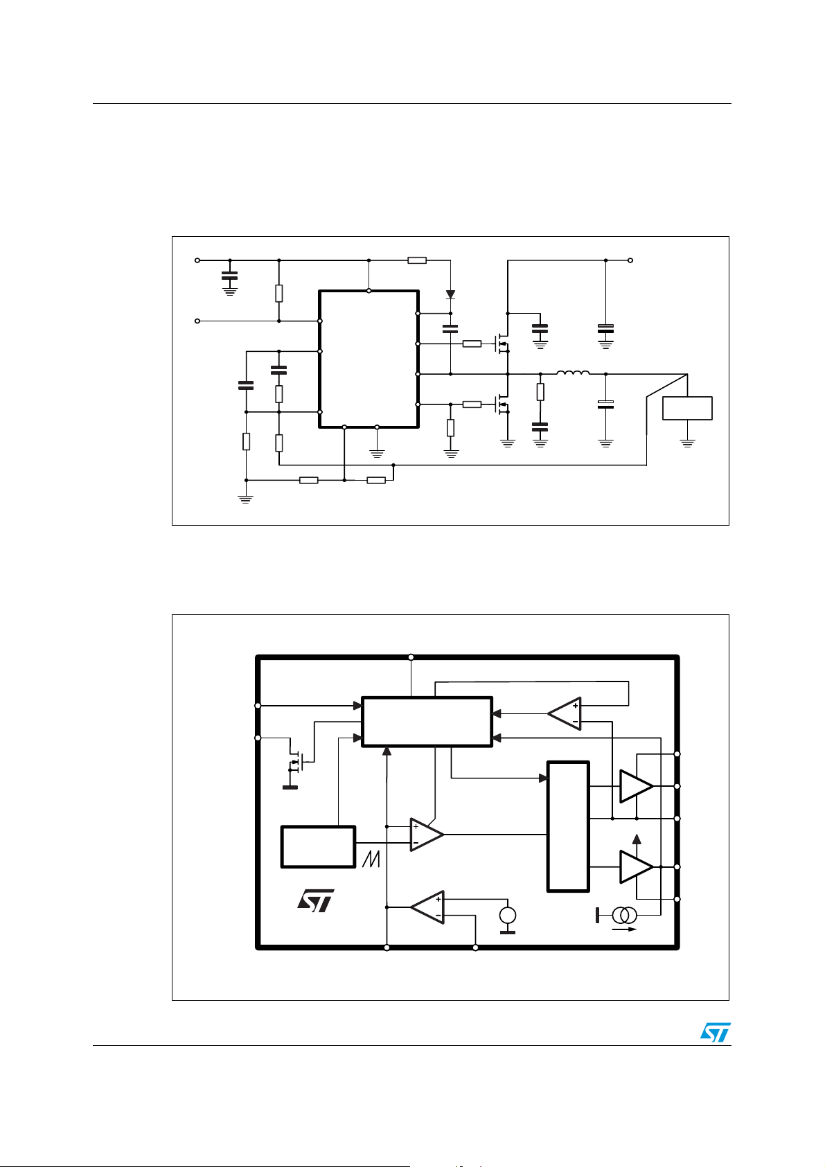
Typical application circuit and block diagram L6728
1 Typical application circuit and block diagram
1.1 Application circuit
Figure 1. Typical application circuit
C
HF
VIN = 1.5V to 12V
L
C
BULK
Vout
C
OUT
LOAD
VCC = 5V to 12V
PGOOD
C
P
R
OS
C
DEC
R
PG
10
PGOOD
7
COMP
C
F
R
F
/ DIS
8
FB
VSEN
R
9
FB
VCC
GND
6
BOOT
UGATE
PHASE
L6728
LGATE
/ OC
5
R
1
3
2
4
OCSET
HS
LS
L6728 Reference Schematic
1.2 Block diagram
Figure 2. Block diagram
V
VSEN
PGOOD
OUT
OSCILLATOR
R
OS
MONITOR
300 kHz
L6728
CLOCK
R
FB
VCC
CONTROL LOGIC
PROTECTIONS
ERROR AMPLIFIER
V
OC
&
OCTH
BOOT
CROSS CONDUCTION
ADAPTIVE ANTI
HS
UGATE
PHASE
PWM
VCC
LS
LGATE
/ OC
GND
+
0.8V
I
OCSET
/ DIS
COMP
4/32
FB
L6728 Pins description and connection diagrams
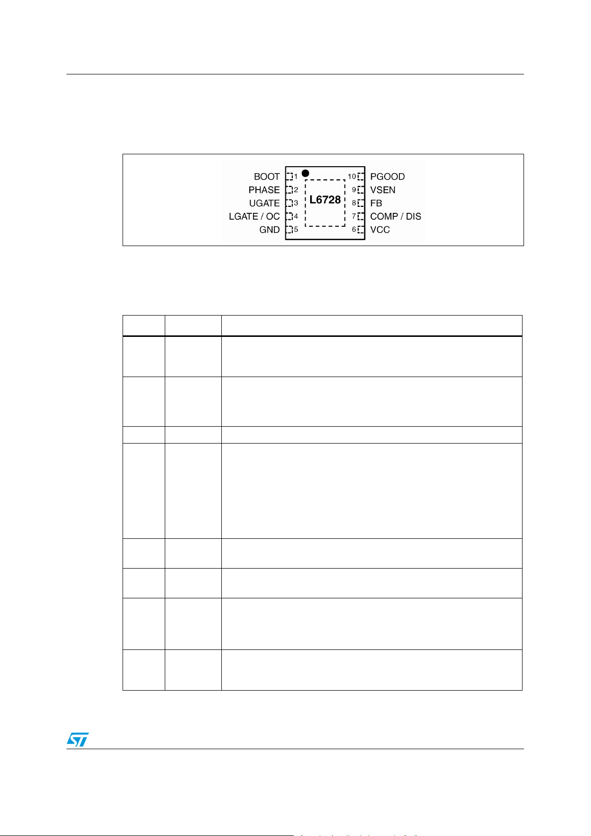
2 Pins description and connection diagrams
Figure 3. Pins connection (top view)
2.1 Pin descriptions
Table 2. Pins description
Pin # Name Function
HS Driver Supply.
1BOOT
Connect through a capacitor (100nF) to the floating node (LS-Drain) pin
and provide necessary bootstrap diode from VCC.
HS Driver return path, current-reading and adaptive-dead-time monitor.
2 PHASE
3 UGATE HS Driver Output. Connect directly to HS MOSFET gate.
4 LGATE / OC
5GND
6VCC
7 COMP / DIS
8FB
Connect to the LS drain to sense RdsON drop to measure the output
current. This pin is also used by the adaptive-dead-time control circuitry to
monitor when HS MOSFET is OFF.
LGATE. LS Driver Output. Connect directly to LS MOSFET gate.
OC. Over Current threshold set. During a short period of time following
VCC rising over UVLO threshold, a 10µA current is sourced from this pin.
Connect to GND with an R
Threshold. The resulting voltage at this pin is sampled and held internally
as the OC set point. Maximum programmable OC threshold is 0.55V. A
voltage greater than 0.6V activates an internal clamp and causes OC
threshold to be set at the maximum value.
All internal references, logic and drivers are connected to this pin.
Connect to the PCB ground plane.
Device and Drivers power supply.
Operative range from 5V to 12V. Filter with at least TBD nF MLCC to GND.
COMP. Error Amplifier Output. Connect with an R
compensate the device control loop.
DIS. The device can be disabled by pushing this pin lower than 0.75V(typ).
Setting free the pin, the device enables again.
Error Amplifier Inverting Input.
Connect with a resistor R
divider may be used to regulate voltages higher than the reference.
FB
resistor greater than 5kΩ to program OC
OCSET
- CF // CP to FB to
F
to the output regulated voltage. Output resistor
5/32
Thermal data L6728
Table 2. Pins description (continued)
Pin # Name Function
Regulated voltage sense pin for OVP and UVP protections and PGOOD.
9 VSEN
Connect to the output regulated voltage, or to the output resistor divider if
the regulated voltage is higher than the reference.
Open Drain Output set free after SS has finished and pulled low when
10 PGOOD
VSEN is outside the relative window. Pull up to a voltage equal or lower
than VCC. If not used it can be left floating.
3 Thermal data
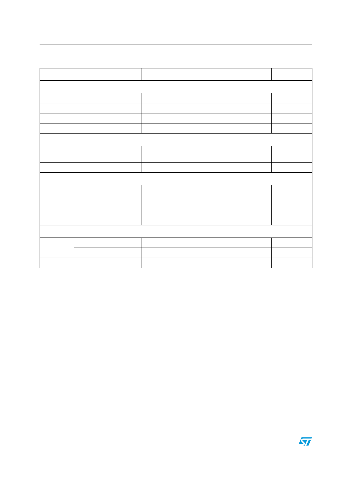
Table 3. Thermal data
Symbol Parameter Value Unit
R
R
T
T
P
th(JA)
th(JC)
MAX
STG
T
J
TOT
Thermal resistance junction to ambient
(Device soldered on 2s2p, 67mm x 69mm board)
45 °C/W
Thermal resistance junction to case 5 °C/W
Maximum junction temperature 150 °C
Storage temperature range -40 to 150 °C
Junction temperature range -40 to 125 °C
Maximum power dissipation at TA = 25°C 2.25 W
6/32
L6728 Electrical specifications
4 Electrical specifications
4.1 Absolute maximum ratings
Table 4. Absolute maximum ratings
Symbol Parameter Value Unit
VCC to GND -0.3 to 15 V
V
BOOT, VUGATE
V
PHASE
V
LGATE
to PHASE
to GND
to GND; t < 200ns
to GND
to GND; t < 200ns
to GND -0.3 to VCC+0.3 V
FB, COMP, VSEN to GND -0.3 to 3.6 V
PGOOD to GND -0.3 to VCC+0.3 V
15
33
45
-5 to 18
-8 to 30
V
V
4.2 Electrical characteristics
Table 5. Electrical characteristics
(V
= 5V to 12V; T
CC
Symbol Parameter Test conditions Min. Typ. Max. Unit
Supply current and power-ON
I
CC
I
BOOT
VCC supply current UGATE and LGATE = OPEN 6 mA
BOOT supply current UGATE = OPEN; PHASE to GND 0.7 mA
VCC Turn-ON VCC Rising 4.1 V
UVLO
Hysteresis 0.2 V
OSCILLATOR
F
∆V
d
SW
OSC
MAX
Main oscillator accuracy 270 300 330 kHz
PWM ramp amplitude 1.4 V
Maximum duty cycle 80 %
Reference and error amplifier
Output voltage accuracy -0.8 - 0.8 %
A
0
DC Gain
(1)
GBWP Gain-bandwidth product
SR Slew-rate
(1)
= 0° to 70°C unless otherwise specified).
j
(1)
120 dB
15 MHz
8V/µs
DIS Disable threshold COMP Falling 0.70 0.85 V
7/32
Electrical specifications L6728
Table 5. Electrical characteristics (continued)
(V
= 5V to 12V; T
CC
Symbol Parameter Test conditions Min. Typ. Max. Unit
Gate drivers
= 0° to 70°C unless otherwise specified).
j
I
UGATE
R
UGATE
I
LGATE
R
LGATE
HS source current BOOT - PHASE = 5V 1.5 A
HS sink resistance BOOT - PHASE = 5V 1.1 Ω
LS source current VCC = 5V 1.5 A
LS sink resistance VCC = 5V 0.65 Ω
Over-current protection
I
OCSET
V
OC_SW
OCSET current source
OC switch-over threshold V
Sourced from LGATE pin, during OC
setting phase.
LGATE/OC
rising 600 mV
91011µA
Over & under-voltage protections
VSEN Rising 0.90 1.00 1.10 V
OVP OVP threshold
un-latch, VSEN Falling 0.35 0.40 0.45 V
UVP UVP threshold VSEN Falling 0.50 0.60 0.70 V
VSEN VSEN bias current Sourced from VSEN 100 nA
PGOOD
Upper threshold VSEN Rising 0.860 0.890 0.920 V
PGOOD
Lower threshold VSEN Falling 0.680 0.710 0.740 V
V
PGOODL
1. Guaranteed by design, not subject to test.
PGOOD Voltage Low I
= -4mA 0.4 V
PGOOD
8/32

L6728 Device description
5 Device description
L6728 is a single-phase PWM controller with embedded high-current drivers that provides
complete control logic and protections to realize in an easy and simple way a general DCDC step-down converter. Designed to drive N-channel MOSFETs in a synchronous buck
topology, with its high level of integration this 10-pin device allows reducing cost and size of
the power supply solution also providing real-time PGOOD in a compact VFQFPN10
3x3mm.
L6728 is designed to operate from a 5V or 12V supply. The output voltage can be precisely
regulated to as low as 0.8V with ±0.8% accuracy over line and temperature variations. The
switching frequency is internally set to 300kHz.
This device provides a simple control loop with a voltage-mode error-amplifier. The erroramplifier features a 15MHz gain-bandwidth product and 8V/µs slew rate, allowing high
regulator bandwidth for fast transient response.
To avoid load damages, L6728 provides over current protection as well as over voltage,
under voltage and feedback disconnection protection. The over current trip threshold is
programmable by a simple resistor connected from Lgate to GND. Output current is
monitored across Low-Side MOSFET R
consuming sense resistor. Output voltage is monitored through dedicated VSEN pin.
, saving the use of expensive and space-
dsON
L6728 implements soft-start increasing the internal reference in closed loop regulation.
Low-Side-Less feature allows the device to perform soft-start over pre-biased output
avoiding high current return through the output inductor and dangerous negative spike at the
load side.
L6728 is available in a compact VFQFN10 3x3mm package with exposed pad.
9/32

Driver section L6728
6 Driver section
The integrated high-current drivers allow using different types of power MOSFET (also
multiple MOSFETs to reduce the equivalent R
The driver for the high-side MOSFET uses BOOT pin for supply and PHASE pin for return.
The driver for low-side MOSFET uses the VCC pin for supply and GND pin for return.
The controller embodies an anti-shoot-through and adaptive dead-time control to minimize
low side body diode conduction time, maintaining good efficiency while saving the use of
Schottky diode:
● to check high-side MOSFET turn off, PHASE pin is sensed. When the voltage at
PHASE pin drops down, the low-side MOSFET gate drive is suddenly applied;
● to check low-side MOSFET turn off, LGATE pin is sensed. When the voltage at LGATE
has fallen, the high-side MOSFET gate drive is suddenly applied.
If the current flowing in the inductor is negative, voltage on PHASE pin will never drop. To
allow the low-side MOSFET to turn-on even in this case, a watchdog controller is enabled: if
the source of the high-side MOSFET doesn't drop, the low side MOSFET is switched on so
allowing the negative current of the inductor to recirculate. This mechanism allows the
system to regulate even if the current is negative.
), maintaining fast switching transition.
dsON
Power conversion input is flexible: 5V, 12V bus or any bus that allows the conversion (See
maximum duty cycle limitations) can be chosen freely.
6.1 Power dissipation
L6728 embeds high current MOSFET drivers for both high side and low side MOSFETs: it is
then important to consider the power that the device is going to dissipate in driving them in
order to avoid overcoming the maximum junction operative temperature.
Two main terms contribute in the device power dissipation: bias power and drivers' power.
● Device Bias Power (P
supply pins and it is simply quantifiable as follow (assuming to supply HS and LS
drivers with the same VCC of the device):
● Drivers power is the power needed by the driver to continuously switch on and off the
external MOSFETs; it is a function of the switching frequency and total gate charge of
the selected MOSFETs. It can be quantified considering that the total power P
dissipated to switch the MOSFETs (easy calculable) is dissipated by three main
factors: external gate resistance (when present), intrinsic MOSFET resistance and
intrinsic driver resistance. This last term is the important one to be determined to
calculate the device power dissipation. The total power dissipated to switch the
MOSFETs results:
) depends on the static consumption of the device through the
DC
P
DC
V
CCICCIBOOT
+()⋅=
SW
P
SW
External gate resistors helps the device to dissipate the switching power since the same
power P
resulting in a general cooling of the device.
10/32
will be shared between the internal driver impedance and the external resistor
SW
F
SW
Q
gHSVBOOT
Q
⋅+⋅()⋅=
gLSVCC
 Loading...