

Feature
■ Flexible power supply from 5V to 12V
■ Power conversion input as low as 1.5V
■ 1% output voltage accuracy
■ High-current integrated drivers
■ Adjustable output voltage
■ 0.8V internal reference
■ Sensorless and programmable OCP across
Low-side R
■
Oscillator internally fixed at 270kHz
■ Programmable soft-start
■ LS-LESS start up
■ Disable function
■ FB disconnection protection
■ SO-8 package
dsON
L6726A
Single phase PWM controller
SO-8
Description
L6726A is a single-phase step-down controller
with integrated high-current drivers that provides
complete control logic, protections and reference
voltage to realize in an easy and simple way
general DC-DC converters by using a compact
SO-8 package.
Device flexibility allows managing conversions
with power input V
supply voltage ranging from 5V to 12V.
as low as 1.5V and device
IN
L6726A provides simple control loop with trans-
Applications
■ Subsystem power supply (MCH, IOCH, PCI...)
■ Memory and termination Supply
■ CPU & DSP power supply
■ Distributed power supply
■ General DC / DC converters
conductance error amplifier. The integrated 0.8V
reference allows regulating output voltage with
±1% accuracy over line and temperature
variations. Oscillator is internally fixed to 270kHz.
L6726A provides programmable over current
protection. Current information is monitored
across the Low-Side mosfet R
saving the use
dsON
of expensive and space-consuming sense
resistors.
FB disconnection protection prevents excessive
and dangerous output voltages in case of floating
FB pin.
Table 1. Device summary
Order codes Package Packaging
L6726A SO-8 Tube
L6726ATR SO-8 Tape & Reel
July 2007 Rev 3 1/24
www.st.com
24

Contents L6726A
Contents
1 Typical application circuit and block diagram . . . . . . . . . . . . . . . . . . . . 4
1.1 Application circuit . . . . . . . . . . . . . . . . . . . . . . . . . . . . . . . . . . . . . . . . . . . . 4
1.2 Block diagram . . . . . . . . . . . . . . . . . . . . . . . . . . . . . . . . . . . . . . . . . . . . . . . 4
2 Pins description and connection diagrams . . . . . . . . . . . . . . . . . . . . . . 5
2.1 Pin descriptions . . . . . . . . . . . . . . . . . . . . . . . . . . . . . . . . . . . . . . . . . . . . . 5
2.2 Thermal data . . . . . . . . . . . . . . . . . . . . . . . . . . . . . . . . . . . . . . . . . . . . . . . 6
3 Electrical specifications . . . . . . . . . . . . . . . . . . . . . . . . . . . . . . . . . . . . . . 7
3.1 Absolute maximum ratings . . . . . . . . . . . . . . . . . . . . . . . . . . . . . . . . . . . . . 7
3.2 Electrical characteristics . . . . . . . . . . . . . . . . . . . . . . . . . . . . . . . . . . . . . . . 7
4 Device description . . . . . . . . . . . . . . . . . . . . . . . . . . . . . . . . . . . . . . . . . . 9
5 Driver section . . . . . . . . . . . . . . . . . . . . . . . . . . . . . . . . . . . . . . . . . . . . . 10
5.1 Power dissipation . . . . . . . . . . . . . . . . . . . . . . . . . . . . . . . . . . . . . . . . . . . 11
6 Soft start and disable . . . . . . . . . . . . . . . . . . . . . . . . . . . . . . . . . . . . . . . 12
6.1 Low-Side-Less start up (LSLess) . . . . . . . . . . . . . . . . . . . . . . . . . . . . . . . 12
6.2 Enable / disable . . . . . . . . . . . . . . . . . . . . . . . . . . . . . . . . . . . . . . . . . . . . 12
7 Protections . . . . . . . . . . . . . . . . . . . . . . . . . . . . . . . . . . . . . . . . . . . . . . . . 13
7.1 Over current protection . . . . . . . . . . . . . . . . . . . . . . . . . . . . . . . . . . . . . . . 13
7.1.1 Over current threshold setting . . . . . . . . . . . . . . . . . . . . . . . . . . . . . . . . 13
7.2 Feedback disconnection protection . . . . . . . . . . . . . . . . . . . . . . . . . . . . . 13
7.3 Under voltage lock out . . . . . . . . . . . . . . . . . . . . . . . . . . . . . . . . . . . . . . . 14
2/24

L6726A Contents
8 Application details . . . . . . . . . . . . . . . . . . . . . . . . . . . . . . . . . . . . . . . . . 15
8.1 Output voltage selection . . . . . . . . . . . . . . . . . . . . . . . . . . . . . . . . . . . . . . 15
8.2 Compensation network . . . . . . . . . . . . . . . . . . . . . . . . . . . . . . . . . . . . . . 15
8.3 Soft Start time calculation . . . . . . . . . . . . . . . . . . . . . . . . . . . . . . . . . . . . 18
8.4 Layout guidelines . . . . . . . . . . . . . . . . . . . . . . . . . . . . . . . . . . . . . . . . . . . 18
8.5 Embedding L6726A-based VRs… . . . . . . . . . . . . . . . . . . . . . . . . . . . . . . 20
9 Package mechanical data . . . . . . . . . . . . . . . . . . . . . . . . . . . . . . . . . . . . 21
10 Revision history . . . . . . . . . . . . . . . . . . . . . . . . . . . . . . . . . . . . . . . . . . . 23
3/24
Typical application circuit and block diagram L6726A
1 Typical application circuit and block diagram
1.1 Application circuit
Figure 1. Typical application circuit
VCC = 5V to 12V
R
R
FB
OS
VIN = 1.5V to 19V
C
DEC
6
FB
7
COMP
C
C
P
R
/ DIS
F
F
3
GND
5
VCC
UGATE
PHASE
L6726A
BOOT
LGATE
/ OC
D
R
D
1
C
BOOT
2
R
R
R
OCSET
gHS
gLS
8
4
HS
LS
C
HF
L
R
SN
C
SN
C
C
(1)
BULK
Vout
OUT
LOAD
L6726A Reference Schematic
(1) Up to 12V with Vcc > 5V
1.2 Block diagram
Figure 2. Block diagram
SS
I
OSCILLATOR
L6726A
VCC
CONTROL LOGIC
& PROTECTIONS
CLOCK
TRANSCONDUCTANCE
ERROR AMPLIFIER
DISABLE
Q
S
R
+
-
OCP
PWM
0.8V
V
OCTH
CROSS CONDUCTION
ADAPTIVE ANTI
I
HS
VCC
LS
OCSET
BOOT
UGATE
PHASE
LGATE
/ OC
GND
/ DIS
COMP
4/24
FB
L6726A Pins description and connection diagrams
2 Pins description and connection diagrams
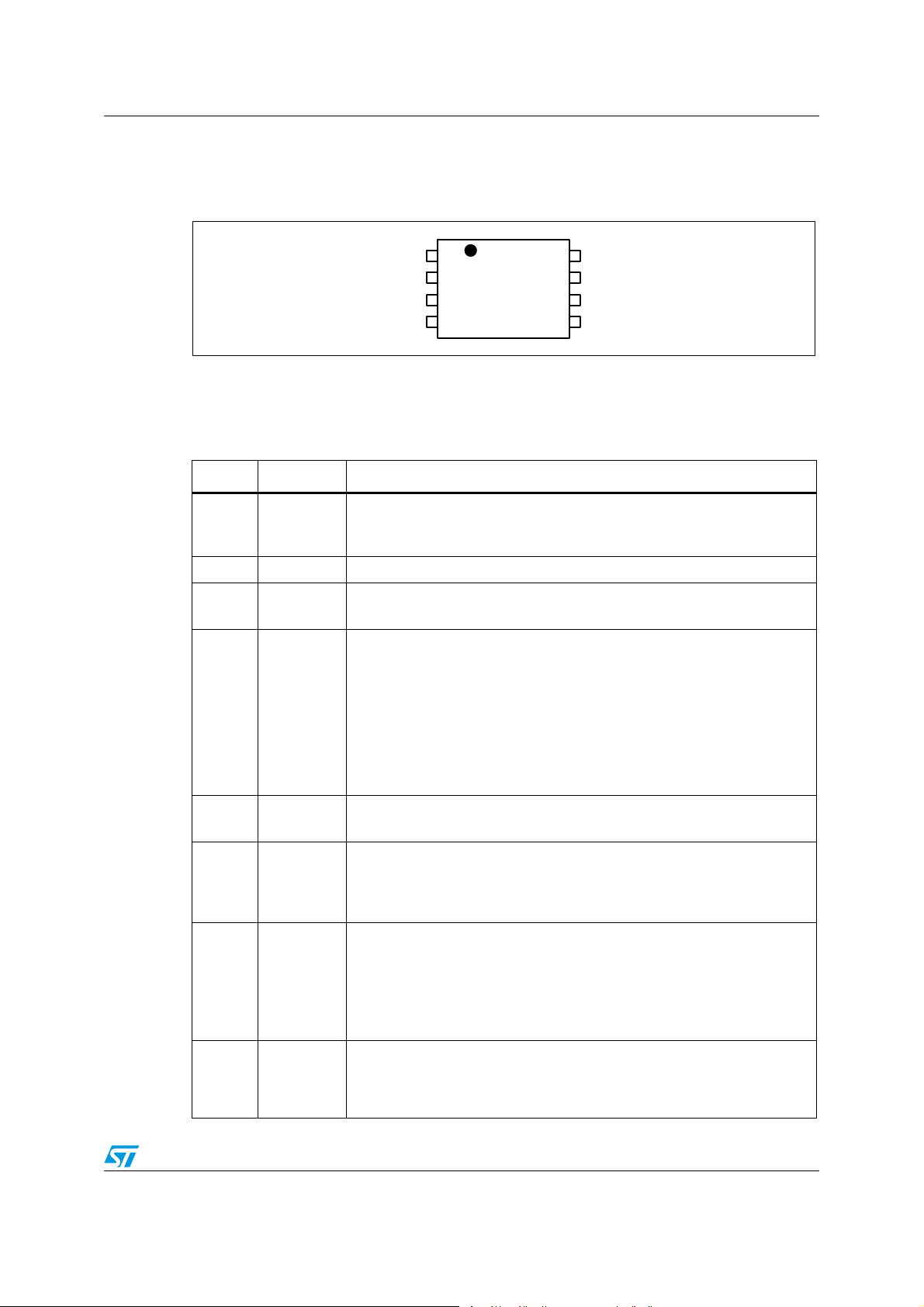
Figure 3. Pins connection (top view)
LGATE / OC
2.1 Pin descriptions
Table 2. Pins descriptions
Pin n Name Function
1BOOT
2 UGATE HS Driver Output. Connect to HS mosfet gate.
3GND
4 LGATE / OC
BOOT
UGATE
GND
HS Driver Supply.
Connect through a capacitor (100nF) to the floating node (LS-Drain) pin
and provide necessary bootstrap diode from VCC.
All internal references, logic and drivers are connected to this pin.
Connect to the PCB ground plane.
LGATE. LS Driver Output. Connect to LS mosfet gate.
OC. Over Current threshold set. During a short period of time following
VCC rising over UVLO threshold, a 10µA current is sourced from this pin.
Connect to GND with an R
Threshold. The resulting voltage at this pin is sampled and held internally
as the OC set point. Maximum programmable OC threshold is 0.55V. A
voltage greater than 0.75V (max) activates an internal clamp and causes
OC threshold to be set at 400 mV. R
default threshold.
1
2
L6726A
3
4
8
PHASE
7
COMP / DIS
6
FB
5
VCC
resistor greater than 5kΩ to program OC
OCSET
not connected sets the 400mV
OCSET
5VCC
6FB
7 COMP / DIS
8 PHASE
Device and LS Driver power supply.
Operative range from 4.1V to 13.2V. Filter with at least 1µF MLCC to GND.
Error Amplifier Inverting Input.
Connect with a resistor R
resistor R
reference.
COMP. Error Amplifier Output. Connect with an R
compensate the device control loop in conjunction to the FB pin.
During the Soft-Start phase, a 10µA current is sourced from this pin so the
compensation capacitors also act to program the SS time.
DIS. The device can be disabled by pulling this pin lower than 0.4V (min).
Setting free the pin, the device enables again.
HS Driver return path, current-reading and adaptive-dead-time monitor.
Connect to the LS drain to sense R
current. This pin is also used by the adaptive-dead-time control circuitry to
monitor when HS mosfet is OFF.
to the output regulated voltage. Additional
to GND may be used to regulate voltages higher than the
OS
FB
- CF // CP to GND to
F
drop to measure the output
dsON
5/24
Pins description and connection diagrams L6726A
2.2 Thermal data
Table 3. Thermal data
Symbol Parameter Value Unit
R
thJA
T
MAX
T
STG
T
J
1. Measured with the component mounted on a 2S2P board in free air (6.7cm x 6.7cm, 35µm (P) and 17.5µm
(S) copper thickness).
Thermal resistance junction to ambient
Maximum junction temperature 150 °C
Storage temperature range -40 to 150 °C
Junction temperature range -20 to 150 °C
(1)
85 °C/W
6/24
L6726A Electrical specifications
3 Electrical specifications
3.1 Absolute maximum ratings
Table 4. Absolute maximum ratings
Symbol Parameter
(1)
Val ue Un it
V
V
BOOT
V
UGATE
V
PHASE
V
LGATE
CC
to GND -0.3 to 15 V
to PHASE
to GND
to PHASE
to PHASE; t < 50ns
to GND
-0.3 to (V
BOOT
V
BOOT
15
45
- V
-1
PHASE)
+ 0.3
+ 0.3
to GND -8 to 30 V
to GND
to GND; t < 50ns
-0.3 to V
-2.5
CC
+ 0.3
FB, COMP to GND -0.3 to 3.6 V
1. ESD immunity for FB pin is guaranteed up to ±1000V (Human Body Model)
3.2 Electrical characteristics
Table 5. Electrical characteristics
(V
= 12V; TA = -20°C to +85°C unless otherwise specified).
CC
Symbol Parameter Test conditions Min. Typ. Max. Unit
Recommended operating conditions
V
CC
V
IN
Device supply voltage
Conversion input voltage
See Figure 1
V
< 7.0V
CC
4.1 13.2 V
13.2 V
19.0 V
V
V
V
Supply current and power-ON
I
CC
I
BOOT
VCC supply current UGATE and LGATE = OPEN 6 mA
BOOT supply current UGATE = OPEN; PHASE to GND 0.5 mA
UVLO VCC Turn-ON VCC Rising 4.1 V
Hysteresis 0.2 V
Oscillator
F
SW
Main oscillator accuracy
T
= 0°C to +70°C 243 270 297
A
225 270 315
∆V
d
OSC
MAX
PWM ramp amplitude 1.1 V
Maximum duty cycle 80 %
7/24
kHz
Electrical specifications L6726A
Table 5. Electrical characteristics (continued)
(V
= 12V; TA = -20°C to +85°C unless otherwise specified).
CC
Symbol Parameter Test conditions Min. Typ. Max. Unit
Reference
V
= 0.8V, TA = 0°C to 70°C -1 - 1
Output voltage accuracy
Transconductance error amplifier
gm Transconductance
I
FB
A
F
I
COMP
0
0
Input bias current Sourced from FB 100 nA
Open loop gain
Unity gain
(1)
Current capability
(1)
(1)
Soft-Start and disable
OUT
= 0.8V -1.5 - 1.5
V
OUT
%
5mS
70 dB
4MHz
Source current 360 µA
Sink current -360 µA
I
SS
Soft-start current From COMP pin 10 µA
DIS Disable threshold COMP falling 0.4 0.5 V
Gate drivers
I
UGATE
R
UGATE
I
LGATE
R
LGATE
HS source current BOOT - PHASE = 5V to 12V 1.5 A
HS sink resistance BOOT - PHASE = 5V to 12V 1.1 Ω
LS source current VCC = 5V to 12V 1.5 A
LS sink resistance VCC = 5V to 12V 0.65 Ω
Over-current protection
I
OCSET
V
OC_SW
V
OCTH_FIXED
1. Guaranteed by design, not subject to test.
OCSET current source
OC switch-over threshold V
Fixed OC threshold V
Sourced from LGATE pin.
See Section 7.1.1
LGATE/OC
PHASE
rising 780 mV
to GND -400 mV
10 µA
8/24
 Loading...