

®
90V BCD MIXED TECHNOLOGY
SO24 PLASTIC SMD PACKAGE
4.5 TO 13.2V OPERATIVE VOLTAGE
±25 TO ±35V OUTPUT VOLTAGE RANGE
SELECTABLE BY EXTERNAL RES ISTO RS
FULL-WAVE RESONANT DC-DC CON-
VERTER USING SINGLE COIL FOR DUAL
HIGH VOLTAGE GENERATOR WITH OUTPUT SLEW RATE CONTROL AND SELF
CURRENT LIMITING FOR LOW EMI
±35V OR 0/+70V OPERATIVE VOLTAGE
DRIVING CONFIGURATION MODES:
1. SINGLE ENDED VOLTAGE MODE
2. DIFFERENTIAL VOLTAGE MODE
3. SINGLE ENDED CHARGE MODE
DOUBLE OPERATIONAL AM PLIFIERS WITH
500KHZ GAIN BANDWIDTH PRODUCT AND
LOAD DRIVING CAPABILITY FROM 0.4nF
UP TO 24nF
ANALOG VOLTAGE SHIFTING CIRCUITRY
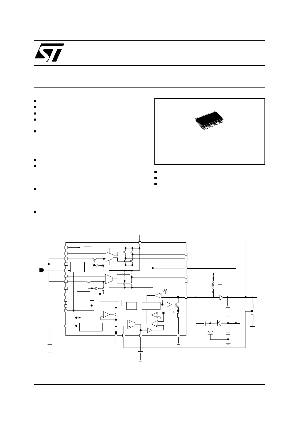
L6660
MILLI-ACTU A TO R DR IVER
PRODUCT PREVIEW
SO24(Shrink)
INTERNAL 2.5V VOLTAGE REFERENCE
POWER SAVING SLEEP MODE
USER SPECIFIED INPUT REFERENCE
(2.25V DC)
DESCRIPTION
The L6660 is a piezoelectric actuator driver.
BLOCK AND APPLICATION DIAGRAM
HVP
-
B
+
HVM
HVP
-
A
+
HVM
A-GND
Internal
Current
Bias
+
-
[12] GND-A [21] Vfdb [22] RCcomp [2] GND-P
From DAC
OUTPUT
[7] SLEEP
[17] INB(inv)
[16] INB(not inv)
[10] Vosh
[11] Vin0-5
[8] INA(inv)
[9] INA(not inv)
[15] WENA
[4] AorB
[1] AandB
[20] V5/12AP
[14] IN Vref
[13] Vref out
100nF
Shifter
Vosh=Vin-Vref
Controll
SLEEP
MUX
Logic
Digital
Pwr Supply
Internal Band-gap
and 2.5 reference Voltage
1
1
1
1
Back-Up
Oscill.
[24] HVP
K
K
K
K
DC-DC LOGIC
V5/12
[18] OUTK-B
[19] OUT1-B
[23] HVM
[6] OUTK-A
[5] OUT1-A
[3] COIL
V512
47µH
2.2nF
+35V
Rfdb1
220nF
Rs
:5
68nF
HVM
-35V
Rfdb2
220nF
47nF
HVP=VrefIN(1+Rfdb1/Rfdb2)
December 2000
This is preliminary information on a new product now in development. Details are subject to change without notice.
1/9
L6660
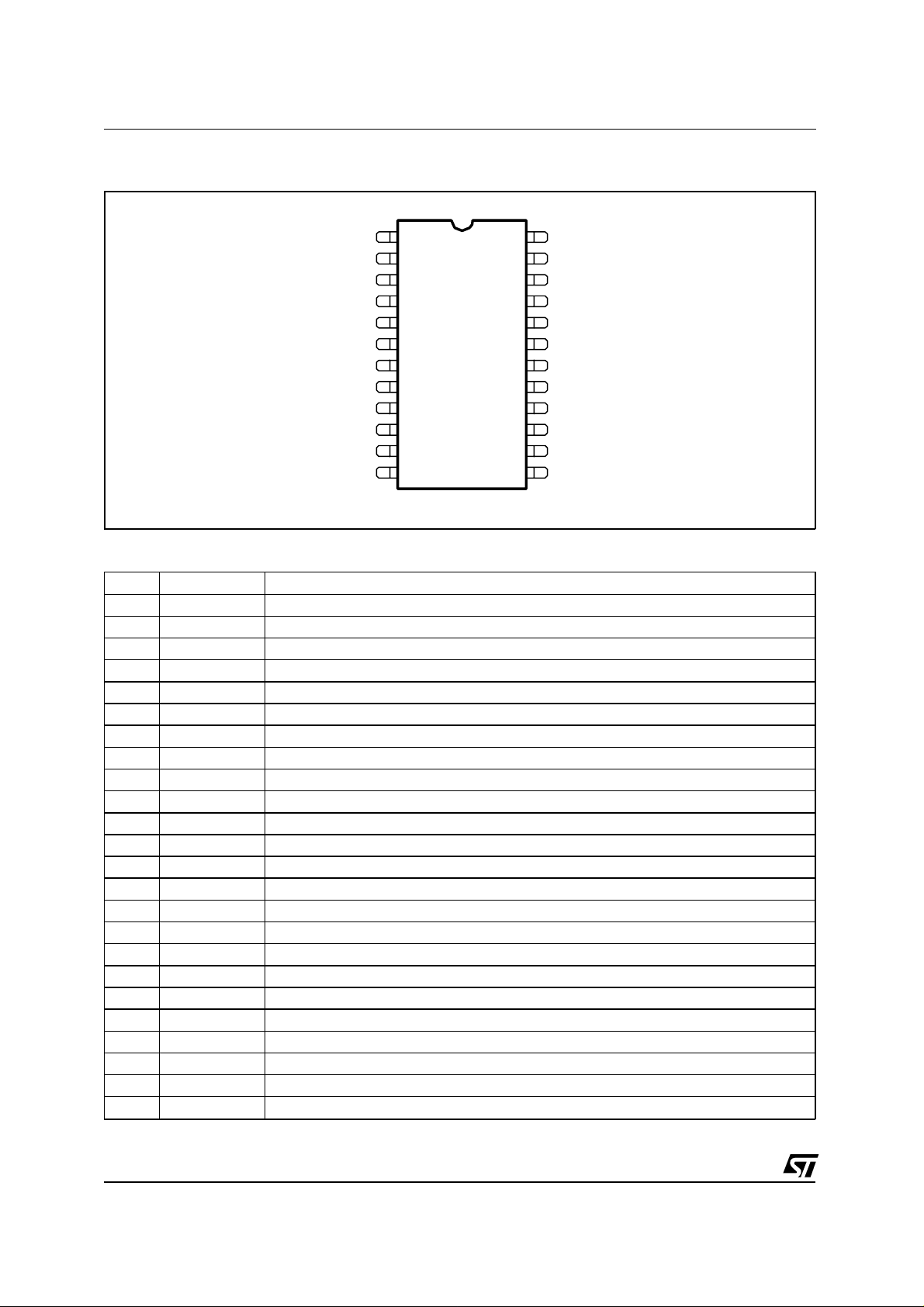
PIN CONNECTION SO24-SHIRINK (Top view)
A and B
GND-P
COIL
A or B.
OUT1-A
OUTK-A
SLEEP
INA(inv)
INA(not inv) INB(not inv)
V
OSH
Vin 0-5 Vref IN11 14
2
3
4
5
6
7
8
9
10
PINCON
24
23
22
21
20
19
18
17
16
15
1312GND-A V ref OUT
HVP1
HVM
RC comp
V
FDB
V5/12-AP
OUT1-B
OUTK-B
INB(inv)
WENA
PIN FUNCTIONS
N. Name Description
1 AandB MUX Enable (see Tab. 1).
2 GND-P Power ground.
3 COIL Coil for positive step UP and capacitor for negative charge.
4 AorB MUX command Aor B input selection (0 = A; 1 = B).
5 OUT1-A Output ampl.A.
6 OUTK-A Hi current output ampl.A.
7 SLEEP Sleep mode for stand-by condition (0=SLEEP 1=operative).
8 INA (inv) Inverting input of A-amplifier.
9 INA (not inv) Non Inverting input of A-amplifier.
10 Vosh Analog level shifter output Vin-Vref (-2.5 to +2.5 dynamic range)
11 Vin 0-5 Analog level shifter input positive voltage.
12 GND-A Analog ground.
13 V
14 V
15 WENA Multiplexer Enable, Falling Edge sensitive.
16 INB (not inv) Non Inverting input of B-amplifier.
17 INB (inv) Inverting input of B-amplifier.
18 OUTK-B Hi current output ampl.B.
19 OUT1-B Output ampl.B.
20 V5/12-AP Analog&Power voltage supply 5 to 12V.
21 Vfdb Feedback voltage for HVP regulator.
22 RC comp DC-DC converter compensation network.
23 HVM Negative High voltage generated op. amp. supply.
24 HVP Positive High voltage generated op. amp. supply.
OUT Precise 2.5V reference voltage.
ref
IN Input for external reference voltage.
ref
2/9
L6660
ABSOLUTE MAXIMUM RATINGS
Symbol Parameter Value Unit
V512 Supply voltage pin 17 referred to Ground 14 V
HVP Positive high voltage referred to HVM 75 V
HVM Negative high voltage referred to Ground -38 V
IN A&B Amplifier input voltage common mode
V Maximum difference between pin 20 and pins 8, 9, 16 & 17 17 V
∆
T
amb
T
stg
All the voltage value are referred to ground unless otherwi se spec i fied.
Operative Ambient Temperature -20 to +80 °C
Storage Temperature -40 to +125 °C
ELECTRICAL CHARACTERISTICS
(All the following parameters are specified @ 27°C and V5/12 = 12V ±5%, unless otherwise specified.)
Symbol Parameter Test Condition Min. Typ. Max. Unit
V
5/12
HVP
HVripple HVP, HVM ripple
I, hvp Output current (see figure 1)
I, hvm
T
op
F
switch
R
ds, on
I
boost
V
sup
DC gain OpAmp DC gain 130 dB
GBW OpAmp Gain Bandwidth
DCinp OpAmp Input dynamic voltage Double supply -3.5 4.5 V
V
out
DC, I
I
(3) OpAmp Dynamic Output
out
PSRR,P OpAmp Positive power supply
PSRR,N OpAmp Negative power supply
C
load
C
int
K OpAmp Current ratio
Main power supply 4.5 13.2 V
(1)
Output positive Voltage Double Supply Voltage V
Double Supply Voltage V
Single Supply Voltage V
Single Supply Voltage V
512
512
512
512
≥ 8
< 8
≥ 8
< 82718
27
18
External filter cap. 100nF
Characterized only, Not Tested
Time to operating condition 5 ms
(2)
Switching Frequency Refer to Block diagram
I
= 0mA 0.8 V
LOAD
page1/10
Boost transistor ON resistance 4
Boost transistor current limiting 850 mA
Minimum OpAmp supply
Voltage (HVP if externally
given)
Double Supply V512
+4
Single Supply V512
+4
Cload 0.4nF to 24nF
product
Double Supply Voltage
Single supply 1.2 5 V
OpAmp Output dynamic voltage Capacitive load HVM HVP V
OpAmp Bias supply current
bias
|HVP| = |HVM| = 35V 9 mA
(both)
-75 +75 mA
Average current with external
supply
@ 50kHz not tested in production -50 dB
rejection ratio
@ 50kHz not tested in production -50 dB
rejection ratio
OpAmp Load capacitance
Voltage mode Gain min 20dB 0.4 24 nF
range
OpAmp Integration capacitance Charge mode Gain min 20dB 0.4 24 nF
9.8 10 10.2
OUTK/OUT1
6V
±
35
35
70
35
V
V
V
V
300 kHz
Ω
V
V
500 KHz
3/9
 Loading...