

SGS Thomson Microelectronics L6611N, L6611D, L6611DTR Datasheet
DIGITALLY PROGRAMMABLE SECONDARY
■
OV/UV DETECTION FOR 3.3V, +5V, ±12V
RAILS AND 5V (OR 3.3V) AUX. VOLTAGE
■
AC MAINS UV (BROWNOUT) DETECTION
WITH HYSTERESIS
■
ON-LINE DIGITAL TRIMMING FOR 5V/12V,
3.3V, 5V (OR 3.3V) AUX. FEEDBACK
REFERENCES AND AC MAINS UV.
■
DIGITALLY SEL EC T ABL E OPT IO N S
■
ERROR AMPLIFIERS FOR 5V/12V RAILS
(MAIN SUPPLY), 3V3 POST-REGULAT OR
(MAG_AMP OR LINEAR) AND AUXILIARY
SUPPLY.
■
MAIN SUPPLY ON/OFF CONTROL AND
POWER GOOD SIGNAL
■
50mA CROWBAR DRIVE FOR AUXIL IARY
OUTPUT OVP .
■
OPEN GROUND PROTEC TI ON
■
8ms DIGITAL SOFT START
■
64 ms UV/OC BLANKING AT START-UP
L6611
HOUSEKEEPING CONTROLLER
BCD TECHNOLOGY
DIP20 SO20
ORDERING NUMBERS:
L6611N L6611D
L6611DTR(T & Reel)
APPLICATION S
■
SWITCHING POWER SUPPLIES FOR
DESKTOP PC'S, SERVERS AND WEB
SERVERS
■
SUPERVISOR FOR DISTRIBUTED POWER
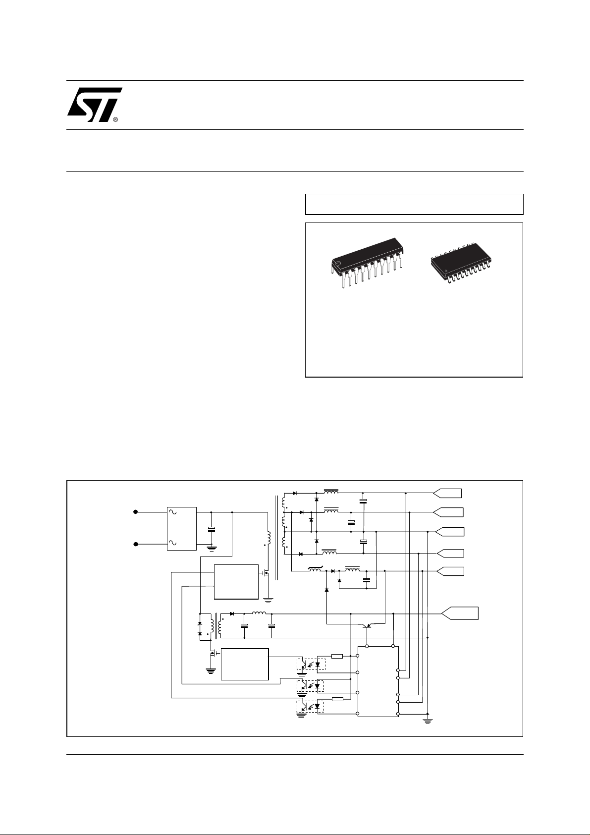
TYPICAL APPLICATION CIRCUIT
+
WIDE RANGE
MAINS
-
April 2002
MAIN
CONTROL
AUXILIARY
CONTROL
Bout
VDD
Cout
MFault
Aout
L6611
Dmon
12V
5V
-12V
3V3
Gnd
+12V
+5V
COM
-12V
+3.3V
+5Vaux
1/28
2/28
L6611
Prog
Dmon
Cinv
Cout
Vdd
Gnd
Ainv
Aout
Bout
Binv
BLOCK DIAGRAM
Vdd
2.50V(B)
uv
ov
ov
OCP Bounce
1.25V (A)
Vdd
L
V
U
V
1.25V (B)
f
V
r
e
Reset
2.50V(A)
2.50V(B)
2.50V(C)
1.25V(A)
1.25V(B)
+5V +12V
2.50V(A)
Soft Start
Logic and Programmable Trimming
2.50V(B)
Programmi ng input
Debounce
75ms
10mA
+
+
_
_
2.50V(C)
Disable
OV
ov
uv
UV
+/-12V UV
ov
uvuvov
3V3 +5V UV
ov
uv
Dfault
Vdd
+12V
+12V
+5V
+5V
Vdd
Vreg
PS-ON / Clock
-
PW-OK / Data
-
50uA
Mfault
ACsns
-
-12V
2.50V(B)
+3V3
+3V3
L6611
DESCRIPTION
The L6611 is a control and housekeeping IC developed in BCD technology; it is intended for acting at the secondary side of desktop PC's or server's switching power supplies, in presence of standard voltage rails (+3.3V,
+5V, ±12V) generated by a main conve rter and of a supply line gen erated by an auxi liar y c onverter. The typic al
application circuit is showed on the front page.
The Housekeeping's main function is to control and monitor the voltages generated by both the main and the
auxiliary converter: it senses those voltages, sends feedback signals to the primary controllers for regulation
and, upon detection of an undervoltage (UV), or overvoltage (OV) condition, reports such fault and takes proper
action to protect the system.
However, the peculiar feature of this IC is its digital programming capability that enables an accurate trimming
of the output voltage rails during product ion test via soft ware, without any use of ex ternal dis crete trimming components or need for manual intervention on the PSU. It is also possible to program some of the monitoring functions and select how UV and OC conditions are handled in the main converter: whether latched-mode (the
information is latched and released only by forcing the restart of the IC) or bouncing-mode (an attempt is made
to automatically restart the converter after 1 second wait).
A key feature of this IC is its contribution to a very low external component count. Besides the extensive use of
onboard programmable switches, which prevents the need for external trimming components, the IC embeds
reference voltages, error amplifiers and most of the housekeeping circuitry normally required.
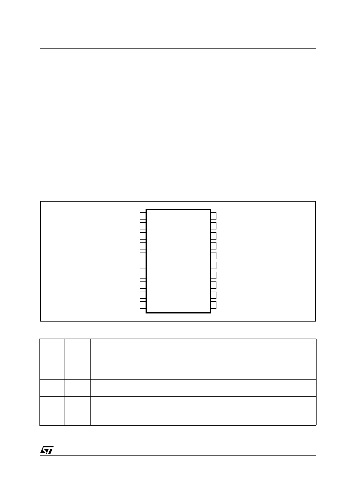
PIN CONNECTION
PIN DESCRIPTION
Pin # Name Description
MFAULT
1
(top view)
MFAULT
MFAULT
Binv
Binv
Bout
Bout
Aout
Aout
Ainv
Ainv
Cout
Cout
Cinv
Cinv
Dmon
Dmon
DFAULT
DFAULT
Vdd
Vdd
Main converter on/off control. This pin is a 10mA current sink used for driving an opto-isolator. It
is normall y low when PS-O N (#13) is p ulled low. If a fault is detected or PS-ON goes high, this
pin goes high too. To allow power up, the functions are digitally blanked out for a period (U VB
function) and MFAULT (#1) stays low. There is no delay for the OV protection function.
12V
12V
5V
5V
3V3
3V3
PROG
PROG
GND
GND
-12V
-
-12V
VREF
VREF
PS-ON
-
PS-ON
-
PW-OK
PW-OK
ACsns
ACsns
2
3
Binv
Bout
Inverting input to the error am plifier for the 3V3 po st-regulator (either m ag-amp or line ar). The
non-inverting input is connected to an internal 1.25V reference that can be digitally trimmed.
Output of the 3V3 error amplifier. It typically drives either a PNP transistor that sets the mag-amp
core or the pass elem ent of a linear re gulator. Also node for error amplif ier compe nsation. T he
maximum positive level of this output is clam ped a t abou t 3.5V to improve response time. La rge
signal slew rate is limited to reduce noise sensitivity.
3/28
L6611
g
y
g
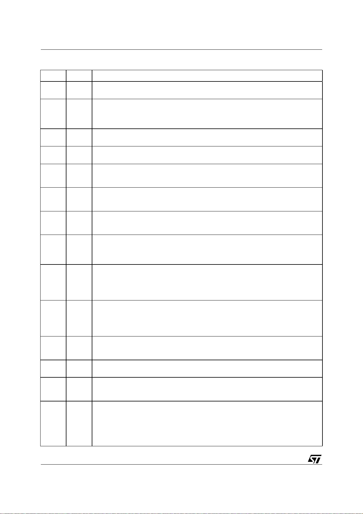
PIN DESCRIPTION
Pin # Name Description
4
5
6
7
8
9
10
11
Aout
Ainv
Cout
Cinv
Dmon
DFAULT
Vdd
ACsns
(continued)
Output of the error amplifier for the main converter. This pin typically drives an optocoupler and is
also used for compensation along with Ainv (pin #5).
Main loop error amplifier inverting input. The non-inverting input is connected to an internal 2.5V
reference that can be digitally trimm ed. A high impe dance inter nal divider from +12V and +5V
UV/OV sense pins (#19, #20 ) eliminates t he need for external d ivider in mos t applicatio ns. The
pin is used for error amplifier compensation.
Auxiliary loop optocoupler drive. Also node for error amp compensation. Large signal slew rate is
limited to reduce sensitivity to switching noise.
Inverting input for Auxiliar y error amplifier. The non-inver ting input is con nected to an inter nal
1.25V reference that can be digitally trimmed.
Dual or Auxiliary UV/OV monitor, Dmon is programmable to monitor 3V3 or 5V . To allow a correct
power up, the UV function on this pin is blanked out dur ing initial star t-u p. There is no delay for
the OV function.
Dual or Auxiliar y fault protection. When Dmon (#8) recognizes an over voltage, DFAULT a nd
MFAULT (#1) go high . DFAULT is capable of sourcing up to 50 mA. Possible applications are a
crowbar across the Auxiliary output or an opto-coupled fault signal to the primary side.
Positive input supply voltage. Vdd is normally sup plied from the Auxiliary power supply output
voltage. If Vdd-UVL detects a sustained under voltage, PW-OK (#12) will be pulled low and
sending MFAULT (#1) high will disable the main converter.
of bulk voltage for AC fail warning. The usual sourc e of this analog pin is one of the
Analo
secondar
current sink on this pin that is activated as the volta
(2.5V).
windings of the main trans former. Hysteresis is prov ided through a trimmable 50µA
e at the pin falls below the internal reference
12
13
14
15
16
17
PW-OK
/Data
PS-ON /
Clock
VREF
-12V
GND
PROG
Power good signal for the Main converter. When asserted high, this pin indicates that the
voltages monitored are above their UV limits. There will be typic ally 2 50m s de lay from th e M ain
outputs becom ing good an d PW-OK being ass er ted. This is nominally a n open drain s ignal. To
improve robustness, this output h as a l imited cu rrent sin k ca pabil ity. In programming mode, this
pin is used for data input; then the absolute maximum rating will be Vdd+0.5V.
Control pin to enable the Main converter. This pin has debouncing logic. A recognized high value
on this pin will cause PW-OK (#12) to g o immediately low a nd, after a delay of 2.5 ms, to shut
down the main PWM by allowing MFAULT (#1) to go high. Durin g norma l operation (or if not
used) this pin has to be connect ed to a voltage lower than 0.8V. In pr ogramming mode, this pin
will be used to clock serial data into the chip.
2.5V reference for external applications. This is a buffered pin. Shor ting this pin to ground or to
Vdd (#10) will not affect integrity of con trol or monitor references. An external capacitor (max.
100nF) is required whenever the pin is loaded (up to 5 mA), otherwise it can be left floating.
-12V UV/OV monitor. If connected to a voltage greater than 1.5V (e.g. VR EF, #14), the funct ion
will be disabled.
Ground pin. The conne ction integrity of this pin is cons tantly monitored and in case of either a
bond wire or a PCB trace going open, MFAULT (#1) and DFAULT (#9) will be forced high
switching off the supply.
The chip has 2 operating modes, depending on PROG input pin biasing:
normal mod
–
programming mod
–
(#12) and PS_ON (#13) pins are disconnected from their normal functionality and they become
inputs for DATA and CLOCK allowing the chip to be programmed. The programming mode allows selecting some options and adjusting some setpoints;
e: PROG should be floating or shorted to ground;
e: forcing PR OG high (+ 5V), the chi p enters pro gramming m ode. PW_ OK
4/28

L6611
PIN DESCRIPTION
Pin # Name Description
18
19
20
3V3
12V
5V
(continued)
3V3 UV/OV monitor. It uses a separate reference to the feedback reference.
Input pin for 5V feedback, 5V current sense and 5V UV/OV monitor. 5V UV/OV uses a reference
separate from t hat used for feedback. This pin conn ects the 5V par t of the Main error amplifier
feedback divider.
Input pin for 12V feedback, 12V current sense and 12V UV/OV monitor.12V UV/OV uses a
reference separate from that used for feedback. This pin connects the 12V part of the Main error
amplifier feedback divider.
FUNCTION DESCRIPTION
Name Description
OVP
UVP
UVB
Whenever one of the Main output voltage s is detected go ing above its own OVP threshold, this
function set MFAULT (#1) high latching the outputs off. The latch is released after cycling PS-ON
(#13) switch or by reducing Vdd (#10) below the UV threshold.
Whenever one of the Main output voltages is detected going und er its own UVP threshold, this
function sets M FAULT (#1) high; if latc h mode has been selected, this fu nction will be latch ed.
Otherwise an attempt wi ll be made to restar t the device after 1 se cond delay. If ACsns (#11) is
low due to a brownout condition, UVP is disabled.
Undervoltage blanking. When either converter is enabled, the relevant UV/OC monitoring circuits
must not intervene to allow all outputs to come within tolerance. 64 ms timing is provided; for the
auxiliar y converter the timin g star ts as the IC has a valid supply, for the main converter it star ts
as the ACsns pin detects a valid input voltage for the converter.
PW-OK delay
OFF delay
Debounce
AC-hysteresis
Vdd-OVP
Vdd-UVL
Dual-OVP
Dual-UVP
PW-OK delay. After power-up, when the all of the monito red voltages are above their own UV
threshold th e PW-OK pin (# 12) will b e kept low for addit ional 250 ms (typ.) to ma ke sure all the
outputs are settled.
Power-off delay. As soon as PS-ON (#13) pin is recognized high, indicating an imminent turn-off
condition, PW-OK (#12) p in will go low immediately . The conver ter will be turned off after a
delay of 2.5ms.
The PS-ON signa l inp ut has d ebou nce logic to prevent improper acti vation. All of the m onito red
inputs have digital filtering/debounce logic on board for high noise immunity.
AC sense hysteresis. Programmable hysteresis is provided on the ACsns input (#11) to avoid
undesired s hutdown caused by noise as the voltage a t the pin is near the threshold or by the
voltage ripple across the bulk capacitor.
Vdd is moni tored for overvoltage. If a n overvoltage is detected, MFAULT (#1) and DFAULT (#9)
are latched high.
To prevent false signals of any of IC’s output pins, an under voltage lock-out circuit monitors Vdd
and keeps all IC’s output at their default OFF level until Vdd reaches a sufficient minimum
voltage for ensuring int egrit y. When Vdd goes be low th e UV th resho ld, all la tches ar e re set and
volatile programming memory cleared.
Dmon (#8) is monitored to detect an overvoltage condition; in this case MFAULT (#1) and
DFAULT (#9) are latched high.
Dmon (#8) is monitored to detect an undervoltage condition; in this case MFAULT (#1) is latched
high and Cout (#6) is pulled low.
5/28
L6611
FUNCTION DESCRIPTION
(continued)
Name Description
The IC provides an on -board 8ms soft-star t, a qua si-monoton ic ramp from 0V to 2.5V for the A
error amplifie r reference voltage, in order to avoid high current peak s in the pr imar y circuit and
Soft-start
output voltage overshoots at star t -up. In fact, if this reference gets the nominal value as soon as
the power-up occurs, the A E/A will go out of regulation and tend to sink much more current, thus
forcing PWM to work with the maximum duty-cycle.
Bounce or
Latch-mode
This option allows setting either latch ed-mode or auto restart after 1 second delay in case of
undervoltage faults.
ABSOLUTE MAXIMUM RATINGS
Symbol Parameter Value Unit
Vdd Supply voltage -0.5 to +7 V
Voltage on PROG, PS-ON/Clock, DFAULT, VREF, and error
amplifier pins
Voltage on MFAULT, PW-OK, Dmon and positive UV, OV, OC, AC
sense pins.
Voltage on and -12V UV/OV sense pin -16 to +5 V
Maximum current in ESD clamp diodes 10 mA
-0.5 to Vdd+0.5 V
-0.5 to +16 V
Operating Junction Temperature -25 to 150 °C
J
Storage Temperature -50 to 150 °C
Lead Temperature (solde ri ng, 10 seconds) 300 °C
L
T
T
STO
T
THERMAL DATA
Symbol Parameter DIP20 SO20 Unit
R
th j-amb
(*) mounted on board
Max. Thermal Resistance junction-to-ambient (*) 70 120 °C/W
6/28
L6611
ELECTRICAL CHARACTERISTCS
(unless otherwise specified: TJ = 0 to 105°C; VDD = 5V, V
V
= VDD, PS-ON = low)
Dmon
Symbol Parameter Test Condition Min. Typ. Max. Unit
SUPPLY SECTION
= 3.3V, V5V = 5V, V
3V3
-12V
= -12V, ,
V
DD(ON)
V
DD(OFF)
Start-up threshold 4.2 4.3 4.6 V
Minimum operating voltage after
3.7 3.8 4.1 V
turn-on
V
DD(H)
V
DDOV
I
DD-ON
Hysteresis 0.25 0.5 0.75 V
Vdd overvoltage 6.1 6.3 6.8 V
Operating supply current No Fault 5 7 mA
FAULT THRESHOLDS
Vout = 3.3V
UV 3V3 undervoltage 2.80 2.90 3.00 V
OV 3V3 overvoltage 4.00 4.15 4.30 V
3V3 bias current 50 65 µ
Vout = 12V
UV 12V undervoltage 10.60 10.80 11.00 V
OV 12V overvoltage 13.50 14.00 14.50 V
12V bias current 100 130 µ
Vout = -12V
A
A
UV -12V undervoltage -9.00 -9.50 -10.0 V
OV -12V overvoltage -14.4 -15.0 -15.6 V
V
-12V disable voltage Voltage to disable comparator 1.3 1.5 1.7 V
D
-12V bias current -65 -50 µ
Vout = 3.3V Aux/Dual (Dmon option)
UV 3V3 undervoltage 2.80 2.90 3.00 V
OV 3V3 overvoltage 4.00 4.15 4.30 V
Vout = 5V Aux/Dual (Dmon option)
UV 5V undervoltage 4.25 4.40 4.55 V
OV 5V overvoltage 6.00 6.25 6.50 V
Bias current 50 65 µ
ACsense / Hysteresis
Bias current V
= 2.7V 5 10 µ
ACsns
A
A
A
7/28
L6611
ELECTRICAL CHARACTERISTCS
(unless otherwise specified: TJ = 0 to 105°C; VDD = 5V, V
V
= VDD, PS-ON = low)
Dmon
(continued)
= 3.3V, V5V = 5V, V
3V3
-12V
= -12V, ,
Symbol Parameter Test Condition Min. Typ. Max. Unit
UV AC undervoltage 2.375 2.50 2.625 V
Trim range -5 +5 %
Trim resolution 0.64 %
I
ACH
Hysteresis current 20 50 80 µ
Hysteresis trim range -20 +20 %
H
Hysteresis adjust step 5 %
S
FAULT OUTPUTS
V
V
MF
POKH
POKL
PW-OK high state No faults 3 V
PW-OK low state I
MFAULT high state leakage PS-ON = high 1 µ
I
L
MFAULT sink current PS-ON = low, V
ISNK
MFAULT OV debounce Minimum OV pulse before
= 15mA 0.4 V
SINK
= 4V 6 10 15 mA
MFAULT
468µ
MFAULT is latched.
A
A
s
DF
D
IOH
FVOH
MFAULT debounce
±12V UV
MFAULT debounce
+5V, 3V3, UV
DFAULT output high source
current
DFAULT output high voltage
Minimum UV pulse before
MFAULT is latched.
Minimum UV pulse before
MFAULT is latched.
Overvoltage condition
DFAULT
= 1.5V
= 0mA, T
amb
= 25oC,
V
I
DFAULT
468µ
250 450 650 µ
-25 -50 -95 mA
2.1 2.4 2.7 V
Overvoltage condition
V
DFAULT output low voltage I
OUT
= 1mA, no faults 0.3 0.5 0.7 V
DFAULT
DFAULT OV debounce Minimum OV pulse before
468µ
DFAULT is latched.
DFAULT UV debounce Minimum UV pulse before
250 450 650 µ
DFAULT is latched.
START-UP / SHUTDOWN FUNCTIONS
t5 DFAULT UV blanking delay Delay from V
(on) to DFAULT
DD
44 64 84 ms
UV active.
t1 MFAULT UV blanking delay Delay from AC
high to Main
SNS
44 64 84 ms
UV active
t2 PW-OK blanking delay Main’s UV good to PW-OK high 175 250 325 ms
s
s
s
s
(t
8/28
t4
DELAY
PS-ON delay time Delay from PS-ON input to
)
MFAULT
1.75 2.5 3.25 ms
L6611
ELECTRICAL CHARACTERISTCS
(unless otherwise specified: TJ = 0 to 105°C; VDD = 5V, V
V
= VDD, PS-ON = low)
Dmon
(continued)
= 3.3V, V5V = 5V, V
3V3
-12V
= -12V, ,
Symbol Parameter Test Condition Min. Typ. Max. Unit
V
V
PS-ON Input High Voltage
IH
PS-ON Input Low Voltage 0.8 V
IL
PS-ON Input high clamp I
= -200µA
I
IN
= 100 µA Vdd
PS-ON
2.0 V
+0.7
R
PS-ON
PS-ON Pull-up to V
DD
t3 PS-ON debounce PS-ON input minimum pulse
V
= 0V 25 50 100
PS-ON
50 75 100 ms
width for a valid logic change.
t
Error Amp. A Soft-Start period VFB quasi-monothonic ramp from
SS
8ms
0 to 2.5V
V
STEP
Soft Start Step Ramp 0V to 2.5V 39 mV
VOLTAGE REFERENCE (BUFFERED EXTERNAL PIN)
V
REF
I
SC
Output Voltage I
Short circuit current V
= 1 - 5 mA; C
REF
= 0 10 20 mA
REF
= 47nF 2.375 2.50 2.625 V
REF
MAIN CONVERTER FEEDBACK (ERROR AMPLIFIER A)
V
Ω
K
V
Input Voltage Tj = 25° C 2.375 2.50 2.625 V
FB
Trim Range About nominal -5 +5 %
Trim resolution 0.64 %
Z
Divider impedance from Ainv to GND. 5V and 12V
FB
35 50 65
connected to GND.
Temperature coefficient 26 Ω/°
W
A
Divider 5/12 weighting 5V contribution to 5/12 feedback 47 50 53 %
5
Voltage gain 2V<V
VOL
<4V 65 dB
OUT
GBW Unity gain bandwidth 3 MHz
PSRR Power supply rejection ratio 4.5V<V
I
OUTL
I
OUTH
V
OUTH
V
OUTL
Output sink current V
Output source current V
Output high level V
Output low level V
FB
FB
FB
FB
<6V 60 70 dB
DD
= 2.7V, V
= 2.3V, V
= 2.3V, I
= 2.7V, I
= 1.1V 2 5 8 mA
OUT
= 4V -1.0 -1.5 -2.0 mA
OUT
SOURCE
SINK
= 1 mA 4 4.5 V
= 2 mA 0.7 1.1 V
MAGAMP OR LINEAR POST-REGULATOR FEEDBACK (ERROR AMPLIFIER B)
V
Input Voltage Tj = 25° C 1.22 1.25 1.28 V
FB
Ω
k
C
Trim Range About nominal -5 +5 %
9/28
 Loading...