

L6605
SMART CARD INTERFACE
ADVANCE DATA
8 DIFFERENTVPP OUTPUTVOLTAGE
LEVELS
V
PP,VCS
RISE AND FALL TIME FULL SPEC
WITHISO/IEC 7816-3
POWER SUPPLY OUTPUT FOR MEMORY
CARD(5V/80mA)
POWER ON/OFF RESET
AUTOMATICSWITCH-OF FOF ALL FUNCTIONS
IF THE REGULAR OPERATION IS ABORTED
BY EXTRACTING THE SMARTCARD
INTERNAL STATUS FAILURE CODING
- INSERTIONFAILURECODE
- OVERTEMPERATUREFAILURE
ANTI-BOUNCINGSYSTEM
INPUT/OUTPUTLOGIC TTL COMPATIBLE
THERMAL PROTECTION
DESCRIPTION
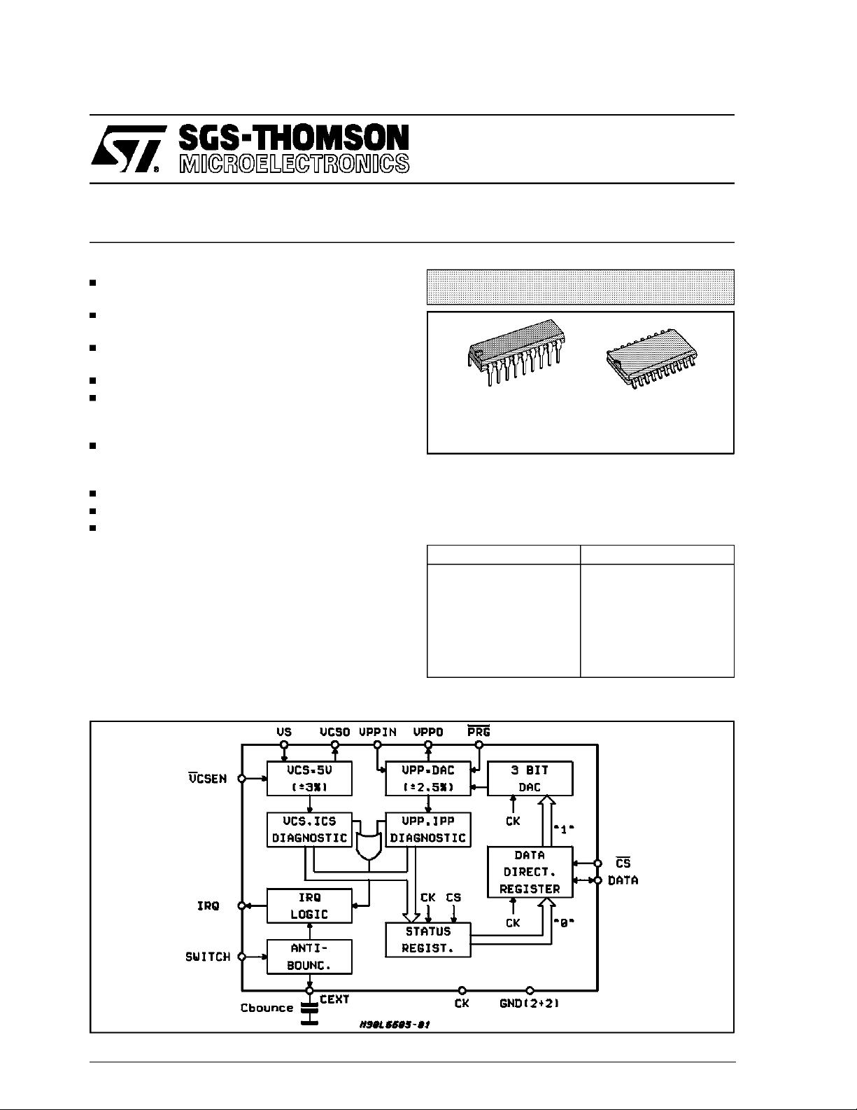
The L6605 is an IC dedicated as intelligent interface between different types of smart cards and
microprocessors. The internal architecture can be
shared in a power supply section and in a diagnosticparts.
The power supply section can deliver5V/80mA to
MULTIPOWERBCD TECHNOLOGY
Powerdip 12+3+3 SO 12+4+4
ORDERING NUMBERS:
L6605 L6605D
supply the card and V
ory inside the card; the V
grammed by means of the 3 serial input bit (see
TAB,1).
Table 1: 3 bit DAC CODE
CODE V
000
001
010
011
100
101
110
111
/50mA to write the mem-
PP
voltage can be pro-
PP
PP
5V
10V
12.5V
13.5V
15V
18V
21V
25V
BLOCK DIAGRAM
December 1992
This isadvanced information on anew product now in development or undergoing evaluation. Details are subject to change without notice.
1/10
L6605
DESCRIPTION (continued)
The diagnostic part allows to monitor failures due
to overtemperature or wrong card positioning.
The failures are internallycoded and readable in-
tional pin DATA configuratedin output.
The antibouncing circuitry, active during card insertion only, rejects ripetitive switching-on of the
powersupply sections.
side the STATUS REGISTERthrough the bidirec-
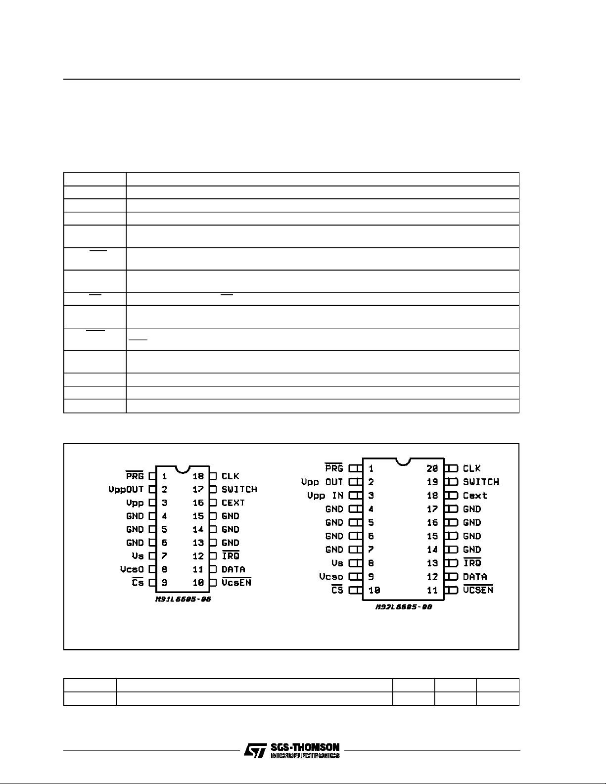
PIN FUNCTION
Pin Description
V
S
V
CSO
V
PPIN
V
PPOUT
V
CSEN
SWITCH Input signal produced by the reader system indicating that a card has been inserted. Internally, an
CS Chip select (active low). CS low level indicates an I/O operationrequest fromµP.
IRQ InterruptRequest (Activelow).
PRG Program (Active low).
DATA I/O pin for data exchange between µP and the device. Through this pin flow 3 bit input DAC or 2 bit
CK External clock.
C
EXT
GND 4 pins to ground.
InputPower Supply voltage for VCSregulated output and for device supply.
Output regulated voltage for card supply; I
= 80mA; overload protected (81to 200mA)
CSmax
Inputpower supply for VPPregulatedvoltage
Programmable output regulated voltage for memory card writing; 8 voltage levels are allowed by
means of 3bit DAC. I
PPmax
= 50mA.
(Active Low) VCS supply input enable; Its value is fixed from the µP allowing or not the normal R/W
operations on the card.
antibouncing system isprovided to avoidmultiple switching.
An IRQ low level indicates that a card insertion/extraction or Failure has occured.
PRG low levelenables L6605 to deliver in output the V
level set by 3 bit DAC.
PPO
STATUS REGISTER code.
Pin to connect an external capacitor for antibouncing delay time.
PIN CONNECTIONS (Top view)
Powerdip 12+3+3 SO 12+4+4
THERMAL DATA
Symbol Parameter L6605 L6605D Unit
R
th j-amb
(*) Soldered ana 35µ thick 6cm2P.C. board copperarea.
Thermal Resistance Junction to Ambient 60 50 (*) °C/W
2/10
L6605
ELECTRICALCHARACTERISTICS (V
= 12V;Tj=25°C)
S
Symbol Parameter Test Condition Min. Typ. Max. Unit
V
S
V
CS
Supply Voltage 10 12 15 V
Card Supply Voltage
ICS= 80mA, VS= 12V
4.85
5
5.15
(Logic Inputsonset)
I
V
I
CS
CSS
PPI
I
= 1mA to 80mA
CS
V
= 10V to 15V
S
C
LOADmin
= 5nF; C
LOADmax
=20µF
Current Supply Card 80 mA
ICSShort Circuit VS = 12V 81 200 mA
VPPSupply Voltage V
4.75
PPO
5
5.25
+
33 V
2.5V
V
PPO
I
PP
I
PPs
t
on
t
off
t
shadow
V
SWLOW
V
SWHIGH
t
CKON
t
CKOFF
t
D
t
SET-UP1
t
HOLD1
t
SET-UP2
t
HOLD2
t
SCK
t
HCK
Programming Voltage IPP= 50mA; V
Output Program. Current V
IPPShort Circuit 51 150 mA
VPP, Rise Time C
VPP, Fall Time 200 µs
Shadow Timing Cbounce = 0.1µF1ms
Low Level Switch Input 0.8 V
High Level Switch Input 2 Vs-2V V
Clock ON Time
Clock OFF Time 1 µs
Delay Time 250 ns
1st bit Set-upTime 500 ns
1st bit Hold Time 500 t
Data Set-up Time 500 ns
Data Hold Time 500 ns
Clock Set-up Time 250 ns
Clock Hold Time 250 ns
= 30V;
T
<5ms
on
= 1mA to 50mA
I
PP
V
= max. 33V (see note 1)
PPI
C
LOAD min
C
LOAD max
= 30V 50 mA
PPI
LOAD min
C
LOAD max
I
= 50mA (see note 1)
L
C
LOAD
V
= 0.4V
L
PPI
= 5nF
= 500nF (see note 2)
= 5nF
= 500nF (see note 2)
= 50pF, I
SINK
= 4mA,
-2.5%
-5%
V
V
DAC
DAC
+2.5%
+5%
200 µs
1 µs
CKON
f Clock Frequency 500 KHz
SR V
Slew Rate From rest state to
PP
2V/µs
programming state and
viceversa
V
STH
V
SHY
T
S
T
H
Note 1: True for values in Tab. 1 only. ; Note 2: Valueshigher than500nF are permitted, but the ton, tofftiming will be out ISO norm.
Power ON/OFF Threshold Logic inputs onset 8.5 9.5 V
V
Hysteresis 0.6 V
STH
Thermal Shutdown 180 °C
Thermal Hysteresis 20 °C
V
V
V
V
ns
CIRCUITOPERATION
CARDPOWER SUPPLY
Regulated voltage to supply the card (5V/80mA).
During nominal condition (V
the V
CS range variationis equal to + 3%.
Whileduring line/load variation(V
I
CS =1mA to 80mA) the VCS range is+ 5%.
An internal circuitry checks the I
S = 12V, ICS = 80mA)
S = 10V to 15V;
CS level; the pro-
tectionblock activates an IRQwith the properfailure code when the output current is in 81mA to
200mA range.
PROGRAMMINGPOWER SUPPLY
L6605 works in step-down mode by means of the
programmed output voltage V
.8VPPlevels can
PP
be selected programming the 3 bit DAC as per
Table 1. During nominal conditions (I
= 30V) the VPPrange variation is equal to
V
PPI
= 50mA;
PP
3/10

L6605
±2.5%; while during line/load variation (IPP= 1mA
to 50mA; V
An internal circuitry checks the I
= max. 33V) the VPPrangeis ±5%.
PPI
level; the pro-
PP
tection block activates an IRQ with the proper failure code when the output current is in 51mA to
150mA range. Under the power ON/OFF threshold value the logic section and the power supply
regulatorsare disabled.
LOGICSECTION
L6605 includes a logic circuitryin order to protect,
both card and itself. If a failure occours an asynchronous IRQ is sent to the µP; consequentlythe
µP forces low CS signal as I/O request. After CS
variation the µP sends also one ”data direction
bit” into DATA DIRECTIONREGISTER.
Directionbit = ”0”
Pin DATA is configuratedin output and the µP
readsthe 2 bitSTATUSREGISTERcontent
Code 1st bit 2nd bit
0 No insertion No Failure
1 Card Inserted Failure
Figure1: Card Insertion
Failurecould be overtemperatureover the 2 regulators(VPP, VCS).
Directionbit = ”1”
Pin DATA is configuratedin input to allow the 3
bit DAC loading and than the programming of
V
outputlevelvoltage.(see Table 1).
PPo
During card insertion only rising edge of switch
signal is detected , while during card extraction
switchlevel is detected.
In card extraction mode if occours a mechanical
switch bouncing, which causes a pulse on
SWITCH input pin with duration t ≥ 50µs the
L6605 will have the 1st Status Register content
equal to ”0” and 1 ms t
timing like during
shadow
cardinsertion mode.
Bouncing on SWITCH pin with duration T<50µs
will be transparent inthe Status Register.
4/10

Figure2: DAC Loadingand ProgrammedVoltage on Set
L6605
5/10

L6605
Figure3: End Normal Operation
6/10

Figure 4.
L6605
Figure5: PAY-TV Application
7/10

L6605
POWERDIP18 PACKAGEMECHANICAL DATA
DIM.
MIN. TYP. MAX. MIN. TYP. MAX.
a1 0.51 0.020
B 0.85 1.40 0.033 0.055
b 0.50 0.020
b1 0.38 0.50 0.015 0.020
D 24.80 0.976
E 8.80 0.346
e 2.54 0.100
e3 20.32 0.800
F 7.10 0.280
I 5.10 0.201
L 3.30 0.130
Z 2.54 0.100
mm inch
8/10

SO20PACKAGE MECHANICAL DATA
L6605
DIM.
MIN. TYP. MAX. MIN. TYP. MAX.
A 2.65 0.104
a1 0.1 0.3 0.004 0.012
a2 2.45 0.096
b 0.35 0.49 0.014 0.019
b1 0.23 0.32 0.009 0.013
C 0.5 0.020
c1 45 (typ.)
D 12.6 13.0 0.496 0.512
E 10 10.65 0.394 0.419
e 1.27 0.050
e3 11.43 0.450
F 7.4 7.6 0.291 0.299
L 0.5 1.27 0.020 0.050
M 0.75 0.030
S 8 (max.)
mm inch
9/10

L6605
Information furnished is believed to be accurate and reliable. However, SGS-THOMSON Microelectronics assumes no responsibility for the
consequences of use of such information nor for any infringement ofpatents or other rights of third parties which may result from its use. No
license is granted by implication or otherwise under any patent or patent rights of SGS-THOMSON Microelectronics. Specifications mentioned in thispublication are subject to change without notice. This publication supersedesand replaces all informationpreviously supplied.
SGS-THOMSON Microelectronics products are not authorized for use as critical components in life support devices or systems without express written approval of SGS-THOMSONMicroelectronics.
1994 SGS-THOMSON Microelectronics - All RightsReserved
SGS-THOMSON Microelectronics GROUP OF COMPANIES
Australia - Brazil- France -Germany -Hong Kong - Italy - Japan- Korea -Malaysia - Malta - Morocco - The Netherlands - Singapore -
Spain - Sweden - Switzerland- Taiwan - Thaliand - United Kingdom - U.S.A.
10/10
 Loading...