

HIGH VOLTAGE RESONANT CONTROLLER
■
HIGH VOLTAGE RAIL UP TO 600V
■
dV/dt IMMUNITY±50V/ns IN FULL
TEMPERATURE RANGE
■
DRIVER CURRENT CAPABILITY:
250mA SOURCE
450mA SINK
■
SWITCHING TIMES 80/40ns RISE/FALL WITH
1nF LOAD
■
CMOS SHUT DOWN INPUT
■
UNDER VOLTAGE LOCK OUT
■
SOFT START FREQUENCY SHIFTING
TIMING
■
SENSE OP AMP FOR CLOSED LOOP
CONTROL OR PROTECTION FEATURES
■ HIGH ACCURACY CURRENT CONTROLLED
OSCILLATOR
■
INTEGRATED BOOTSTRAP DIODE
■
CLAMPING ON Vs
■
SO16, DIP16 PACKAGES
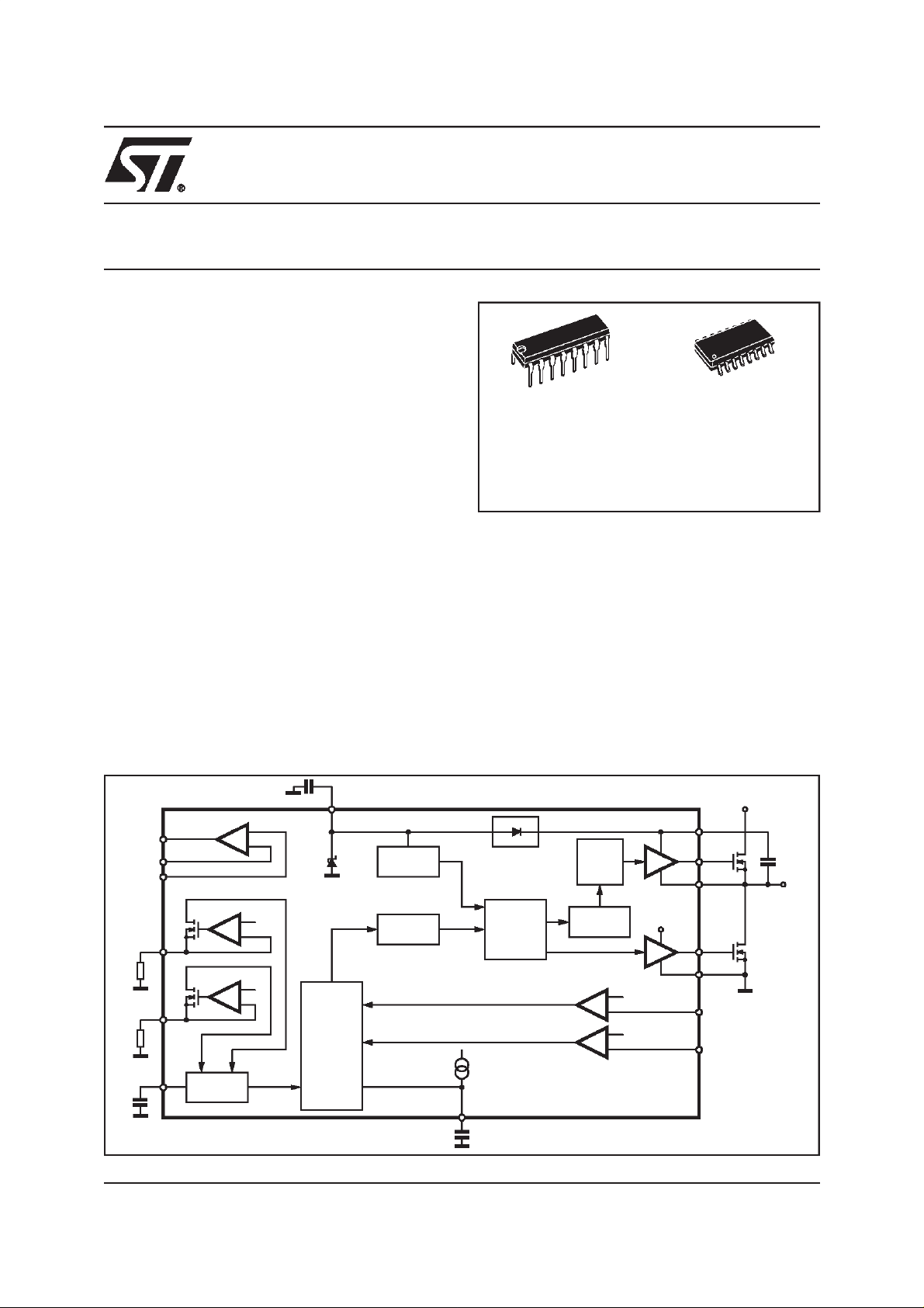
DESCRIPTION
The L6598 is manufactured with the BCD OFF LINE
L6598
DIP16 SO16N
ORDERING NUMBERS:
L6598 L6598D
technology, able to ensure voltage ratings up to
600V, making it perfectly suited for AC/DC Adapters
and wherever a Resonant Topology can be beneficial. The device is intended to drive two Power MOS,
in the classical Half Bridge Topology. A dedicated
Timing Section allows the designer to set Soft Start
Time, Soft Start and Minimum Frequency. An Error
Amplifier, together with the two Enable inputs, are
made available. In addition, the integrated Bootstrap
Diode and the Zener Clamping on low voltage supply, reduces to a minimum the external parts needed
in the applications.
BLOCK DIAGRAM
OP
AMP
5
OPOUT
6
OPIN-
7
OPIN+
Ifmin
4
Rfmin
Rfstart
Cf
February 2000
Ifstart
2
3
VCO
V
S
+
-
V
REF
V
REF
12
CONTROL
LOGIC
UV
DETECTION
DEAD
TIME
Iss
BOOTSTRAP
1
Css
DRIVER
DRIVING
LOGIC
HVG
DRIVER
LEVEL
SHIFTER
LVG DRIVER
+
-
+
-
Vthe1
Vthe2
D98IN887A
16
15
14
Vs
11
10
8
9
V
BOOT
HVG
OUT
LVG
GND
EN1
EN2
H.V.
C
BOOT
LOAD
1/16
L6598
PIN CONNECTION
Css
Rfstart
Cf
Rfmin
OPOUT
OPIN-
OPIN+
1
2
3
4
5
6
7 GND
15
14
13
12
11
10
VBOOT16
HVG
OUT
N.C.
V
S
LVG
EN1 8 EN29
D98IN888
THERMAL DATA
Symbol Parameter SO16N DIP16 Unit
R
th j-amb
Thermal Resistance Junction to Ambient 120 80 °C/W
PIN FUNCTION
N. Name Function
1C
2R
3C
4R
5OP
6OP
7OP
8 EN1 Half Bridge Latched Enable
9 EN2 Half Bridge Unlatched Enable
10 GND Ground
11 LVG Low Side Driver Output
12 V
13 N.C. Not Connected
14 OUT High Side Driver Reference
15 HVG High Side Driver Output
16 V
Soft Start Timing Capacitor
SS
Soft Start Frequency Setting - Low Impedance VoltageSource - See also C
fstart
Oscillator Frequency Setting - see also R
f
Minimum Oscillation Frequency Setting - Low Impedance VoltageSource - See also C
fmin
Sense OP AMP Output - Low Impedance
out
Sense Op Amp Inverting Input - High Impedance
on-
Sense Op Amp Non Inverting Input - High Impedance
on+
Supply Volatge with Internal Zener Clamp
s
Bootstrapped Supply Voltage
boot
fmin,Rfstart
f
f
2/16
ABSOLUTEMAXIMUM RATINGS
Symbol Parameter Value Unit
L6598
I
S
V
LVG
V
OUT
V
HVG
V
BOOT
dV
BOOT/dt
dV
OUT/dt
V
ir
V
ic
V
EN1,VEN2
I
EN1,IEN2
V
opc
V
opd
V
opo
T
stg
Supply Current at Vcl(*) 25 mA
Low Side Output 14.6 V
High Side Reference -1 to V
High Side Output -1 to V
-18 V
BOOT
BOOT
V
Floating Supply Voltage 618 V
VBOOT pin Slew Rate (repetitive) ±50 V/ns
OUT pin Slew Rate (repetitive) ±50 V/ns
Forced Input Voltage (pins Rfmin, Rfstart) -0.3 to 5 V
Forced Input Volatge (pins Css, Cf) -0.3 to 5 V
Enable Input Voltage -0.3 to 5 V
Enable Input Current ±3mA
Sense Op Amp Common Mode Range -0.3 to 5 V
Sense Op Amp Differential Mode Range -5 to5 V
Sense Op Amp Output Voltage (forced) 4.6 V
Storage Temperature -40 to +150 °C
T
T
amb
(*) The device is provided of an internal Clamping Zener between GND and the Vs pin, It must not be supplied by a low impedance voltage
source.
Note : ESD immunity for pins 14, 15 and 16 is guaranteed up to 900 (Human Body Model).
Junction Temperature -40 to +150 °C
j
Ambient Temperature -40 to +125 °C
RECOMMENDED OPERATINGCONDITIONS
Symbol Parameter Value Unit
V
V
out
V
boot
f
max
(*) If the condition Vboot - Vout < 18 is guaranteed, Vout can range from -3 to 580V.
Supply Voltage 10 to V
S
(*) High Side Reference -1 to Vboot-V
(*) Floating Supply Rail 500 V
Maximum Switching Frequency 400 kHz
cl
cl
V
V
3/16
L6598
ELECTRICAL CHARACTERISTCS
(VS=12V;V
BOOT-VOUT
=12V;T
amb
=25°C)
Symbol Pin Parameter Test Condition Min. Typ. Max. Unit
SUPPLYVOLTAGE
V
V
V
suvp
suvn
suvh
12 VSTurnOn Threshold 10 10.7 11.4 V
VSTurnOff Threshold 7.3 8 8.7 V
Supply Voltage Under Voltage
2.7 V
hysteresis
V
cl
I
su
I
q
Supply Voltage Clamping 14.6 15.6 16.6 V
Start Up Current Vs<V
Quiescent Current, fout =
Vs>V
suvn
suvp
2mA
250 µA
60kHz, no load
HIGH VOLTAGESECTION
I
bootleak
I
outleak
R
don
16 BOOT pin Leakage Current V
14 OUT pin Leakage Current V
16 Bootstrap Driver On Resistance 150 Ω
= 580V 5 mA
BOOT
= 562V 5 mA
OUT
HIGH/LOW SIDE DRIVERS
I
hvgso
15 High Side Driver Source Current V
HVG-VOUT
= 0 170 250 mA
I
hvgsi
I
lvgso
I
lvgsi
t
rise
t
fall
15,11 Low/High Side Output Rise Time C
High Side Driver Sink Current V
11 Low Side Driver Source Current V
Low Side Driver Sink Current V
HVG-VBOOT
LVG-GND
LVG - VS
load
C
load
= 0 300 450 mA
= 0 170 250 mA
= 0 300 450 mA
= 1nF 80 120 ns
= 1nF 40 80 ns
OSCILLATOR
DC 14 Output Duty Cycle 48 50 52 %
f
min
Minimum Output Oscillation
Cf= 470pF; R
= 50k 58.2 60 61.8 kHz
fmin
Frequency
f
start
V
ref
Soft Start Output Oscillation
Frequency
2, 4 Voltageto Current Converters
Cf= 470pF; R
=47k
R
fstart
fmin
= 50k;
114 120 126 kHz
22
Threshold
t
d
14 Dead Time between Low and
0.2 0.27 0.35
High Side Conduction
TIMING SECTION
k
ss
1 Soft Start Timing constant Css= 330nF 0.115 0.15 0.185 s/µF
s
µ
4/16
L6598
ELECTRICAL CHARACTERISTCS (continued)
Symbol Pin Parameter Test Condition Min. Typ. Max. Unit
SENSE OP AMP
l
IB
V
R
out
I
out-
I
out+
V
GBW Sense Op Amp Gain Band
G
COMPARATORS
V
the1
V
the2
t
pulse
6, 7 Input Bias Current 0.1 µA
io
ic
dc
Input Offset Voltage -10 10 mV
5 Output Resistance 200 300
Source Output Current V
Sink Output Current V
6,7 OP AMP input common mode
range
Width Product
DC Open Loop Gain 80 dB
8 Enabling Comparator Threshold 0.56 0.6 0.64 V
9 Enabling Comparator Threshold 1.05 1.2 1.35 V
8,9 Minimum Pulse lenght 200 ns
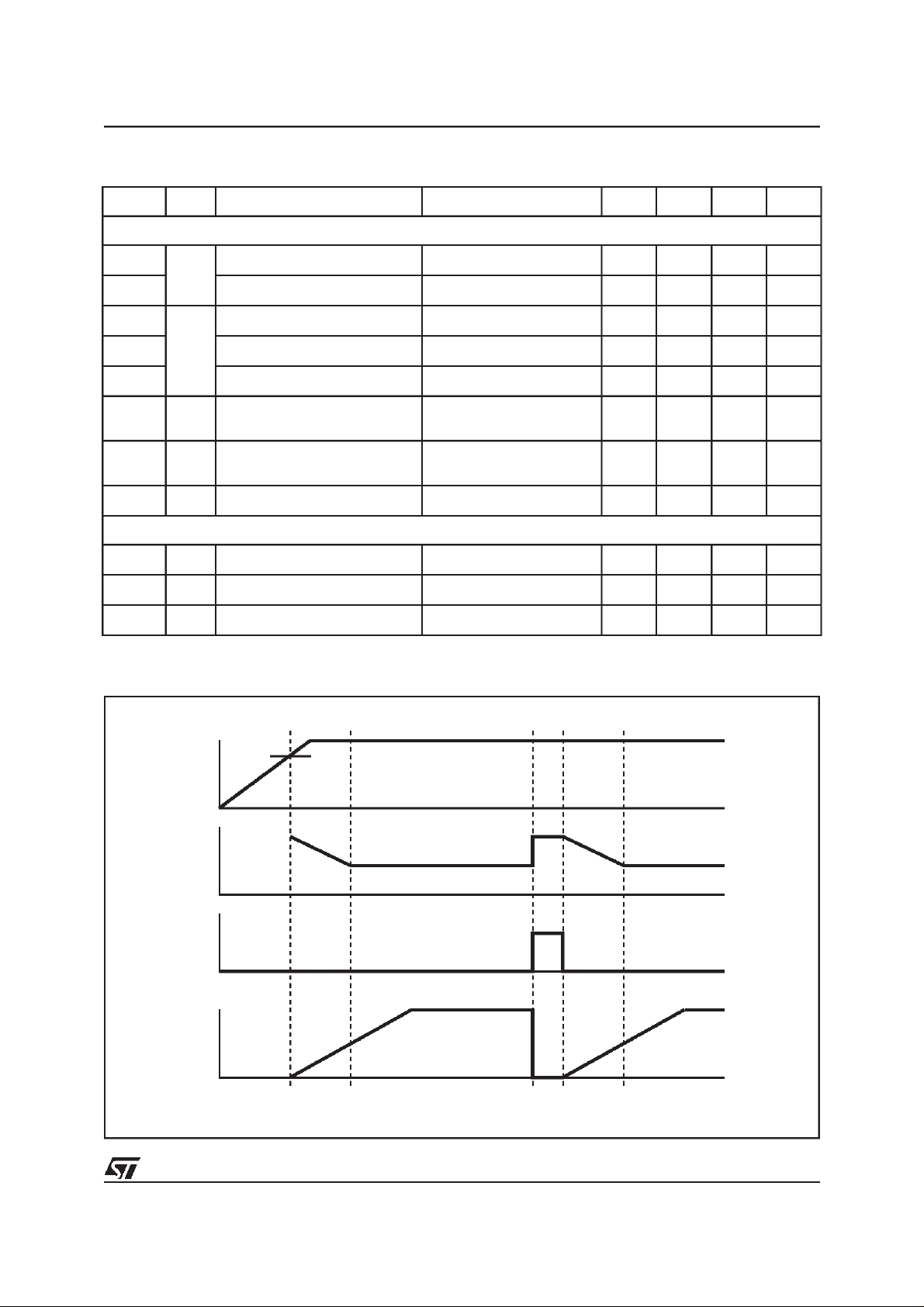
Figure 1. EN2 Timing Diagrams
= 4.5V 1 mA
out
= 0.2V 1 mA
out
-0.2 3 V
1MHz
Ω
V
S
f
OUT
EN2
V
Css
fstart
fmin
T
SS
T
SS
D98IN889
5/16

L6598
Figure 2. EN1 Timing Diagrams
HVG
LVG
EN1
EN2
Figure 3. Oscillator/Output Timing Diagram
D98IN890
C
f
HVG
LVG
D98IN897
High/LowSide drivingsection
An High and Low Side driving Section provide the proper driving to the external Power MOS or IGBT. An high
sink/source driving current (450/250 mA typ)ensure fast switching times also when size4 Power MOS are used.
The internal logic ensures a minimum dead time to avoid cross-conduction of the power devices.
Timingand Oscillator Section
The L6598 isprovided of a soft start function. It consists in a period of time, TSS, in whichthe switching frequen-
to f
cy shifts from f
start
. This feature is explained in the following description (ref. fig.4 and fig.5).
min
6/16

Figure 4. Soft Start and frequency shifting block
L6598
IfminIfstartIss
----------------+
R
1
fsta rt
Iosc
gmI
--------------
C
ss
[3]
ss
[1]
t–
gm OSC
Css
During the softstart time the currentISScharges the capacitor CSS, generating a voltage ramp which is delivered
to a transconductance amplifier, as shown in fig. 4. Thus this voltage signal is converted in a growing current
which issubtracted to I
start is equal to:
I
osc
At the start-up (t=0) the L6598 oscillates at f
. Therefore the current whichdrives the oscillator to set the frequency during the soft
fstart
I
fminIfstartgmVCss
V
REF
I
where [2]
I
osc
fmin
0() I
--------------
R
fmin
start
==
+
fminIfstart
t()–()+ I
,
I
fsart
, set by:
fminIfstart
V
REF
----------------
R
fstart
V
REF
+==
, 2V== =
V
REF
1
--------------
R
fmi n
At the end of soft start (t = T
only by I
Since the second term of eq.1 is equal to zero, we have:
Note that there is not a fixed threshold of the voltage across C
the frequency shifting), and T
the I
SS
In this way the soft start time depends only on the capacitor C
(i.e. R
min
current has been designed to be a fraction of I
I
SS
fmin
):
I
fstart
--------------
) the second term of eq.1 decreases to zero and the switching frequency is set
SS
I
()I
K
oscTss
gmI
ss
-------------- T
– 0T
I
fsta rt
SS
C
depends on CSS,I
TSS→
SS
ss
C
ssIfstart
--------------------------
gmI
fstart
fmin
→
fstart,gm
,so:
fstart
TSS→
K
SS
, and ISS(eq. 5). Making TSSindependent of I
V
REF
--------------==
R
SS
[4]
fmin
C
ssIfstart
------------------------==
gmI
in which the soft start finishes (i.e. the end of
C
ss
-----------
gmK
. The typical value of the kSSconstant (Soft
SS
[5]
ss
T
–→== =
SSkSSCSS
[6]
fstart
7/16
,

L6598
Start Timing Constant) is 0.15 s/µF.
The current I
wave on the oscillator capacitor C
to compute an approximate value of the oscillator frequency in normal operation is:
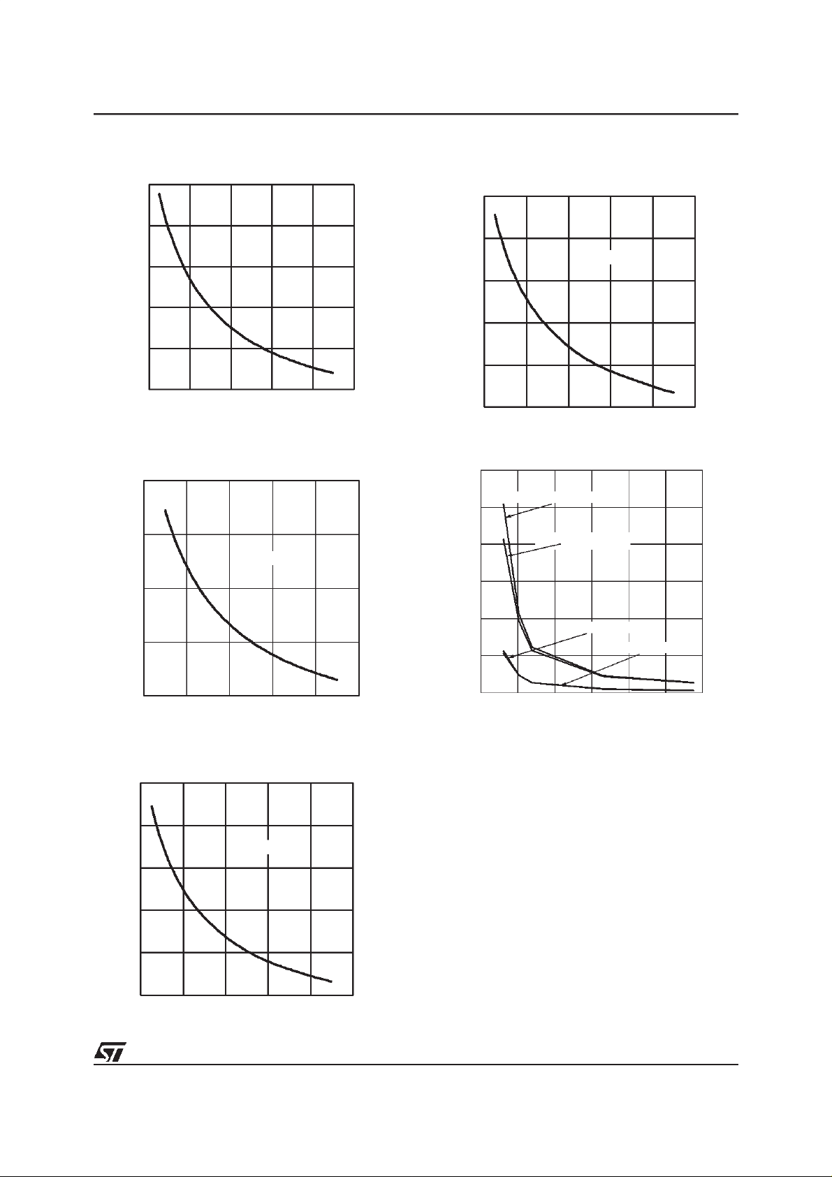
The degree of approximation depends on the frequency value,butit remains very good inthe range from 30kHz
to 100kHz (figg.6-10)
Figure 5. Oscillator Block
is fed to the oscillator asshown infig. 5. It is twice mirrored (x4 and x8) generating the triangular
osc
. Referring to the internal structure of the oscillator (fig.5), a good relationship
f
1.41
f
min
--------------------=
R
fminCf
[7]
X4Iosc
Vth+
Vth-
+
S
R
+
X8
Cf
8/16
L6598
Figure 6. Typ. fmin vs. Rfmin @ Cf = 470pF
f
min
(KHz)
D98IN891
100
80
60
40
20
20 40 60 80 100 R
fmin
(KΩ)
Figure 7. Typ. (fstart-fmin) vs. Rfstar @
Cf = 470pF
∆
f
(KHz)
80
Rfmin=33KΩ
D98IN892
Figure 9. Typ. (fstart-fmin) vs. Rfstar @
Cf = 470pF
∆
f
(KHz)
100
Rfmin=100KΩ
80
60
40
20
20 40 60 80 100 R
D98IN894
fstart
Figure 10. fmin @ different Rf vs Cf
fmin
(KHz)
400
Rf=19.9Kohm - calc.
Rf=19.9Kohm- meas.
(KΩ)
60
40
20
20 40 60 80 100 R
fstart
Figure 8. Typ. (fstart-fmin) vs. Rfstar @
Cf = 470pF
f
∆
(KHz)
100
Rfmin=50KΩ
80
60
40
D98IN893
(KΩ)
200
0
0 200
Rf=90Kohm- meas.
Rf=90Kohm- calc.
400
Cf (pF)
20
20 40 60 80 100 R
fstart
(KΩ)
9/16

L6598
BootstrapSection
The supply of the high voltage section is obtained by means of a bootstrap circuitry. This solution normally requires an high voltage fast recovery diode for charging thebootstrap capacitor (fig. 11a). In the L6568 a patented integrated structure, replaces this external diode. It is realised by means of a high voltage DMOS, driven
synchronously with the low side driver (LVG), with in series a diode, as shown in fig. 11b.
Figure 11. ootstrap driver
BOOT
D
VS VBOOT
CBOOT
VOUT
VS VBOOT
LVG
VOUT
C
BOOT
ab
To drive the synchronised DMOS it is necessary a voltage higher than the supply voltage Vs. This voltage is
obtained by means of an internal charge pump (fig. 11b).
The diode connected in seriesto the DMOS has been added to avoid undesirable turn on of it. The introduction
of the diode prevents any current can flow from the V
turned off when the internal capacitor of the pump is not fully discharged.
The bootstrap driver introduces a voltage drop during the recharging of the capacitor C
side driver is on), which increases with the frequency and withthe size of the external power MOS. It is the sum
of the drop across the R
and of the diode threshold voltage. At low frequency this drop is very small and
DSON
can be neglected. Anyway increasing the frequency it must be taken in to account. In fact the drop, reducing
the amplitude of the driving signal, can significantly increase the R
dissipation).
To be considered that in resonant power supplies the current which flows in the power MOS decreases increasing the switching frequency and generally the increases of R
is negligible. The following equation is useful to compute the drop on the bootstrap driver:
pin to the VSone in case that the supply is quickly
boot
(i.e. when the low
boot
of the external power MOS (and so the
DSON
is not a problem because power dissipation
DSON
Q
g
-------------------
T
ch earg
R
+==
dsonVdiode
[8]
is the on resistance of the bootstrap DMOS, and
where Q
T
charge
V
drop
isthe gate charge of the external power MOS, R
g
I
ch eargRdson
V
diode
V
→+
drop
dson
is the time in which the bootstrap driver remains on (about the semiperiod of the switching frequency
minus the dead time). The typical resistance value of the bootstrap DMOS is 150 Ohm. For example using a
power MOS with a total gate charge of 30nC the drop on the bootstrap driver is about 3V, at a switching frequency of 200kHz. In fact:
30nC
V
drop
------------------ 150Ω 0.6V~2.6V+=
2.23µs
To summarise, ifa significant drop on the bootstrap driver (at high switching frequency when large power MOS
are used) represents a problem, an external diode can be used, avoiding the drop on the R
10/16
DSON
of the DMOS.

L6598
OP AMP Section
The integrated OP AMP is designed to offerLow Output Impedance, wide band,High input Impedance and wide
Common Mode Range. It can be readily used to implement protection features or a closed loop control. For this
purpose the OP AMP Output can be properly connected to R
Comparators
Two CMOS comparators are available to perform protection schemes. Short pulses (>= 200ns) on Comparators
Input are recognised. The EN1 input (active High), has a threshold of 0.6V (typical value) forces the L6598 in a
latched shutdown state (e.g. LVG Low, HVG low,Oscillator stopped), asin the Under Voltage Conditions. Normal Operating conditions are resumed after a power-off power-on sequence. The EN2 input (active high), with
a threshold of 1.2V (typical value) restarts a Soft Start sequence (see Timing Diagrams). In addition the EN2
Comparator, when activated, removes a latched shutdown caused by EN1.
Figure 12. Switching Time Waveform Definitions
pin to adjust the oscillation frequency.
fmin
90% 90%
HVG
90% 90%
LVG
10% 10%
t
r
10% 10%
t
r
t
f
Figure 13. Dead Time and Duty Cycle Waveform Definition
T
1
t
d
50%
HVG
t
50%
t
f
D98IN898
d
T
T
period
1
Dc =
LVG
50%
50%
T
period
50%
D98IN899
11/16
L6598
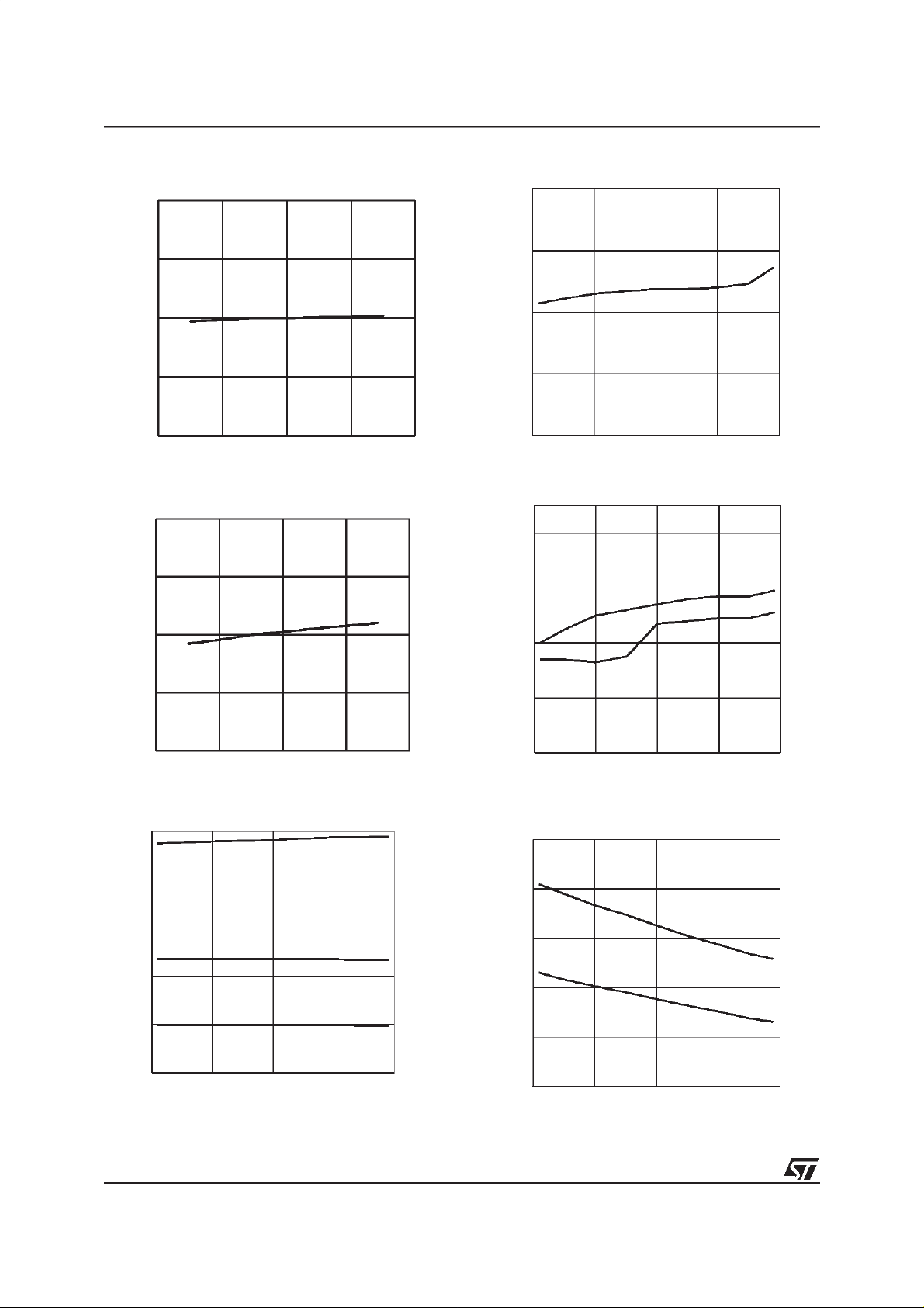
Figure 14. Typ. fmin vs. Temperature
f
min
(KHz)
70
60
50
40
-50 0 50 100
Figure 15. Typ. fstart vs. Temperature
f
fstart
(KHz)
130
D98IN896
D98IN895
T(°C)
Figure 17. Start Up Current vs Temperature
Isu
(µA)
200
150
100
50
-50
050
100
T(°C)
Figure 18. Quiescent Current vs Temperature
Iq
(mA)
2.3
2.1
Iq @Vclamp
120
110
100
-50 0 50 100
T(°C)
Figure 16. Vs thresholds and clamp vs temp.
Vs
(V)
14
12
10
8
6
-50 0 50
100
Vclamp
Vsuvp
Vsuvn
T(°C)
Iq @12V
1.9
1.7
1.5
-50
0
50
100
T(°C)
Figure 19. HVG Source and Sink Current vs.
Temperature
Ihvg
(mA)
500
400
Ihvg sinkcurr.
300
200
100
-50 0 50
Ihvg sourcecurr.
100
T(°C)
12/16
L6598
Figure 20. LVG Source and Sink Current vs.
Temperature
Ilvg
(mA)
500
400
Ilvg sink curr.
300
200
100
-50
0 50 100
Ilvg sourcecurr.
T(°C)
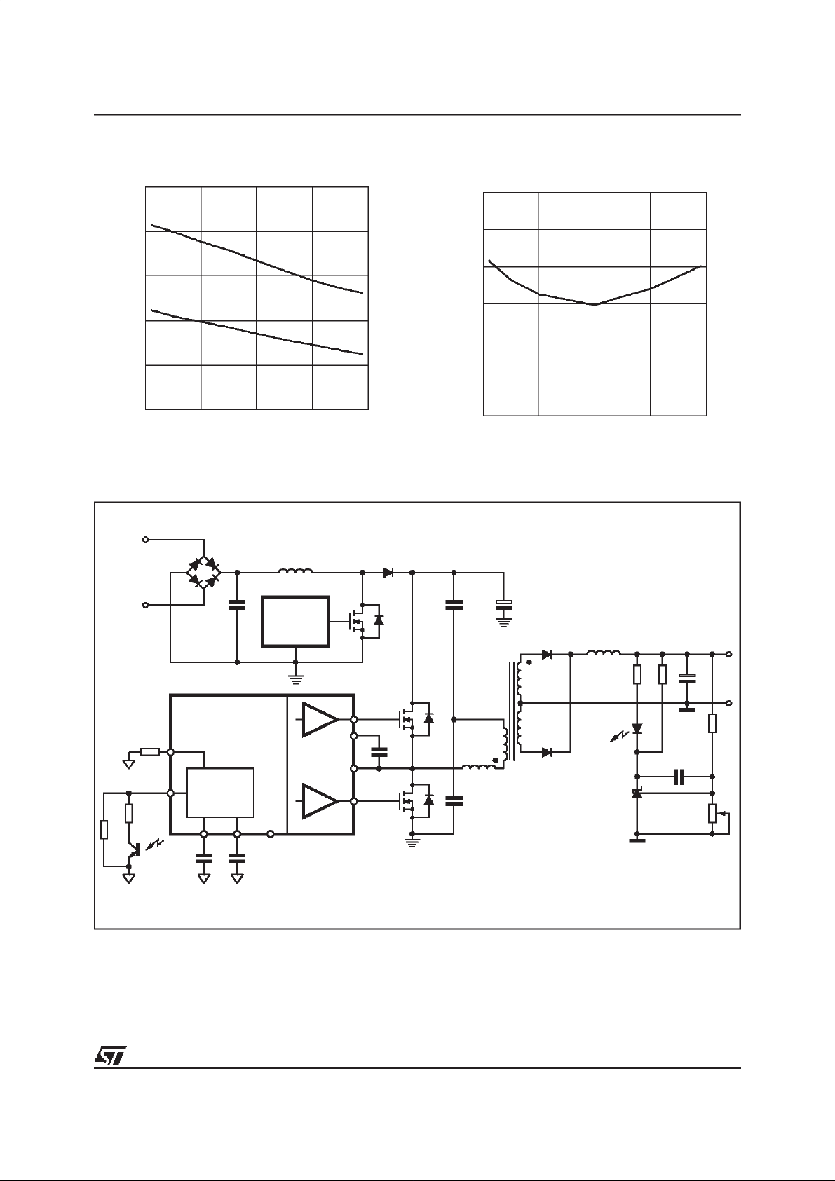
Figure 22. Wide Range AC/DC Adapter Application
Figure 21. Soft Start Timing Constant vs.
Temperature
kss
(s/µF)
0.16
0.14
0.12
-50
0 50 100
T(°C)
85 to
Vac
270
L6598
VCO
&
CONTROL
L6561
Vo
DRIVER
TL431
ENABLE
D98IN874A
13/16
L6598
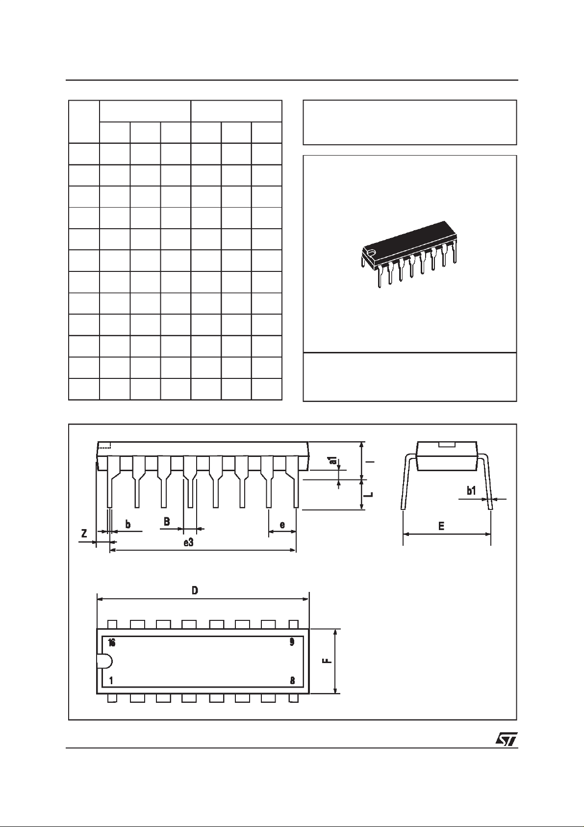
DIM.
MIN. TYP. MAX. MIN. TYP. MAX.
a1 0.51 0.020
B 0.77 1.65 0.030 0.065
b 0.5 0.020
b1 0.25 0.010
D 20 0.787
E 8.5 0.335
e 2.54 0.100
e3 17.78 0.700
F 7.1 0.280
I 5.1 0.201
L 3.3 0.130
Z 1.27 0.050
mm inch
OUTLINE AND
MECHANICAL DATA
DIP16
14/16

L6598
DIM.
MIN. TYP. MAX. MIN. TYP. MAX.
A 1.75 0.069
a1 0.1 0.25 0.004
a2 1.6 0.063
b 0.35 0.46 0.014 0.018
b1 0.19 0.25 0.007 0.010
C 0.5 0.020
c1 45° (typ.)
D (1) 9.8 10 0.386 0.394
E 5.8 6.2 0.228 0.244
e 1.27 0.050
e3 8.89 0.350
F (1) 3.8 4 0.150 0.157
G 4.6 5.3 0.181 0.209
L 0.4 1.27 0.016 0.050
M 0.62 0.024
S
mm inch
0.009
8°(max.)
OUTLINE AND
MECHANICAL DATA
SO16 Narrow
(1) Dand F do not include mold flashor protrusions. Mold flash or potrusions shall not exceed0.15mm (.006inch).
15/16

L6598
Information furnished is believed tobe accurate and reliable. However, STMicroelectronics assumes no responsibility for the consequences
of useof suchinformation nor for any infringement of patents or otherrights ofthird parties whichmayresult fromits use. No license isgranted
by implicationor otherwise under any patent or patent rights of STMicroelectronics. Specifications mentioned in this publication are subject
to change without notice. This publication supersedes and replaces all information previously supplied. STMicroelectronics products are not
authorized for use as critical components in life support devices or systems without express written approval of STMicroelectronics.
The ST logo is a registered trademark of STMicroelectronics
2000 STMicroelectronics - All Rights Reserved
Australia - Brazil -China - Finland - France - Germany - Hong Kong - India - Italy - Japan - Malaysia -Malta- Morocco - Singapore - Spain
STMicroelectronics GROUP OF COMPANIES
- Sweden - Switzerland - UnitedKingdom - U.S.A.
http://www.st.com
16/16
 Loading...