

FULLY INTEGRATED POWER SUPPLY FIPS
Features
WIDE-RANGE MAINS OPERATION
”ON-CHIP” 700V BVDSS POWERMOS
65kHzINTERNAL OSCILLATOR
2.5V ±2%INTERNALREFERENCE
STANDBY MODE FOR HIGH EFFICIENCY
AT LIGHT LOAD
OVERCURRENT AND LATCHED OVERVOL-
TAGE PROTECTION
NON DISSIPATIVE BUILT-INSTART-UP CIR-
CUIT
ON-CHIP SOFT START AND THERMAL
SHUTDOWN
Main Applications
WALLPLUGPOWERSUPPLYUP TO15W
AC-DC ADAPTORS
AUXILIARYPOWER SUPPLY:
- MONITORS (BLUE ANGEL)
- DESKTOPS/SERVERS
- FAX,TV, LASER PRINTERS
- HOME APPLIANCES/LIGHTING
LINECARD, DC-DC CONVERTERS
L6590
PRODUCT PREVIEW
Minidip SO16W
DESCRIPTION
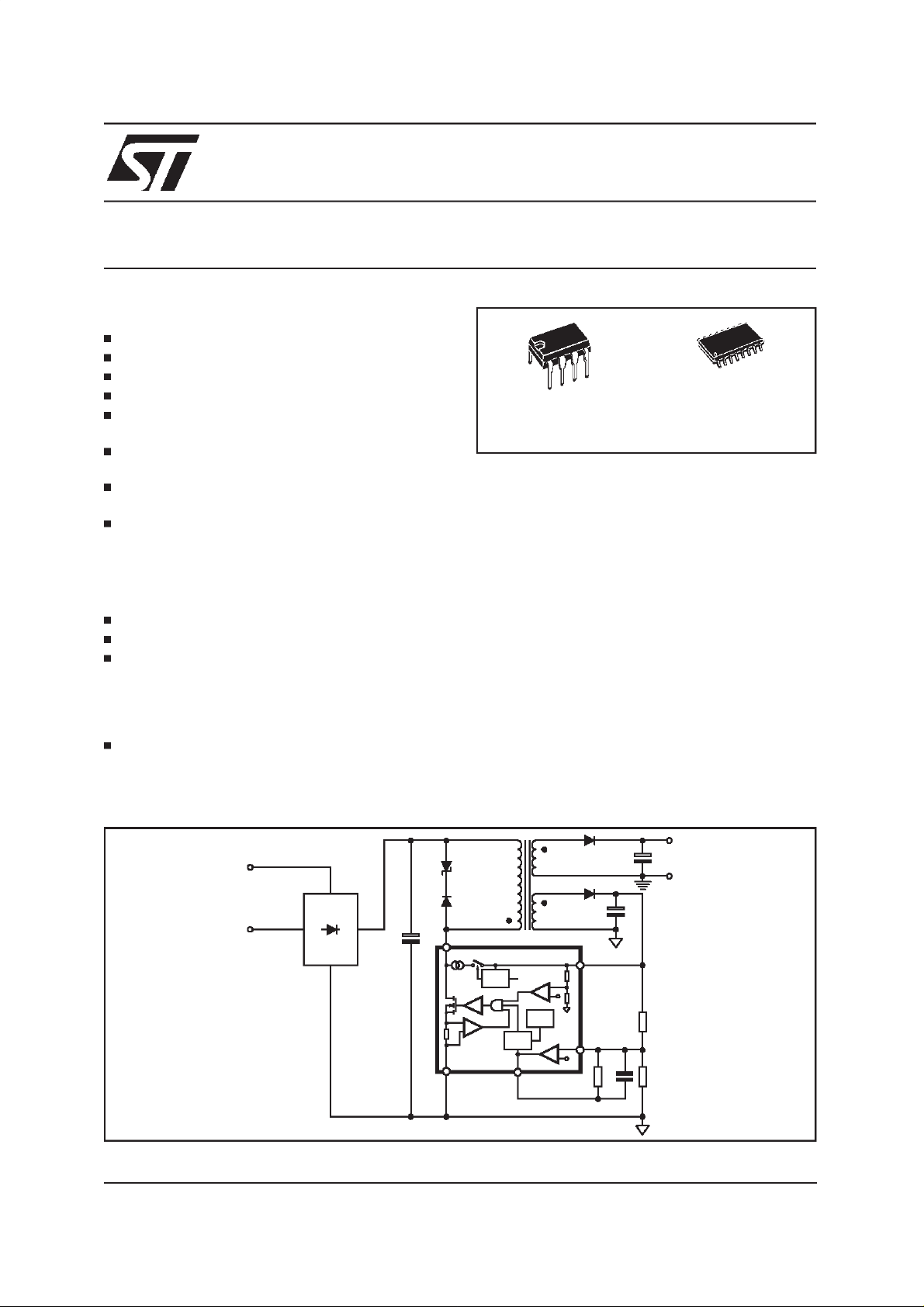
The L6590 is a monolithicswitching regulator designed in BCDOFF-LINE technology,able to operate with wide range input voltage and delivering
an output power up to 13W. The internal switch.
is implemented by a lateral high voltage power
Mosfet with an Rdson of 13Ω and a BVDss of
700V. The internal fixed oscillator frequency, non
dissipative start up and the internal soft start system allow to minimize the components count. A
2.5V+/-2% internalreference in addition to a high
gain error amplifier make the device suitable for
low cost applications with primary control.
Internal protectionslike cycle by cycle current limiting, output overvoltage protection and thermal
shutdowngenerate a ’robust’design solution.
The device automatically reduces the frequency
from 65KHz to 22KHz under light load conditions
improvingthe efficiency.
TYPICALAPPLICATIONCIRCUIT
PO=15W
AC
LINE
85VACto 265V
May 1999
This is preliminary information on a new product now in development. Details are subject to change without notice.
AC
DRAIN
V
V
REF
+
-
CC
VFB
2.5V
D98IN857
+
OVER
CURRENT
L6590
SUPPLY
& UVLO
OVER
VOLTAGE
V
REF
+
-
OSC
100KHz
PWM
VCOMPGND
1/8
L6590
ABSOLUTE MAXIMUM RATINGS
Symbol Parameter Value Unit
V
ds
I
d
V
cc
P
tot
T
j
T
stg
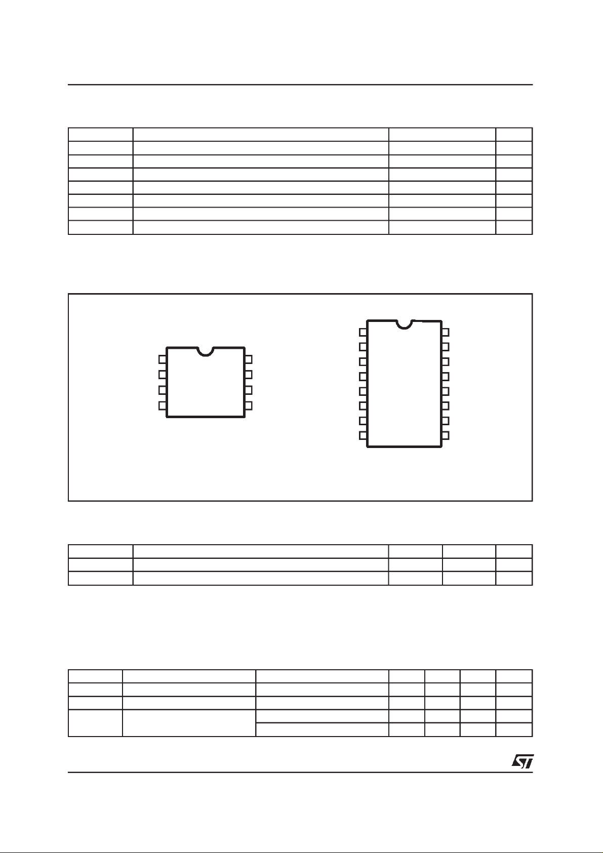
PINS CONNECTION(Top views)
Drain Source Voltage 700 V
Drain Current 0.7 A
Supply Voltage 18 V
Error Amplifier Output Sink Current 3 mA
Power Dissipation at T
<50°C (Minidip) 1 W
amb
Junction Operating Temperature Range -40 to 150 °C
Storage Temperature -40 to 150 °C
DRAIN
N.C.
V
CC
VCOMP
1
2
3
4 VFB
D98IN854A
GND8
GND
7
GND
6
5
DRAIN
N.C.
N.C.
V
CC
SGND
ENABLE
VCOMP
VFB
1
2
3
4
5
6
7 PGND
8 PGND9
D98IN855A
15
14
13
12
11
10
PGND16
PGND
PGND
PGND
PGND
PGND
MINIDIP SO16W
THERMAL DATA
Symbol Parameter Minidip SO16W Unit
R
th j-amb
R
th j-amb
(*) Value depending from PCB copper areas and thikness.
Thermal ResistanceJunction to Ambient Free Air 60 - °C/W
Thermal ResistanceJunction to Ambient (*) 35 to60 35 to 60 °C/W
ELECTRICALCHARACTERISTICS (T
= 0to 105°C,Vcc= 10V)
j
Power Section
Symbol Parameter Test Condition Min. Typ. Max. Unit
Drain Source Voltage Id= 500µA 700 V
Off State Drain Current Vds= 560V 500
Drain Source on state
Resistance
Id= 25mA; Tj = 25°C1317
Tj = 125°C2635
2/8
BV
R
I
dss
dson
dss
A
µ
Ω
Ω
ELECTRICALCHARACTERISTICS (continued)
Symbol Parameter Test Condition Min. Typ. Max. Unit
Error Amp Section
L6590
V
fb
Input Voltage Tj = 25°C 2.45 2.5 2.55 V
Tj = 125°C 2.43 2.5 2.57 V
I
b
Input Bias Current -0.3 -1
Avol 60 dB
B Unity Gain Bandwidth 0.7 1 MHz
SVR Supply Voltage Rejection 70 dB
I
source
V
V
oh
ol
Output Source Current Vcomp = 3.5V 0.5 1 mA
V
High I
out
V
Low I
out
= 0.5mA Vfb= 2V 3.8 4.5 V
source
= 1mA Vfb= 3V 1.0 V
sink
OscillatorSection
F
osc
Dmin Min. Duty Cycle Vcomp = 1V 0 %
Dmax Max. Duty Cycle 66 70 74 %
Oscillator Frequency Tj = 25°C 586572KHz
56 65 74 KHz
Device Operation Section
I
op
I
psc
V
z
V
ddon
V
ddoff
Operating Supply Current 6 8 mA
Peak Start up Current Vcc= 0V 5 10 15 mA
Zener Voltage 17 17.5 18 V
Start Threshold Voltage 14 14.5 15 V
Min Operating Voltage After
7 7.5 8 V
Turn on
Soft Start
V
ccss
Soft Start Threshold Voltage 12 12.5 13 V
Circuit Protections
A
µ
I
lim
Pulse by Pulse Current Limit dI/dt= 0.2A/µs 500 625 700 mA
OVP Over Voltage Protection 15 15.5 16 V
t
m
Internal Masking Time 120 ns
Stand by Section
I
pksb
F
stb
I
pknor
PN/OFF/BROWN-OUT
V
th on
I
Hyst
I
off
I
p
V
CL
THERMAL SHUTDOWN (*)
(*) Parameter not tested in production.
Current Threshold for Stand-By
Operation
Transition from 65KHz to
22KHz
70 mA
Stand by Frequency Tj = 25°C 192327KHz
Current Threshold for Normal
Operation
Stand by current f
Transition from 22KHz to
170 mA
65KHz
= fstand-by 5 7.5 mA
SW
Threshold Voltage (Device on) 2.425 2.5 2.575 V
Source Current V
Supply Current in Off Condition V
Source Current V
On/Off Clamp Pull-Up Voltage I
=3V 305070
pin
= 2V 0.5 mA
pin
=2V 5 mA
pin
= 0.5mA 5 5.5 6 V
sink
Thermal Shutdown 150 165 °C
Hysteresis 40 °C
A
µ
3/8

L6590
APPLICATIONEXAMPLES
Figure 1. AC-DC Adaptor, AuxiliaryP.S. (Isolated bias winding feedback)
AC LINE
85V
to 265V
AC
WIDE RANGE MAINS
FULLY ISOLATED SOLUTION
MINIMUM COMPONENTS COUNT
Figure 2. High Performance AC-DC Converter.(Secondaryreferenced optcouplerfeedback)
AC LINE
to 265V
85V
AC
AC
DRAIN
V
L6590
GND
AC
CC
VFB
COMP
D98IN850
L6590
WIDE RANGE MAINS
FULLY ISOLATED SOLUTION
EXCELLENT OUTPUT PRECI-
SION ANDREGULATION
Figure 3. High Voltage DC-DC Converter.
NOT ISOLATION
MINIMUM PARTS COUNT
EXCELLENT OUTPUT PRECISION
STEP DOWN OR STEP UP TOPOLOGIES
GND
VFB
GND
DRAIN
V
CC
COMP
COMP
L6590
DRAIN
V
CC
VFB
D98IN851
D98IN852
4/8

APPLICATIONEXAMPLE(continued)
Figure 4. Line Card Application. (Isolated bias winding feedback)
0
DRAIN
V
CC
VFB
MINIMUM COMPONENTS COUNT
FULLY ISOLATED SOLUTION
L6590
-48V
GND
COMP
L6590
+5V
-5V
D98IN853
5/8

L6590
DIM.
MIN. TYP. MAX. MIN. TYP. MAX.
A 2.35 2.65 0.093 0.104
A1 0.1 0.3 0.004 0.012
B 0.33 0.51 0.013 0.020
C 0.23 0.32 0.009
D 10.1 10.5 0.398 0.413
E 7.4 7.6 0.291 0.299
e 1.27 0.050
H 10 10.65 0.394 0.419
h 0.25 0.75 0.010 0.030
L 0.4 1.27 0.016 0.050
K0°(min.)8° (max.)
mm inch
0.013
OUTLINE AND
MECHANICAL DATA
SO16 Wide
L
hx
45
A
B
e
K
A1
C
H
D
16
9
E
1
8
6/8

L6590
DIM.
MIN. TYP. MAX. MIN. TYP. MAX.
A 3.32 0.131
a1 0.51 0.020
B 1.15 1.65 0.045 0.065
b 0.356 0.55 0.014 0.022
b1 0.204 0.304 0.008 0.012
D 10.92 0.430
E 7.95 9.75 0.313 0.384
e 2.54 0.100
e3 7.62 0.300
e4 7.62 0.300
F 6.6 0.260
I 5.08 0.200
L 3.18 3.81 0.125 0.150
Z 1.52 0.060
mm inch
OUTLINE AND
MECHANICAL DATA
Minidip
7/8

L6590
Information furnished is believedto be accurate and reliable. However, STMicroelectronics assumes no responsibility for the consequences
of use of such information nor for any infringement of patents or other rights of third parties which may result from its use. No license is
granted by implication or otherwise under any patent or patent rights of STMicroelectronics. Specification mentioned in this publication are
subject to change without notice. This publication supersedes and replaces all information previously supplied. STMicroelectronics products
are not authorized for use as critical components in life support devices or systems without express written approval of STMicroelectronics.
The ST logois a registered trademark of STMicroelectronics
1999 STMicroelectronics – Printed in Italy – All Rights Reserved
STMicroelectronics GROUP OF COMPANIES
Australia - Brazil - China - Finland - France - Germany - Hong Kong - India - Italy - Japan - Malaysia - Malta - Morocco -
Singapore - Spain - Sweden - Switzerland- UnitedKingdom - U.S.A.
http://www.st.com
8/8
 Loading...