

HIGHVOLTAGERAIL UP TO 600V
dV/dt IMMUNITY ± 50 V/ns IN FULL TEM-
PERATURERANGE
DRIVER CURRENTCAPABILITY:
250mMASOURCE
450mA SINK
SWITCHING TIMES 80/40ns RISE/FALL
WITH 1nF LOAD
CMOSSHUT DOWNINPUT
UNDERVOLTAGELOCKOUT
PREHEATANDFREQUENCYSHIFTING TIMING
SENSE OP AMP FOR CLOSED LOOP CON-
TROL OR PROTECTIONFEATURES
HIGH ACCURACY CURRENT CONTROLLED
OSCILLATOR
INTEGRATEDBOOTSTRAPDIODE
CLAMPINGON V
S
.
SO16,DIP16 PACKAGE
DESCRIPTION
In order to ensure voltage ratings in excess of
600V, the L6574 is manufactured with BCD OFF
LINE technology, which makes it well suited for
lamp ballastapplications.
The device is intended to drive two power MOSFETS, in the classical half bridgetopology, ensuring all the features needed to drive and properly
controla fluorescentbulb.
A dedicated timing section in the L6574 allows
the user set the necessaryparametersfor proper
preheatand ignitionof the lamp.
Also, an OP AMP is available to implement
closed loop control of the lamp current during
normal lamp burning.
An integrated bootstrap section, eliminating the
normally required bootstrap diode and the zener
clamping on Vs, makes the L6574 well suited for
low cost applications where few additional components are needed to build a high performance
ballast.
February 2000
GND
V
REF
Imin
R
ING
VCO
EN1
V
THE
V
THE
EN2
V
S
V
BOOT
OUT
C
BOOT
LOAD
H.V.
LVG
UV
DETECTION
V
S
HVGBOOTSTRAP
DRIVER
HVG
DRIVER
LVG DRIVER
Vthpre
Ifs
C
PRE
V
REF
Imax
R
PRE
Cf
OP AMP
+
-
OPOUT
OPIN-
OPIN+
DEAD
TIME
DRIVING
LOGIC
CONTROL
LOGIC
+
-
Ipre
+
-
+
-
+
-
LEVEL
SHIFTER
D97IN493A
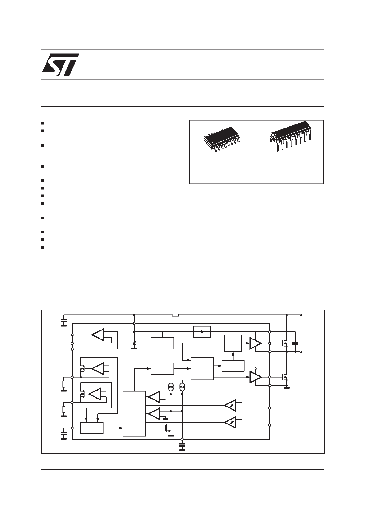
BLOCK DIAGRAM
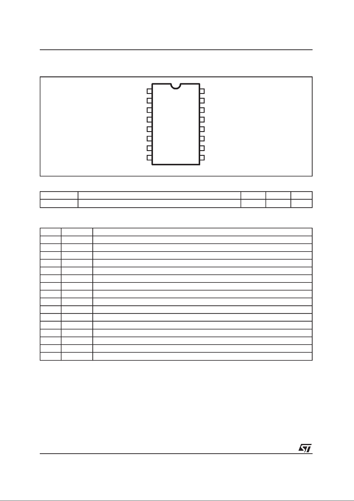
SO16N DIP16
ORDERING NUMBERS:
L6574D L6574
L6574
CFL/TL BALLAST DRIVER PREHEAT AND DIMMING
1/9
THERMAL DATA
Symbol Parameter DIP16 SO16N Unit
R
th j-amb
Thermal ResistanceJunction to ambient Max. 80 120 °C/W
PINS DESCRIPTION
N. Name Function
1 Cpre Preheat Timing Capacitor
2 Rpre Maximum Oscillation Frequency Setting. Low Impedence Voltage Source. See also Cf
3 Cf Oscillator Frequency Setting(see also Ring, Rpre)
4 Ring Minimum Oscillation FrequencySetting. Low Impedence Voltage Source. See also Cf
5 OPout Sense OP AMP Output. Low Impedence
6 OPin- Sense OP Amp Inverting Input. High Impedence
7 OPin+ Sense OP AMP Non Inverting InputHigh Impedence.
8 EN1 Half Bridge Enable
9 EN2 Half Bridge Enable
10 GND Ground
11 LVG Low Side Driver Output
12 Vs Supply Voltage with Internal Zener Clamp.
13 N.C. Non Connected
14 OUT High Side Driver Reference
15 HVG High Side Driver Output
16 Vboot Bootstrapped Supply Voltage
CPRE
RPRE
CF
RING
OPOUT
OPIN+
OPIN-
1
3
2
4
5
6
7 GND
V
S
LVG
N.C.
OUT
HVG
VBOOT16
15
14
13
12
10
11
D97IN492
EN1 8 EN29
PIN CONNECTION
L6574
2/9
ELECTRICALCHARACTERISTICS(VS= 12V; V
BOOT-VOUT
=12V; T
amb
=25°C)
Symbol Pin Parameter Test Condition Min. Typ. Max. Unit
Supply Voltage
V
suvp
12 VsTurn On Threshold 9.5 10.2 10.9 V
V
suvn
VsTurn Off Threshold 7.3 8 8.7 V
V
suvh
Supply Voltage Under Voltage
Hysteresys
2.2 V
V
cl
Supply Voltage Clamping 14.6 15.6 16.6 V
I
su
Start Up Current VS<V
suvn
250 µA
I
q
Quiescent Current,
fout = 60kHz, no load.
Vs > V
supv
2mA
High voltage Section
I
bootleak
16 BOOT pinleakage current V
BOOT
= 580V 5
µ
A
I
outleak
14 OUT pin Leakage Current V
OUT
= 562V 5
µ
A
High/Low Side Drivers
I
hvgso
15 High SideDriver Source Current V
HVG-VOUT
= 0 170 250 mA
I
hvgsi
15 High SideDriver Sink Current V
HVG-VBOOT
= 0 300 450 mA
I
hvgso
11 Low SideDrive Source Current VLVG-GND = 0 170 250 mA
I
lvgsi
11 Low SideDrive Source Current V
LVG-VS
= 0 300 450 mA
t
rise
15,11Low/High Side Output Rise Time C
load
= 1nF 80 120 ns
t
fall
Low/High Side Output Fall Time C
load
= 1nF 50 80 ns
ABSOLUTE MAXIMUM RATINGS
Symbol Parameter Value Unit
I
S
Supply Current(*) 25 mA
V
LVG
Low SideOutput -0.3 toVs +0.3 V
V
OUT
High SideReference -1 to VBOOT -18 V
V
HVG
High SideOutput -1 to VBOOT V
V
BOOT
Floating Supply Voltage -1 to 618 V
dV
BOOT
/dt V
BOOT
pin Slew rate (repetitive) ±50 V/ns
dV
OUT
/dt OUT pin Slew Rate (repetitive) ±50 V/ns
V
ir
Forced Input Voltage (pins Ring, Rpre) -0.3 to 5 V
V
ic
Forced Input Voltage (pins Cpre, Cf) -0.3 to 5 V
V
EN1,VEN2
Enable Input Voltage -0.3 to 5 V
I
EN1,IEN2
Enable Input Current ±3mA
V
opc
Sense Op Amp Common Mode Range -0.3 to 5 V
V
opd
Sense Op Amp DifferentialMode Range ±5V
V
opo Sense Op Amp Output Voltage (forced) 4.6 V
T
stg,Tj
Storage Temperature -40 to +150 °C
T
amb
Ambient Temperature -40 to +125 °C
(*) The device has an internal Clamping Zener between GND and the Vcc pin, it must not be suppliedby a Low Impedance VoltageSource.
Note: ESD immunity for pins14,15 and 16 is guaranteed up to 900V (Human Body Model)
RECOMMENDED OPERATING CONDITIONS
Symbol Parameter Value Unit
V
S
Supply Voltage 10 to VCL V
V
OUT
(*) High Side Reference -1 toVBOOT-VCL V
V
BOOT
(*) Floating Supply Voltage 500 V
(*) If the condition Vboot - Vout < 18 is guaranteed, Vout can range from -3 to 580V.
L6574
3/9

High/Low Side Driving Section:
High and low side driving sections provide the
proper drive to the external power MOSFET. A
high sink/sourcedrivingcurrent (450/250 mA typical) ensures fast switching times when a size 4
external power MOSFET needs to be driven.
BootstrapSection:
A patented integrated bootstrap section replaces
an external bootstrap diode. This section together with a bootstrap capacitor provides the
bootstrap voltage to drive the high side power
MOSFET. This function is achieved using a high
voltage DMOS driver which is driven synchronously with the low side externalpower MOSFET.
For a safe operation, current flow into the Vboot
pin is inhibited, even though ZVS operation may
not be ensured.
Timing Section:
To set the proper preheat time (tpre=kpre*Cpre)
for the bulb, a capacitor is connected to the Cpre
pin which is charged with a fixed current. During
tpre, the output is switching at fpre (see Oscillator
Section). When the tpre expires, the Cpre capacitor is discharged and then recharged with a
different current. This sets a second time interval
tsh (0.1 times the selected preheat time tpre) during which frequency shifting from fpre to fing is
performedto ensure lamp ignition.
OscillatorSection:
A voltage controlled oscillator, with the selected
frequencies fpre and fing, drives the output half
bridge. Independently selected, fpre is effective
during tpre and fing is effective during normal
lamp burning. When working open loop, fpre and
Symbol Pin Parameter Test Condition Min. Typ. Max. Unit
Oscillator
D
C
14 Output Duty Cycle 48 50 52 %
f
ing
Minimum OutputOscillation
Frequency
CF= 470pF;
R
ing
= 50kΩ
58.2 60 61.8 kHz
f
pre
Maximum Output Oscillation
Frequency
CF= 470pF;
R
ing
= 50kΩ;
R
pre
= 47kΩ
114 120 126 kHz
V
ref
2,4 Voltage to current converters
threshold
2V
t
d
14 Dead Time between Low and High
Side Conduction
0.8 1.25 1.7
µ
s
Timing Section
k
pre
1 Pre Heat Timing constant C
pre
= 330nF 1.15 1.5 1.85 s/µF
k
fs
Frequency Shift Timing Constant C
pre
= 330nF 0.115 0.15 0.185 s/µF
V
thpre
Pre HeatTiming Comparator
Threshold
3.3 3.5 3.7 V
Sense OP AMP
l
ib
6,7 Input Biascurrent 0.1
µ
A
V
io
Input OffsetVoltage -10 10 mV
R
out
5 Ouput Resistance 200 300 Ω
I
out +
Sink OutputCurrent V
out
= 0.2V 0.5 mA
I
out
- Source Output Current V
out
= 4.5V 0.5 mA
V
ic
6,7 Common Mode Input Range -0.2 3 V
GBW Sense Op Amp Gain Band Width
Product
1MHz
Gdc DC Open Loop Gain 80 dB
Comparators
V
the
8,9 Enabling Comparators Threshold 0.56 0.6 0.64 V
V
hye
Enabling Comparators Hysteresis 20 100 mV
t
pulse
Minimum Pulselenght 200 ns
ELECTRICALCHARACTERISTICS
(Continued)
L6574
4/9

fing are the highestand lowest allowed oscillation
frequencies.
Closed loop control of the lamp current under
normal operation can be achieved with the
L6574. This is accomplished by automatic adjustment of the oscillator frequency. The OP
AMP output is fed through a resistor diode network to the Ring pin. See AN993.
OP AMP Section:
The integrated OP AMP offers low output impedance, wide bandwidth, high input impedance and
wide common mode range. It can be readily
used to implementclosed loop control (see Oscillator Section) of the lamp current.
EN1, EN2 Comparators:
Two CMOS comparators, with thresholds set at
0.6 V (typical) are available to implement protection methods (such as overvoltage, lamp removal, etc.). Short pulses (>200nsec) at the
comparatorinputs are recognized.
The EN1 input (active high) forces the L6574 in
the shut down state (e.g. LVG low, HVG low, oscillator stopped) in the event of an undervoltage
condition. Normal operatingcondition is resumed
after a power-off power-on sequence or when
EN2 input is high.
The EN2 input (active high) also restarts a preheat sequence(see timingdiagrams).
V
CC
LVG
HVG
EN1
V
SUVP
D97IN490
TIMING DIAGRAMS
V
CC
t
PRE
t
PREtSH
t
SH
f
PRE
f
ING
EN2
f
OUT
V
SUVP
D97IN491B
TIMING DIAGRAMS
L6574
5/9

20 40 60 80 100 R
ING
(KΩ)
20
40
60
80
100
f
ING
(KHz)
D98IN867
Figure 1. f
ING
vs. R
ING
.
20 40 60 80 100 R
PRE
(KΩ)
20
40
60
80
100
∆
f
(KHz)
D98IN869
RING=50KΩ
Figure 3. ∆f vs. R
PRE
, withR
ING
= 50kΩ
-50 0 50 100
40
50
60
70
D98IN871
T(°C)
f
ING
(KHz)
Figure 5. f
ING
vs. temperature.
20 40 60 80 100 R
PRE
(KΩ)
20
40
60
80
∆
f
(KHz)
D98IN868
RING=33KΩ
Figure 2.∆f vs. R
PRE
, withR
ING
= 33k
Ω
20 40 60 80 100 R
PRE
(KHΩ)
20
40
60
80
100
∆
f
(KHz)
D98IN870
RING=100KΩ
Figure 4. ∆f vs. R
PRE
, withR
ING
= 100kΩ
-50 0 50 100
100
110
120
130
D98IN872
T(°C)
f
PRE
(KHz)
Figure 6. f
PRE
vs. temperature.
L6574
6/9

SO16 Narrow
DIM.
mm inch
MIN. TYP. MAX. MIN. TYP. MAX.
A 1.75 0.069
a1 0.1 0.25 0.004
0.009
a2 1.6 0.063
b 0.35 0.46 0.014 0.018
b1 0.19 0.25 0.007 0.010
C 0.5 0.020
c1 45°(typ.)
D (1) 9.8 10 0.386 0.394
E 5.8 6.2 0.228 0.244
e 1.27 0.050
e3 8.89 0.350
F (1) 3.8 4 0.150 0.157
G 4.6 5.3 0.181 0.209
L 0.4 1.27 0.016 0.050
M 0.62 0.024
S
(1) D and F do not include mold flash or protrusions. Mold flash or potrusions shall not exceed 0.15mm (.006inch).
OUTLINE AND
MECHANICAL DATA
8°(max.)
L6574
7/9

DIP16
DIM.
mm inch
MIN. TYP. MAX. MIN. TYP. MAX.
a1 0.51 0.020
B 0.77 1.65 0.030 0.065
b 0.5 0.020
b1 0.25 0.010
D 20 0.787
E 8.5 0.335
e 2.54 0.100
e3 17.78 0.700
F 7.1 0.280
I 5.1 0.201
L 3.3 0.130
Z 1.27 0.050
OUTLINE AND
MECHANICAL DATA
L6574
8/9

Information furnished is believed to be accurate and reliable. However, STMicroelectronics assumes no responsibility for the consequences
of use of such information nor for any infringement of patents or other rights of third parties which may result from its use. No license is
granted by implication or otherwise under any patent or patent rights of STMicroelectronics. Specification mentioned in this publication are
subject to change without notice. This publication supersedes and replaces all information previously supplied. STMicroelectronics products
are not authorized for use as critical components in life support devices or systems without express written approval of STMicroelectronics.
The ST logo is a registered trademark of STMicroelectronics
2000 STMicroelectronics – Printed in Italy – All Rights Reserved
STMicroelectronics GROUP OFCOMPANIES
Australia - Brazil - China - Finland - France - Germany - Hong Kong - India - Italy - Japan - Malaysia - Malta - Morocco -
Singapore - Spain - Sweden - Switzerland - UnitedKingdom - U.S.A.
http://www.st.com
L6574
9/9
 Loading...