

L6571A
TECHNOLOGY: BCD ”OFF-LINE”
FLOATINGSUPPLY VOLTAGEUPTO600V
GND REFERRED SUPPLY VOLTAGE UP TO
18V
DRIVER CURRENT CAPABILITY:
- SINK CURRENT = 270mA
- SOURCECURRENT=170mA
VERYLOW START UP CURRENT:150µA
VERYLOW OPERATINGCURRENT:<2mA
UNDERVOLTAGELOCKOUT
PROGRAMMABLEOSCILLATOR
FREQUENCY
dV/dtIMMUNITY UP TO ±50V/ns
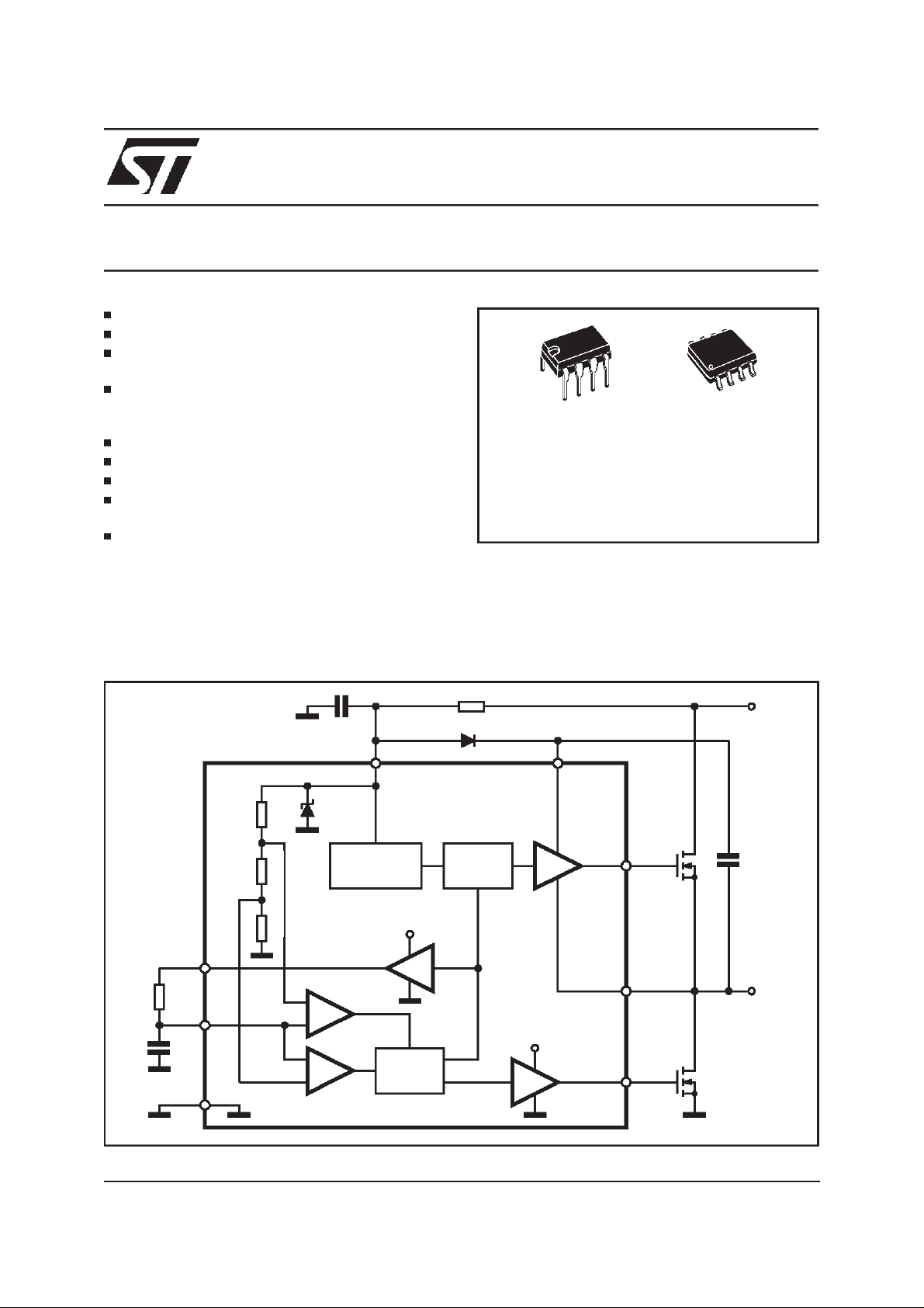
DESCRIPTION
The device is a high voltage half bridge driver
with built-in oscillator.The frequency of the oscillator can be programmed using external resistor
L6571B
HIGH VOLTAGE HALF BRIDGE
DRIVER WITH OSCILLATOR
Minidip SO8
ORDERING NUMBERS:
L6571A L6571AD
L6571B L6571BD
and capacitor.
The output drivers are designed to drive external
n-channel power MOSFET and IGBT. The internal logic assures a minimum dead time to avoid
cross-conductionof thepower devices.
BLOCK DIAGRAM
F
R
F
C
F
C
F
GND
C
VS
REGULATOR
BUFFERR
COMP
COMP
BIAS
S
V
S
LOGIC
R
HV
LEVEL
SHIFTER
H.V.
BOOTV
V
S
LOW
HIGH
SIDE
DRIVER
SIDE
DRIVER
HVG
OUT
LVG
C
BOOT
LOAD
June 2000
D96IN433
1/7
L6571A - L6571B
ABSOLUTE MAXIMUM RATINGS
Symbol Parameter Value Unit
(*)
I
S
V
CF
V
LVG
V
OUT
HVG High Side Switch Gate Output -1 to VBOOT V
V
BOOT Floating Supply Voltage 618 V
V
BOOT/OUT Floating Supply vs OUT Voltage 18 V
V
dV
BOOT
/dt V
dV
OUT
T
stg
T
j
T
amb
(*)
The device has an internal zener clamp between GND andVS(typical 15.6V).
Therefore the circuit should not be driven by a DC low impedance power source.
Note: ESD immunity for pins 6, 7 and 8is guaranteed up to900 V (Human Body Model)
Supply Current 25 mA
Oscillator Resistor Voltage 18 V
Low Side Switch Gate Output 14.6 V
High Side Switch Source Output -1 to V
/dt V
Slew Rate (Repetitive)
BOOT
Slew Rate (Repetitive)
OUT
BOOT
50 V/ns
±
50 V/ns
±
Storage Temperature -40 to 150
Junction Temperature -40 to 150
Ambient Temperature (Operative) -40 to 125 °C
-18 V
C
°
C
°
THERMAL DATA
Symbol Parameter Minidip SO8 Unit
R
th j-amb
Thermal ResistanceJunction-Ambient Max 100 150
RECOMMENDED OPERATINGCONDITIONS
Symbol Parameter Min. Max. Unit
Supply Voltage 10 V
CL
Floating Supply Voltage - 500 V
High Side Switch Source Output -1 V
BOOT-VCL
Oscillation Frequency 200 kHz
V
V
V
S
BOOT
OUT
f
out
PIN CONNECTION
V
RF
C
GND
S
F
1
2
3
4 LVG
7
6
5
BOOT8
HVG
OUT
C/W
°
V
V
2/7
D94IN059
L6571A - L6571B
ELECTRICALCHARACTERISTICS
(V
S
=12V;V
BOOT-VOUT
=12V;Tj =25°C;unlessotherwisespecified.)
Symbol Pin Parameter Test Condition Min. Typ. Max. Unit
V
SUVP
V
SUVN
V
SUVH
V
CL
I
SU
I
q
I
BOOTLK
1VSTurn On Threshold 8.3 9 9.7 V
VSTurn Off Threshold 7.3 8 8.7 V
VSHysteresis 0.7 1 1.3 V
VSClamping Voltage IS= 5mA 14.6 15.6 16.6 V
Start Up Current VS<V
Quiescent Current VS>V
8 LeakageCurrent BOOT pinvs
SUVN
SUVP
V
= 580V 5 µA
BOOT
150 250 µA
500 700 µA
GND
I
OUTLK
I
HVG SO
I
HVG SI
I
LVGSO
I
LVGSI
V
RFON
V
RF OFF
V
CFU
V
CFL
t
d
D
C
6 Leakage CurrentOUTpinvs GND V
7 High Side Driver Source Current V
High Side Driver Sink Current V
5 Low Side Driver Source Current V
Low Side Driver Sink Current V
= 562V 5
OUT
= 6V 110 175 mA
HVG
= 6V 190 275 mA
HVG
= 6V 110 175 mA
LVG
= 6V 190 275 mA
LVG
2 RF High LevelOutput Voltage IRF= 1mA VS-0.05 VS-0.2 V
RF Low Level Output Voltage IRF= -1mA 50 200 mV
3 CF Upper Threshold 7.7 7.95 8.2 V
CF Lower Threshold 3.80 4.05 4.3 V
Internal Dead Time L6571A
L6571B
Duty Cycle, Ratio Between
0.85
0.50
1.25
0.72
1.65
0.94
0.45 0.5 0.55
Dead Time + Conduction Time
of High Side and Low Side
Drivers
I
AVE
fout 6 Oscillation Frequency RT = 12k
1 Average Current from Vs No Load, fs = 60KHz 1.2 1.5 mA
57 60 63 kHz
CT = 1nF
µ
µ
µs
A
s
OSCILLATORFREQUENCY
The frequency of the internal oscillator can be
programmedusingexternalresistorand capacitor.
The nominal oscillator frequency can be calculated using the following equation:
Figure 2:
WAVEFORMS
V
S
V
CF
LVG
T1
T
f
OSC
=
2⋅R
1
⋅ C
F
F
⋅
In 2
=
1.3863⋅R
1
⋅
F
where RFand CFare the external resistor and capacitor
V
SUVP
C
D96IN434
C
F
3/7
 Loading...