

L6571A
TECHNOLOGY: BCD ”OFF-LINE”
FLOATINGSUPPLY VOLTAGEUPTO600V
GND REFERRED SUPPLY VOLTAGE UP TO
18V
DRIVER CURRENT CAPABILITY:
- SINK CURRENT = 270mA
- SOURCECURRENT=170mA
VERYLOW START UP CURRENT:150µA
VERYLOW OPERATINGCURRENT:<2mA
UNDERVOLTAGELOCKOUT
PROGRAMMABLEOSCILLATOR
FREQUENCY
dV/dtIMMUNITY UP TO ±50V/ns
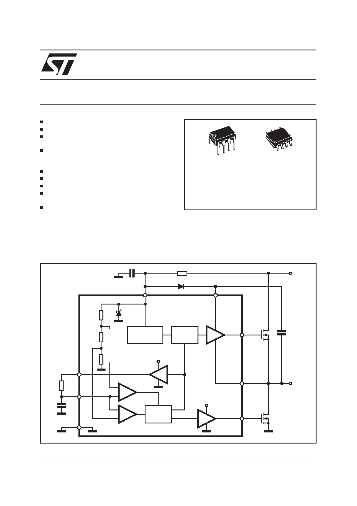
DESCRIPTION
The device is a high voltage half bridge driver
with built-in oscillator.The frequency of the oscillator can be programmed using external resistor
L6571B
HIGH VOLTAGE HALF BRIDGE
DRIVER WITH OSCILLATOR
Minidip SO8
ORDERING NUMBERS:
L6571A L6571AD
L6571B L6571BD
and capacitor.
The output drivers are designed to drive external
n-channel power MOSFET and IGBT. The internal logic assures a minimum dead time to avoid
cross-conductionof thepower devices.
BLOCK DIAGRAM
F
R
F
C
F
C
F
GND
C
VS
REGULATOR
BUFFERR
COMP
COMP
BIAS
S
V
S
LOGIC
R
HV
LEVEL
SHIFTER
H.V.
BOOTV
V
S
LOW
HIGH
SIDE
DRIVER
SIDE
DRIVER
HVG
OUT
LVG
C
BOOT
LOAD
June 2000
D96IN433
1/7
L6571A - L6571B
ABSOLUTE MAXIMUM RATINGS
Symbol Parameter Value Unit
(*)
I
S
V
CF
V
LVG
V
OUT
HVG High Side Switch Gate Output -1 to VBOOT V
V
BOOT Floating Supply Voltage 618 V
V
BOOT/OUT Floating Supply vs OUT Voltage 18 V
V
dV
BOOT
/dt V
dV
OUT
T
stg
T
j
T
amb
(*)
The device has an internal zener clamp between GND andVS(typical 15.6V).
Therefore the circuit should not be driven by a DC low impedance power source.
Note: ESD immunity for pins 6, 7 and 8is guaranteed up to900 V (Human Body Model)
Supply Current 25 mA
Oscillator Resistor Voltage 18 V
Low Side Switch Gate Output 14.6 V
High Side Switch Source Output -1 to V
/dt V
Slew Rate (Repetitive)
BOOT
Slew Rate (Repetitive)
OUT
BOOT
50 V/ns
±
50 V/ns
±
Storage Temperature -40 to 150
Junction Temperature -40 to 150
Ambient Temperature (Operative) -40 to 125 °C
-18 V
C
°
C
°
THERMAL DATA
Symbol Parameter Minidip SO8 Unit
R
th j-amb
Thermal ResistanceJunction-Ambient Max 100 150
RECOMMENDED OPERATINGCONDITIONS
Symbol Parameter Min. Max. Unit
Supply Voltage 10 V
CL
Floating Supply Voltage - 500 V
High Side Switch Source Output -1 V
BOOT-VCL
Oscillation Frequency 200 kHz
V
V
V
S
BOOT
OUT
f
out
PIN CONNECTION
V
RF
C
GND
S
F
1
2
3
4 LVG
7
6
5
BOOT8
HVG
OUT
C/W
°
V
V
2/7
D94IN059
L6571A - L6571B
ELECTRICALCHARACTERISTICS
(V
S
=12V;V
BOOT-VOUT
=12V;Tj =25°C;unlessotherwisespecified.)
Symbol Pin Parameter Test Condition Min. Typ. Max. Unit
V
SUVP
V
SUVN
V
SUVH
V
CL
I
SU
I
q
I
BOOTLK
1VSTurn On Threshold 8.3 9 9.7 V
VSTurn Off Threshold 7.3 8 8.7 V
VSHysteresis 0.7 1 1.3 V
VSClamping Voltage IS= 5mA 14.6 15.6 16.6 V
Start Up Current VS<V
Quiescent Current VS>V
8 LeakageCurrent BOOT pinvs
SUVN
SUVP
V
= 580V 5 µA
BOOT
150 250 µA
500 700 µA
GND
I
OUTLK
I
HVG SO
I
HVG SI
I
LVGSO
I
LVGSI
V
RFON
V
RF OFF
V
CFU
V
CFL
t
d
D
C
6 Leakage CurrentOUTpinvs GND V
7 High Side Driver Source Current V
High Side Driver Sink Current V
5 Low Side Driver Source Current V
Low Side Driver Sink Current V
= 562V 5
OUT
= 6V 110 175 mA
HVG
= 6V 190 275 mA
HVG
= 6V 110 175 mA
LVG
= 6V 190 275 mA
LVG
2 RF High LevelOutput Voltage IRF= 1mA VS-0.05 VS-0.2 V
RF Low Level Output Voltage IRF= -1mA 50 200 mV
3 CF Upper Threshold 7.7 7.95 8.2 V
CF Lower Threshold 3.80 4.05 4.3 V
Internal Dead Time L6571A
L6571B
Duty Cycle, Ratio Between
0.85
0.50
1.25
0.72
1.65
0.94
0.45 0.5 0.55
Dead Time + Conduction Time
of High Side and Low Side
Drivers
I
AVE
fout 6 Oscillation Frequency RT = 12k
1 Average Current from Vs No Load, fs = 60KHz 1.2 1.5 mA
57 60 63 kHz
CT = 1nF
µ
µ
µs
A
s
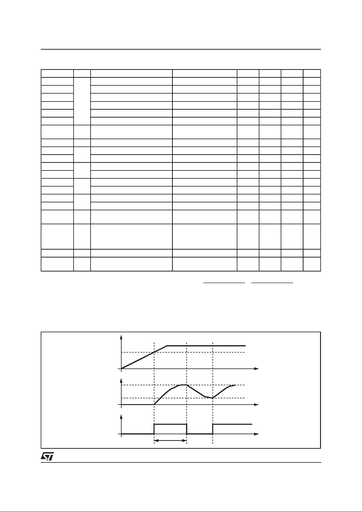
OSCILLATORFREQUENCY
The frequency of the internal oscillator can be
programmedusingexternalresistorand capacitor.
The nominal oscillator frequency can be calculated using the following equation:
Figure 2:
WAVEFORMS
V
S
V
CF
LVG
T1
T
f
OSC
=
2⋅R
1
⋅ C
F
F
⋅
In 2
=
1.3863⋅R
1
⋅
F
where RFand CFare the external resistor and capacitor
V
SUVP
C
D96IN434
C
F
3/7

L6571A - L6571B
Figure 3: TypicalDead Time vs.Temperature
Dependency(L6571A).
Dead time [µsec]
1.7
1.6
1.5
1.4
1.3
1.2
1.1
1
0.9
-50 0 50 100 150
Temperature [C]
Figure 5:
Typicaland Theoretical Oscillator
D96IN378A
Frequencyvs ResistorValue
f (KHz)
150
100
90
80
70
C=1nF
60
50
30
20
56789101520304050
C=330pF
C=560pF
Resistor Value (Kohm)
D96IN380
Theoretical
Figure4:
TypicalFrequency vs Temperature
Dependency
Frequency [KHz]
65
64
63
62
61
60
59
58
57
56
55
-50 -25 0 25 50 75 100 125
Temperature [C]
Figure8:
TypicalRise andFall Times vs. Load
Capacitance
time [nsec]
300
250
Tr
200
150
100
50
0
0123456
C [nF]
For both high andlow side buffers @25°C Tamb
Tf
D96IN379A
D96IN417
Figure 9: QuiescentCurrent vs. Supply Voltage.
D96IN418
4/7
Iq (µA)
4
10
3
10
2
10
10
02468101214VS(V)

L6571A - L6571B
DIM.
D (1) 4.8 5.0 0.189 0.197
F (1) 3.8 4.0 0.15 0.157
(1) D andF do not include moldflash or protrusions. Mold flash or
MIN. TYP. MAX. MIN. TYP. MAX.
A 1.75 0.069
a1 0.1 0.25 0.004 0.010
a2 1.65 0.065
a3 0.65 0.85 0.026 0.033
b 0.35 0.48 0.014 0.019
b1 0.19 0.25 0.007 0.010
C 0.25 0.5 0.010 0.020
c1 45° (typ.)
E 5.8 6.2 0.228 0.244
e 1.27 0.050
e3 3.81 0.150
L 0.4 1.27 0.016 0.050
M 0.6 0.024
S8°(max.)
potrusions shall not exceed0.15mm (.006inch).
mm inch
OUTLINE AND
MECHANICAL DATA
SO8
5/7
L6571A - L6571B
DIM.
MIN. TYP. MAX. MIN. TYP. MAX.
A 3.32 0.131
a1 0.51 0.020
B 1.15 1.65 0.045 0.065
b 0.356 0.55 0.014 0.022
b1 0.204 0.304 0.008 0.012
D 10.92 0.430
E 7.95 9.75 0.313 0.384
e 2.54 0.100
e3 7.62 0.300
e4 7.62 0.300
F 6.6 0.260
I 5.08 0.200
L 3.18 3.81 0.125 0.150
Z 1.52 0.060
mm inch
OUTLINE AND
MECHANICAL DATA
Minidip
6/7

L6571A - L6571B
Information furnished is believed to be accurate and reliable. However, STMicroelectronics assumesno responsibility for the consequences
of use of such information nor for any infringement of patents or other rights of third parties which may result from its use. No license is
granted by implication or otherwise under any patent or patent rights of STMicroelectronics. Specification mentioned in this publication are
subject to change withoutnotice. This publication supersedes and replaces all information previously supplied. STMicroelectronics products
are not authorized for use as critical components in life support devices or systems without express written approval of STMicroelectronics.
The ST logo is a registered trademark of STMicroelectronics
2000 STMicroelectronics – Printed in Italy – AllRights Reserved
STMicroelectronics GROUP OF COMPANIES
Australia - Brazil - China - Finland - France - Germany - HongKong - India - Italy - Japan - Malaysia - Malta - Morocco -
Singapore - Spain - Sweden - Switzerland - United Kingdom - U.S.A.
http://www.st.com
7/7
 Loading...