

SGS Thomson Microelectronics L6569D, L6569AD, L6569A, L6569 Datasheet
■
HIGH VOLTAGE RAIL UP TO 600V
■
BCD OFF LINE TECHNOLOGY
■
INTERNAL BOOTSTRAP DIODE
STRUCTURE
■ 15.6V ZENER CLAMP ON V
■
DRIVER CURRENT CAPABILITY:
S
- SINK CURRENT = 270mA
- SOURCE CURRENT = 170mA
■
VERY LOW START UP CURRENT: 150µA
■ UNDER VOLTAGE LOCKOUT WITH
HYSTERESIS
■
PROGRAMMABLE OSCILLATOR
FREQUENCY
■
DEAD TIME 1.25µs
■ dV/dt IMMUNITY UP TO ±50V/ns
■
ESD PROTECTION
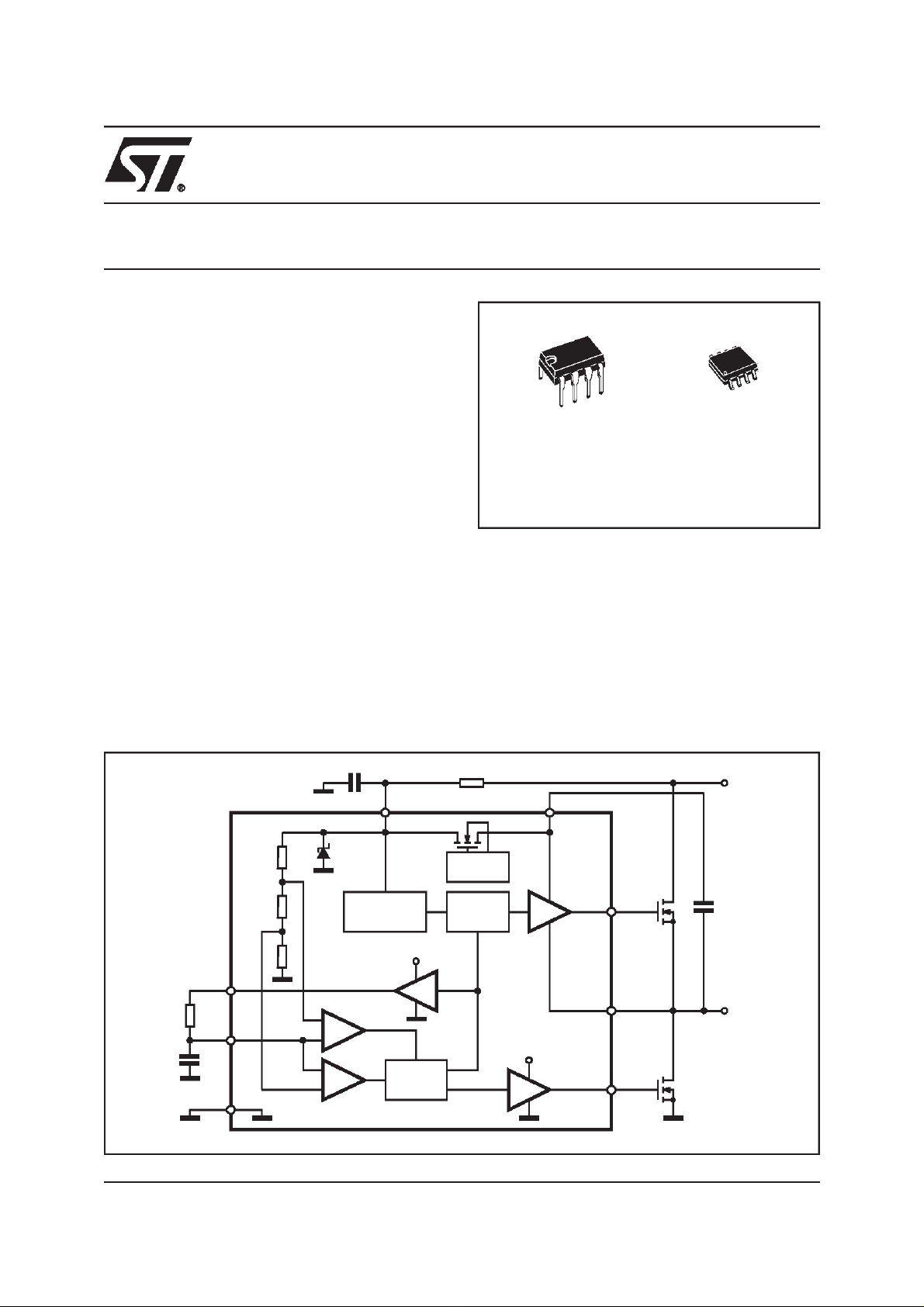
DESCRIPTION
The device is a high voltage half bridge driver with
built in oscillator. The frequency of the oscillator can
L6569
L6569A
HIGH VOLTAGE HALF BRIDGE
DRIVER WITH OSCILLATOR
Minidip SO8
ORDERING NUMBERS:
L6569 L6569D
L6569A L6569AD
be programmed using external resistor and capacitor. The internal circuitry of the device allows it to be
driven also by external logic signal.
The output drivers are designed to drive external nchannel power MOSFET and IGBT. Theinternal log-
µ
ic assures a dead time [typ. 1.25
conduction of the power devices.
Two version are available: L6569 and L6569A. They
differ in the low voltage gate driver start up sequence.
s] to avoid cross-
BLOCK DIAGRAM
R
C
VS
REGULATOR
2
F
R
F
C
3
F
C
F
GND
BUFFERR
COMP
COMP
S
18
Source
BIAS
V
S
LOGIC
June 2000
This ispreliminary information ona new product now in development. Details are subject to change without notice.
HV
CHARGE
PUMP
LEVEL
SHIFTER
BOOTV
HVG
7
HIGH
SIDE
DRIVER
OUT
6
V
S
LOW SIDE
DRIVER
LVG
54
D94IN058D
C
BOOT
H.V.
LOAD
1/13
L6569 L6569A
ABSOLUTEMAXIMUM RATINGS
Symbol Parameter Value Unit
(*) Supply Current 25 mA
I
S
V
CF
V
LVG
V
OUT
V
HVG
V
BOOT
V
BOOT/OUT
dV
BOOT
dV
OUT
T
stg
T
T
amb
(*)The device has an internal zener clamp between GND and VS (typical 15.6V).Therefore the circuit should not be driven by a DC low im-
pedance power source.
Note:
ESD immunity for pins 6, 7 and 8 is guaranteed up to 900 V (Human Body Model)
Oscillator Resistor Voltage 18 V
Low Side Switch Gate Output 14.6 V
High Side Switch Source Output -1 toV
High Side Switch Gate Output -1 to V
-18 V
BOOT
BOOT
Floating Supply Voltage 618 V
Floating Supply vs OUT Voltage 18 V
/dt VBOOT Slew Rate (Repetitive)
50 V/ns
±
/dt VOUT Slew Rate (Repetitive) ± 50 V/ns
Storage Temperature -40 to 150 °C
Junction Temperature -40 to 150 °C
j
Ambient Temperature (Operative) -40 to 125 °C
V
THERMAL DATA
Symbol Parameter Minidip SO8 Unit
R
th j-amb
Thermal Resistance Junction-Ambient Max 100 150 °C/W
RECOMMENDED OPERATINGCONDITIONS
Symbol Parameter Min. Max. Unit
Supply Voltage 10 V
CL
Floating Supply Voltage - 500 V
High Side Switch Source Output -1 V
BOOT-VCL
Oscillation Frequency 200 kHz
V
BOOT
V
V
S
OUT
f
out
PIN CONNECTION
V
RF
C
GND
S
F
1
2
3
4 LVG
7
6
5
BOOT8
HVG
OUT
V
V
2/13
D94IN059
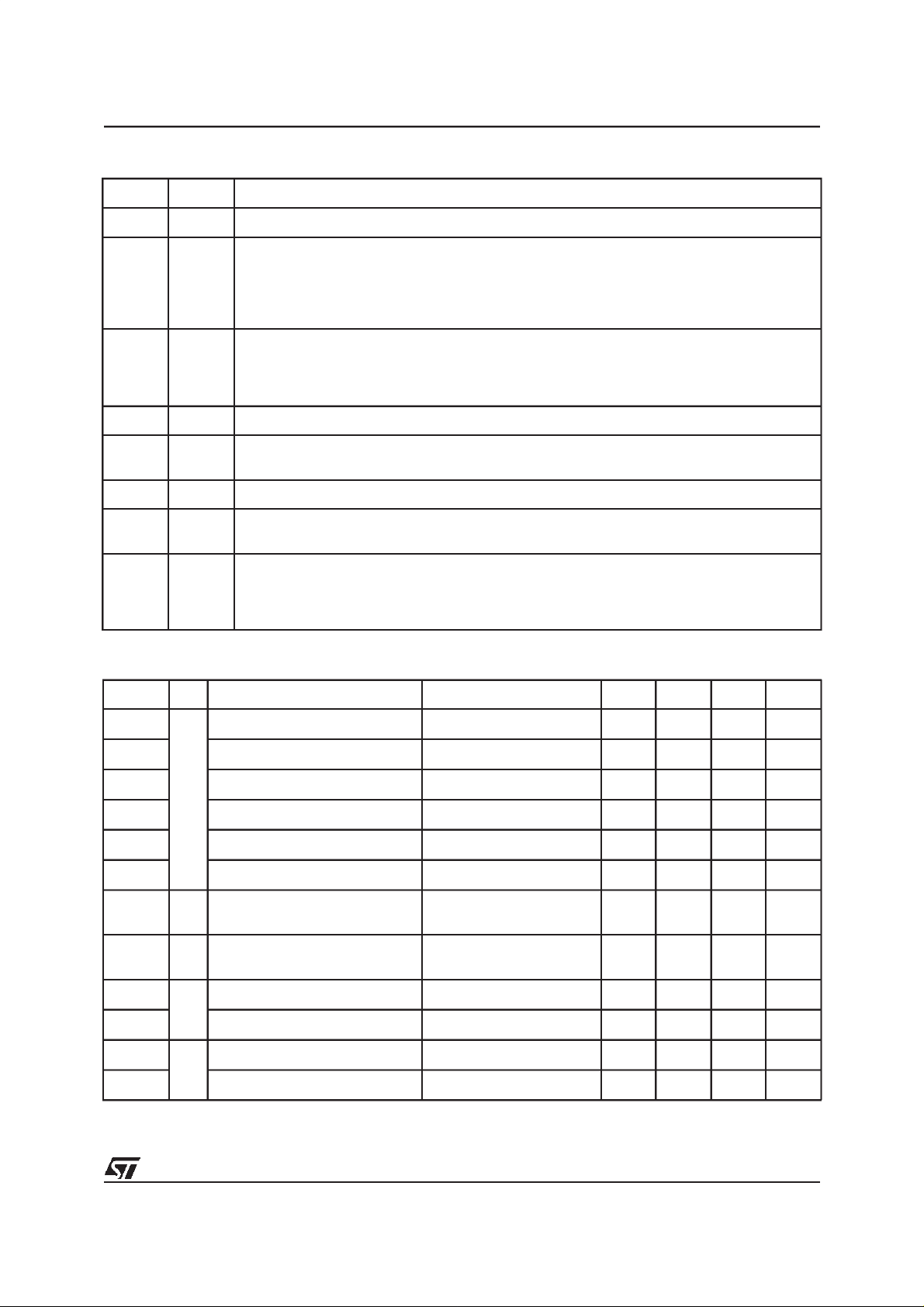
PIN FUNCTION
N° Pin Description
1 VS Supply input voltage with internal clamp [typ.15.6V]
L6569 L6569A
2 RF Oscillator timing resistor pin.
A buffer set alternatively to V
and GND can provide current to the external resistor RF
S
connected between pin 2 and 3.
Alternatively, the signal on pin 2 can be used also to driveanother IC (i.e. another L6569 to drive
a full H-bridge)
3 CF Oscillator timing capacitor pin.
A capacitor connected between this pin and GND fixes (together with R
) the oscillating
F
frequency
Alternatively an external logic signal can be applied to the pin to drive the IC.
4 GND Ground
5 LVG Low side driver output.
The output stage can deliver 170mA source and 270mA sink [typ.values].
6 OUT Upper driver floating reference
7 HVG High side driver output.
The output stage can deliver 170mA source and 270mA sink [typ.values].
8 BOOT Bootstrap voltage supply.
It is theupper driver floating supply. The bootstrap capacitor connected between this pin and pin
6 can be fed by an internal structure named “bootstrap driver” (a patented structure). This
structure can replace the external bootstrap diode.
ELECTRICAL CHARACTERISTCS
(VS=12V;V
BOOT-VOUT
=12V;Tj=25°C; unless otherwise specified.)
Symbol Pin Parameter Test Condition Min. Typ. Max. Unit
V
SUVP
V
SUVN
V
SUVH
V
CL
I
SU
I
q
I
BOOTLK
1 VS TurnOn Threshold 8.3 9 9.7 V
VS TurnOffThreshold 7.3 8 8.7 V
VS Hysteresis 0.7 1 1.3 V
VS Clamping Voltage IS= 5mA 14.6 15.6 16.6 V
Start Up Current VS<V
Quiescent Current VS>V
8 Leakage Current BOOT pin vs
GND
I
OUTLK
6 Leakage Current OUT pin vs
GND
I
HVGSO
I
HVG SI
I
LVG SO
I
LVG S
7 High Side Driver Source Current V
High Side Driver Sink Current V
5 Low Side Driver Source Current V
I Low Side Driver SinkCurrent V
SUVN
SUVP
V
= 580V 5
BOOT
V
= 562V 5
OUT
= 6V 110 175 mA
HVG
= 6V 190 275 mA
HVG
= 6V 110 175 mA
LVG
= 6V 190 275 mA
LVG
150 250
500 700
A
µ
A
µ
A
µ
A
µ
3/13
L6569 L6569A
ELECTRICAL CHARACTERISTCS (continued)
Symbol Pin Parameter Test Condition Min. Typ. Max. Unit
V
N 2 RF High Level Output Voltage IRF=1mA V
RFO
-0.05 V
S
-0.2 V
S
V
RF OFF
V
CFU
V
CFL
t
d
DC Duty Cycle, Ratio Between Dead
R
ON
V
BC
I
AVE
f
out
RF Low Level Output Voltage IRF= -1mA 50 200 mV
3 CF Upper Threshold 7.7 8 8.2 V
CF Lower Threshold 3.80 4 4.3 V
Internal Dead Time 0.85 1.25 1.65
0.45 0.5 0.55
Time + Conduction Time of High
Side and Low Side Drivers
On resistance of Boostrap
LDMOS
Boostrap Voltage before UVLO VS= 8.2 2.5 3.6 V
1 Average Current from Vs No Load, fs = 60KHz 1.2 1.5 mA
6 Oscillation Frequency RT= 12K; CT= 1nF 57 60 63 kHz
120
OSCILLATORFREQUENCY
The frequency of the internal oscillator can be programmed using external resistor and capacitor.
The nominal oscillator frequency can be calculated using the following equation:
f
OSC
------------- ------- ---------------------
2RFCFIn2
1
⋅⋅⋅
------------- --------- ------------------ --==
1.3863 RFC
1
⋅⋅
F
s
µ
Ω
Where R
and CFare the external resistor and capacitor.
F
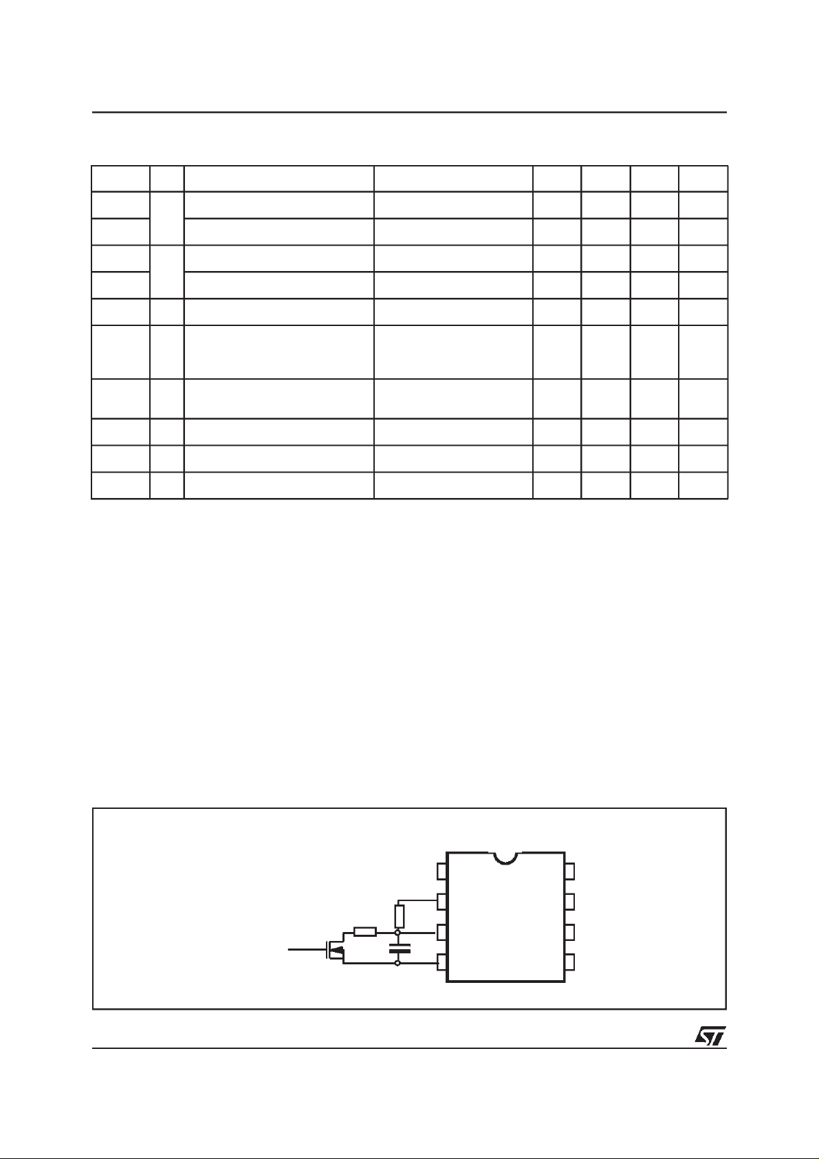
The device can be driven in ”shut down” condition keeping the C
taken:
1. When C
2. The forced discharge of the oscillator capacitor C
is to GND the high side driver is off and the low side is on
F
must not be shorter than 1us: a simple way to do this is to
F
limit the current discharge with a resistive path imposing R · C
Figure 1.
F
R
F
fault signal
R
C
GNDM
4/13
pin close to GND, but some cares have to be
F
>1µs (see fig.1)
F
1
2
3
4
8
7
6
5
 Loading...