

1/17
L6565
January 2003
■ QUASI-RESONANT (QR) ZERO-VOLTAGE-
SWITCHING (ZVS) TOPOLOGY
■ LINE FEED FORWARD TO DELIVER
CONSTANT POWER vs. MAINS CHANGE
■ FREQUENCY FOLDBACK FOR OP TI MU M
STANDBY EFFICI EN CY
■ PULSE-BY-PULSE & HICCUP-MODE OCP
■ ULTRA-LOW START-UP (< 70µA) AND
QUIESCENT CURRENT (< 3.5mA)
■ DISABLE FUNCTION (ON/OFF CONTROL)
■ 1% PRECISION (@ T
j
= 25°C) INTERNAL
REFERENCE VOLTAGE
■ ±400mA TO TE M POLE GATE DR IV E R WI TH
UVLO PULL-DOWN
■ BLUE ANGEL, ENERGY STAR, ENERGY
2000 COMPLIANT
APPLICATIONS
■ TV/MONITOR SMPS
■ AC-DC ADAPTERS/CHARGERS
■ DIGITAL CONSUMER
■ PRINTERS, FAX MACHINES,
PHOTOCOPIERS AND SCANNERS
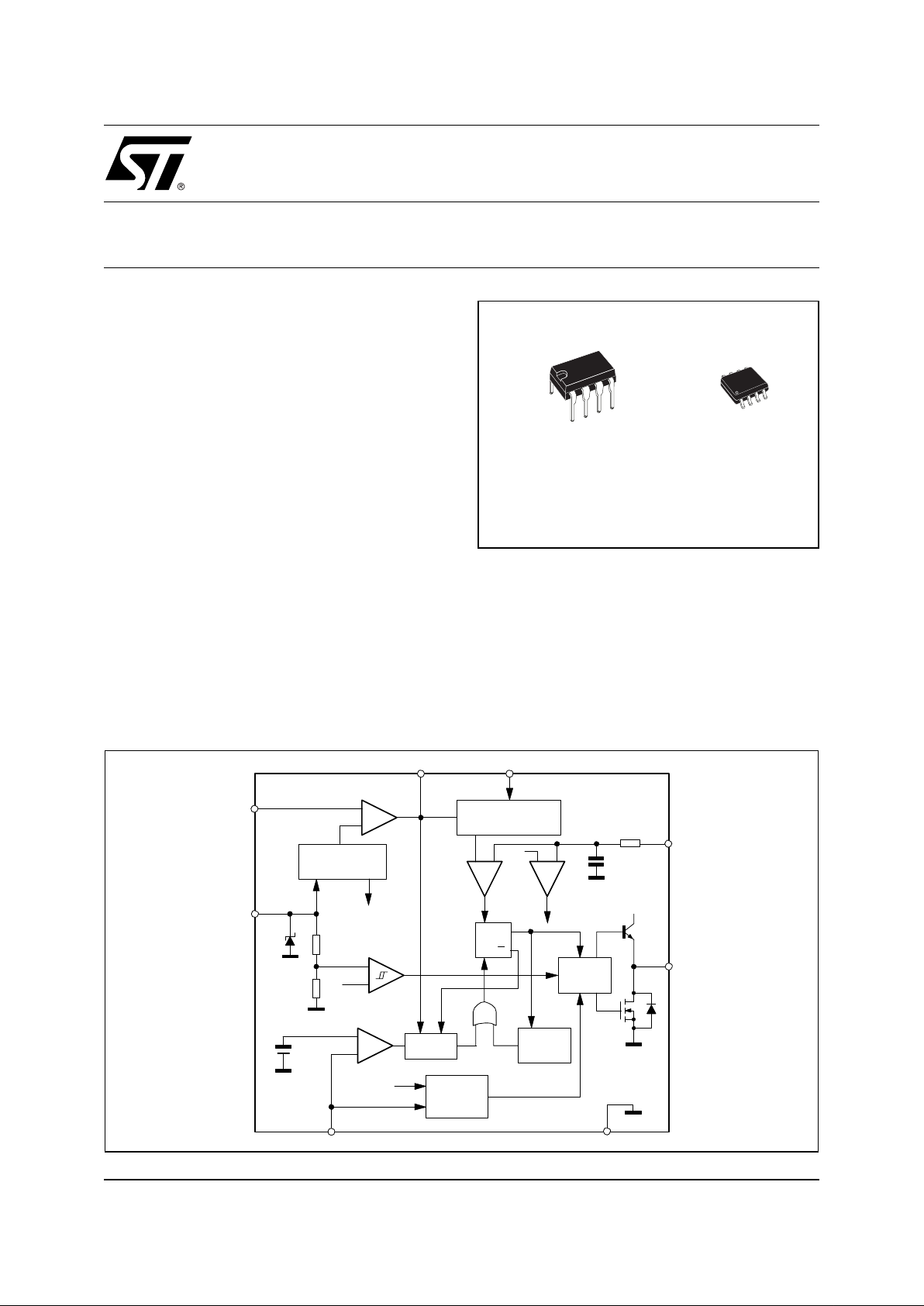
DESCRIPTION
The L6565 is a current-mode primary controller IC,
specifically designed to build offline Quasi-resonant
ZVS (Zero Voltage Switching at switch turn-on) flyback converters.
Quasi-resonant operation is achieved by means of a
transformer demagnetization sensing input that triggers MOSFET's turn-on.
DIP8(Minidip) SO-8
ORDERING NUMB ERS :
L6565N L6565D
QUASI-RESONANT SMPS CONTROLLER
BLOCK DIAGRAM
+
-
V
REF2
VOLTAGE
REGULATOR
INTERNAL
SUPPLY
+
-
2.5V
R1
R2
+-
DRIVER
+
-
ZERO CURRENT
DETECTOR
2.1V
1.6V
VCC8
1
23
4
ZCD
V
CC
INV
COMP
VFF
CS
GD
7
5
GND
6
20V
40K
5pF
BLANKING
LINE VOLTAGE
FEEDFORWARD
Hiccup-mode
OCP
DISABLE
RSQ
STARTER
2 V
+-
Hiccup-mode
OCP
Starter
STOP
Q
UVLO
Blanki ng
START
L6565
2/17
DESCRIPTION
(continued)
Converter's power capability variations with the mains voltage are compensated by line voltage feedforward.
At light load the device features a special function that automatically lowers the operating frequency still maintaining the operation as close to ZVS as possible. In addition to very low start-up and quiescent currents, this
feature helps keep low the consumption from the mains at light load and be Blue Angel and Energy Star compliant.
The IC includes also a disable function, an on-chip filter on current sense, an error amplifier with a precise reference voltage for primary regulation and an effective two-level overcurrent protection.
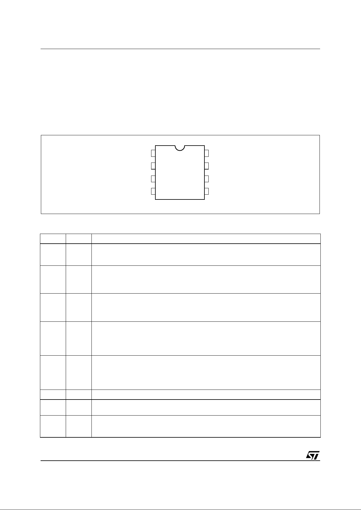
PIN CONNECTION
(Top view, Minidip and SO8)
PIN DESCRIPTION
N° Name Function
1 INV Inverting input of the error amplifier. The informatio n on the output voltage is fed into the pin
through either a res istor divider (primary reg ulation) or an optocoupler (second ary feedback).
This pin can be grounded in some secondary feedback schemes (see pin 2).
2 COMP Output of the error amplifie r. Typically, a compensat ion network is placed between this pin and
the INV pin to a chieve stability and good dy namic per forman ce o f the voltage con trol lo op. With
secondar y feedback, the pin can be also driven directly by an optocoupler to control PWM by
modulating the current sunk from the pin (with the INV pin grounded).
3 VFF Line voltage feedforward. The information on the converter’s input voltage is fed into the pin
through a resistor divider and is used to change the setpoint of the pulse-by-pulse current
limitation (the higher the voltage, the lower the setpoint). If this function is not desired the pin will
be grounded and the current limitation setpoint will be maximum.
4 CS Input to the P WM comparator. The primar y current is sense d through a resistor, the result ing
voltage is applied to this pin and co mpared with an inter nal reference to determ ine MOSFET’s
turn-off. The inter nal reference is clamped at a value, which defines the pulse-by-pulse current
limitation setpo int, d epen ding on th e voltage at p in VF F. If the sig nal a t the pin C S exceeds 2 V,
the gate driver will be disabled (Hiccup-mode OCP).
5 ZCD Transformer’s demagnetization sensing input for Quasi-Resonant operation. Alternately,
synchronizatio n input for an external signal. A nega tive-going edge triggers MO SFET’s turn- on.
The trigger cir cuit is blanked for a minimum of 3 .5 µs after MO SFET tur n-off, for safe operation
under short circuit conditions and frequency foldback. If the pin is grounded the IC will be
disabled.
6 GND Ground. Current return for both the signal part of the IC and the gate driver.
7 GD Gate d river output. Th e totem pole output stag e is able to d rive power MOSFET ’s and IGBT’s
with a peak current of 400 mA (source and sink).
8 Vcc Supply Voltage of both the signal part of the IC and the gate driver. An electrolytic capacitor is
connected b etween this pin an d ground. A resist or connected from this pin to the converter’s
input bulk capacitor will be typically used to start up the device.
ZCD
INV
COMP
VFF
CS
Vcc
GD
GND
1
2
3
4
8
7
6
5
3/17
L6565
THERMAL DATA
ABSOLUTE MAXIMUM RATINGS
Symbol Parameter SO8 Minidip Unit
R
th j-amb
Max. Thermal Resistance, Junction-to-ambient 150 100 °C/W
Symbol Pin Parameter Value Unit
I
Vcc
8ICC + I
Z
30 mA
I
GD
7 Output Totem Pole Peak Current (2 µs) ±700 mA
INV, COMP,
VFF, CS
1, 2, 3 4 Analog Inputs & Outputs -0.3 to 7 V
I
ZCD
5 Zero Current Detector 50 (source)
-10 (sink)
mA
P
tot
Power Dissipation @T
amb
= 50°C (Minidip)
(SO8)
1
0.65
W
T
j
Junction Temperature Operating range -40 to 150 °C
T
stg
Storage Temperature -55 to 150 °C
ELECTRICAL CHARACTERISTCS
(Tj = -25 to 125°C, VCC = 12V, Co = 1nF; unless otherwise specified)
Symbol Parameter Test Condition Min. Typ. Max. Unit
SUPPLY VOLTAGE
V
cc
Operating range After turn-on 10.3 18
V
CCOn
Turn-on threshold 12.5 13.5 14 .5 V
V
CCOff
Turn-off threshold 8.7 9.5 10.3 V
Hys Hysteresis 3.65 4 4.3 V
V
Z
Zener Voltage Icc = 25 mA 18 20 22 V
SUPPLY CURRENT
I
start-up
Start-up Current
Before turn-on, V
CC
= 12V
45 70 µA
I
q
Quiescent Current After turn-on 2.3 3.5 mA
I
CC
Operating Supply Current @ 70 kHz 3.5 5 mA
I
q
Quiescent Current During Hiccup-mode OCP 1.6 3.5 mA
I
q
Quiescent Current V
ZCD
< V
DIS
, VCC>V
CCOff
1.4 2.1 mA
LINE FEEDFORWARD
I
VFF
Input Bias Current V
VFF
= 0 to 3 V -1 µA
V
VFF
Operating Range 0 to 3 V
K Gain
V
VFF
= 1.5V, V
COMP
= 4V
0.16
ERROR AMPLIFIER
V
INV
Voltage Feedback Input
Threshold
T
amb
= 25°C 2.465 2.5 2.535 V
12V < VCC < 18V 2.44 2.56
Line Regulation Vcc = 12 to 18V 2 5 mV
I
INV
Input Bias Current -0.1 - 1 µA
L6565
4/17
G
V
Voltage Gain Open loop 60 80 dB
GB Gain-Bandw idth Produ ct 1 MHz
I
COMP
Source Current V
COMP
= 4V, V
INV
= 2.4 V -2 -3.5 -5 mA
Sink Current V
COMP
= 4V, V
INV
= 2.6 V 2.5 4.5 mA
V
COMP
Upper Clamp Voltage I
SOURCE
= 0.5 mA 5 5.5 V
Lower Clamp Voltage I
SINK
= 0.5 mA 2.25 2.55 V
CURRENT SENSE COMPARATOR
I
CS
Input Bias Current VCS = 0 -0.05 -1 µA
t
d(H-L)
Delay to Output 200 450 ns
V
CSx
Current Sense Reference Clamp
V
COMP
= Upper clamp, V
VFF
= 0V
1.28 1.4 1.5 V
V
COMP
= Upper clamp, V
VFF
= 1.5V
0.62 0.7 0.78
V
COMP
= Upper clamp, V
VFF
= 3V
00.2
V
CSdis
Hiccup-mode OCP level 1.85 2.0 2.2 V
ZERO CURRENT DETECTOR/ SYNCHRONIZATION
V
ZCDH
Upper Clamp Voltage I
ZCD
= 3mA 4.7 5.2 6.1 V
V
ZCDL
Lower Clamp Voltage I
ZCD
= - 3mA 0.3 0.65 1 V
V
ZCDA
Arming Voltage
(positive-going edge)
(1)
2.1 V
V
ZCDT
Triggering Voltage
(negative-going edge)
1.6 V
I
ZCDb
Input Bias Current V
ZCD
= 1 to 4.5 V 2 µA
I
ZCDsrc
Source Current Capability -3 -10 mA
I
ZCDsnk
Sink Current Capability 3 10 mA
V
DIS
Disable Threshold 150 200 250 mV
I
ZCDr
Restart Current After Disable V
ZCD
< V
DIS
, Vcc > Vcc
off
-70 -150 -230 µA
T
BLANK
Blanking time after pin 7 high-tolow transition
V
COMP
≥ 3.2 V 3.5 µs
V
COMP
= 2.5 V 18
START TIMER
t
START
Start Timer period 250 400 550 µs
GATE DRIVER
V
OL
Dropout Voltage I
GDsource
= 200mA 1.2 2 V
I
GDsource
= 20mA 0.7 1
V
OH
I
GDsink
= 200mA 2 V
I
GDsink
= 20mA 0.3
t
f
Current Fall Time 40 100 ns
t
r
Current Rise Time 40 100 ns
I
GDoffIGD
sink current Vcc = 4 V, VGD = 1 V 5 10 mA
(1) Parame ters guaran teed by design, not tested i n production.
ELECTRICAL CHARACTERISTCS
(continued)
(T
j
= -25 to 125°C, VCC = 12V, Co = 1nF; unless otherwise specified)
Symbol Parameter Test Condition Min. Typ. Max. Unit
5/17
L6565
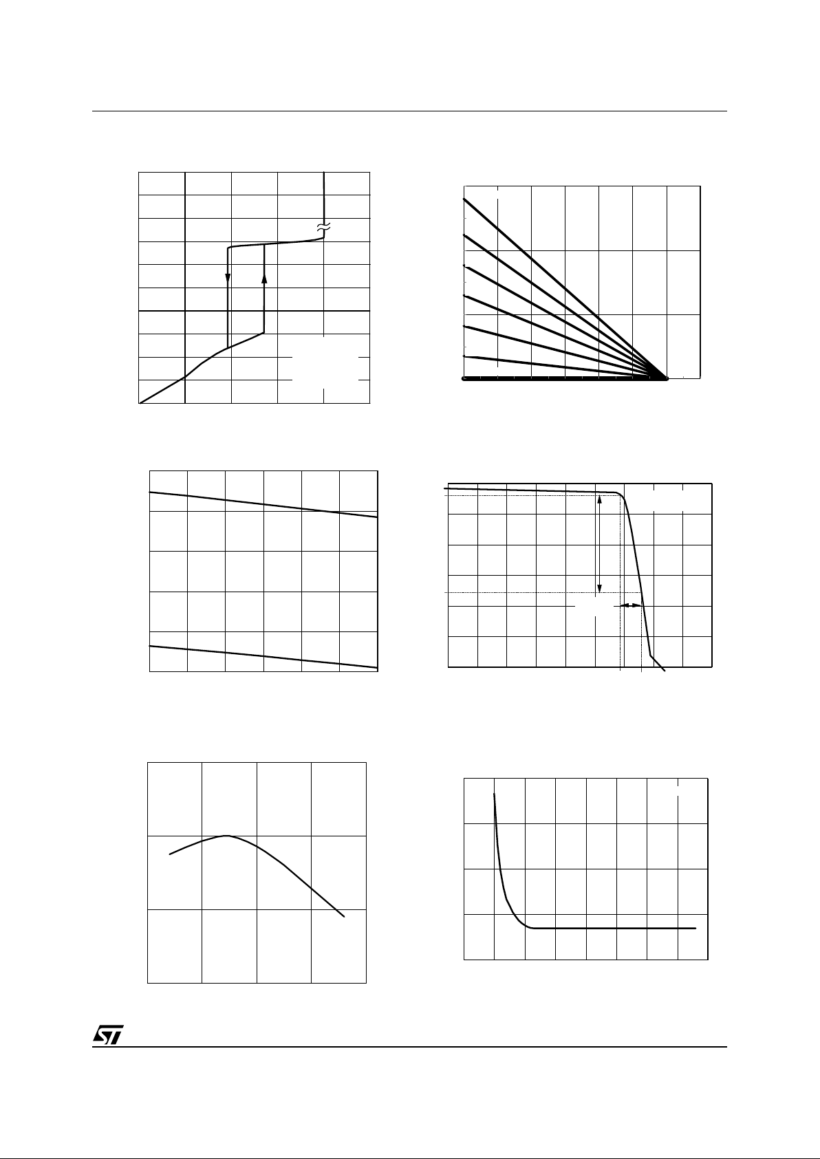
Figure 1. Supply current vs. Supply voltage
Figure 2. Start - up & U VL O vs . Tem perature
Figure 3. Fee dback referen ce v s. Te m pe rature
Figure 4. Line feedforward characteristics
Figure 5. Pin 2 (COMP) V-I characteristics
Figure 6. ZCD blanking time vs. COMP voltage
0 5 10 15 20 V
CC
(V)
0
0.005
0.01
0.05
0.1
0.5
1
5
10
I
CC
(mA)
CL = 1nF
f = 70KHz
TA = 25°C
T (°C)
V
CC-ON
(V)
V
CC-OFF
(V)
-25 0 25 50 75 100 125
9
10
11
12
13
14
-50 0 50 100
2.46
2.48
2.50
T (°C)
V
REF
(V)
D94IN048A
V
csx
[V]
0 0.5 1 1.5 2 2.5 3 3.5
0
0.5
1
1.5
V
VFF
[V]
VCOMP = 2.5V
3.0 V
3.5 V
4.0 V
4.5 V
5.0 V
Upper clamp
01234
0
1
2
3
4
5
6
Regulation
range
V
COMP
[V]
I
COMP
[mA]
Tj = 25 °C
Vpin1 = 0
T
BLANK
[µs]
23456
0
5
10
15
20
V
COMP
[V]
Tj = 25 °C
L6565
6/17
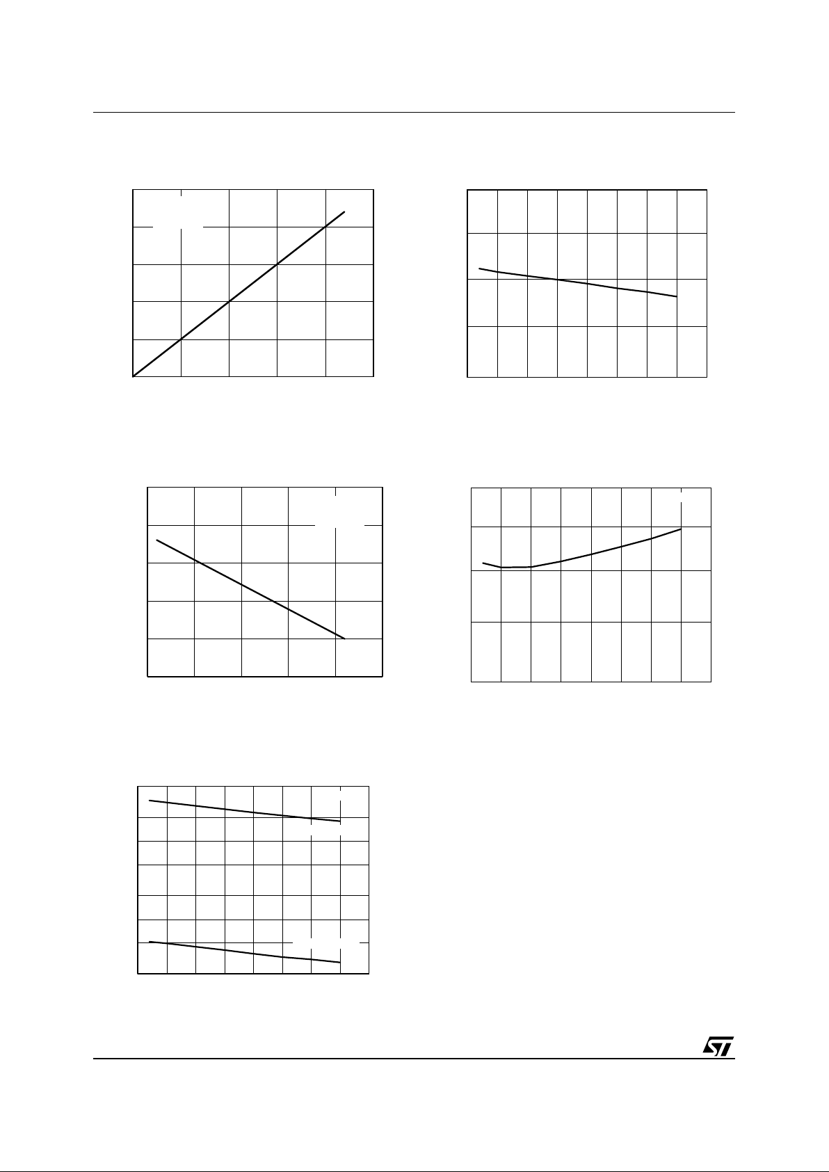
Figure 7. Gate-drive output saturation
Figure 8. Gate-drive output saturation
Figure 9. IC co nsumption vs . te m perature
Figure 10. Zener voltage at Vcc pin vs. Tj
Figure 11. Start-up timer period vs. Tj
V
pin7
[V]
0 100 200 300 400 500
0
0.5
1
1.5
2
2.5
IGD[mA]
Tj = 25 °C
Vcc = 14.5 V
SINK
V
pin7
[V]
0 100 200 300 400 500
-2.5
-2
-1.5
-1
-0.5
0
IGD[mA]
Tj = 25 °C
Vcc = 14.5 V
SOURCE
Vcc - 0.5
Vcc - 1.0
Vcc - 1.5
Vcc - 2.0
Vcc - 0.5
Vcc - 0.5
Icc [mA]
-50 0 50 100 150
0.02
0.05
0.1
0.2
0.5
1
2
5
Tj [°C]
Quiescent
Before Start-up
Vcc=12V
Vz [V]
-50 0 50 100 150
18
19
20
21
22
Tj [°C]
TSTART [µs]
-50 0 50 100 150
250
300
350
400
450
Tj [°C]
Vcc=12V
 Loading...