L6515
DUAL DC-MOTOR POSITIONING SYSTEM
ADVANCE DATA
PRECISE OPERATION ALSO WITH LOW
COST OPTICALENCODER
PWM - OUTPUT FOR DIGITAL SWITCHED
POWERBRIDGES
DIRECTION INDICATOR FOR EASY POSITIONCOUNTING WITH µP
EXTERNAL LOOP GAIN AND TRANSFER
FUNCTIONALADJUSTMENT
PARALLEL ADDRESSED INPUTS WITH
LATCH
44 LEAD PLCC PACKAGE
DESCRIPTION
The L6515 is a monolithic integrated circuit in
BCD-Technologyassembledina PLCC-44plastic
chipcarrier.
The device contains all functions for a complete
dual DC-Motor positioning system. For the motor
driver stage only digital switched bridges are
needed.
Useful are L293E, L298, L6203 and L6202. The
device is intended to drive DC-Motors in typewriters, printers, plotters and general purpose industrialapplications.
This isadvanced information on anew product now in development or undergoing evaluation. Details are subject tochange without notice.
May 1994
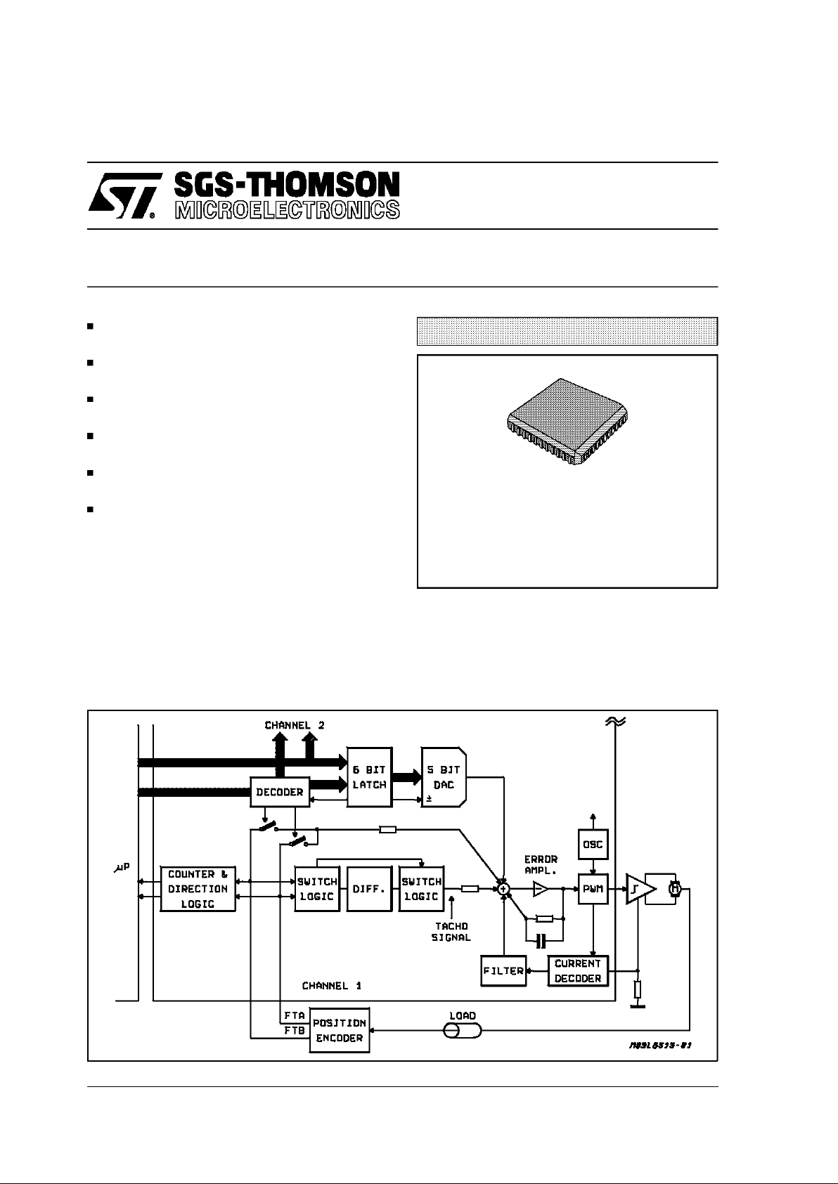
SYSTEM BLOCK DIAGRAM (ONECHANNEL)
PLCC44
ORDERING NUMBER: L6515
MULTIPOWERBCD TECHNOLOGY
1/13

SYSTEM DESCRIPTION
The L6515 is intended to be used as a microprocessorcontrolledpositioningsystem.
For the motor driver stage only digital operating
bridgesareneededl ikeL293E,L298,L6203,L6202.
The system operates in two modes to achieve
high-speed,high-accurancy positioning.
Speed commands for the system originate in the
microprocessor. It is continuouslyupdated on the
motor position by means of pulses from the controller chip, which in turn gets its information from
the encoder. From this basic input, the microprocessor computes a 6-bit control word that sets the
systemspeed anddirectiondependenton the distance to travel.
When the motor is stopped and the microprocessor orders it to a new position, the system oper-
ates initially in an open-loop configuration as
there is no feedback from the tachometer generator.Therefore maximumcurrentis fed to themotor. As maximum speed is reached, the tachometer chip output backs off the processors signal
thus reducing acceleratingtorque.Themotor continues to run at top speed but under closed-loop
control.
As a target position is approached,the microprocessor lowers the value of the speed-demand
word; this reduces the voltage at the main summing point, in effect braking the motor. The braking is appliedprogressively until the motor is running at minimum speed.
At that time, the microprocessor orders a switch
to the position mode, and within 3 to 4ms the
power stage drives the motor to a null position,
whereit is held by electronic ”detening”.
Symbol Parameter Value Unit
V
S
Supply Voltage 12 V
V
IA
Analog Inputs Voltage -0.3 to 7 V
V
IL
Logic Inputs Voltage -0.3 to 7 V
V
O
Open Collector Output Current 12 V
I
O
Open Collector Current 10 mA
I
Z
Zener Current 20 mA
T
stg
, Tj Storage Temperature -40to 150 °C
T
amb
Operative Ambient Temperature 0 to 70 °C
ABSOLUTE MAXIMUMRATINGS
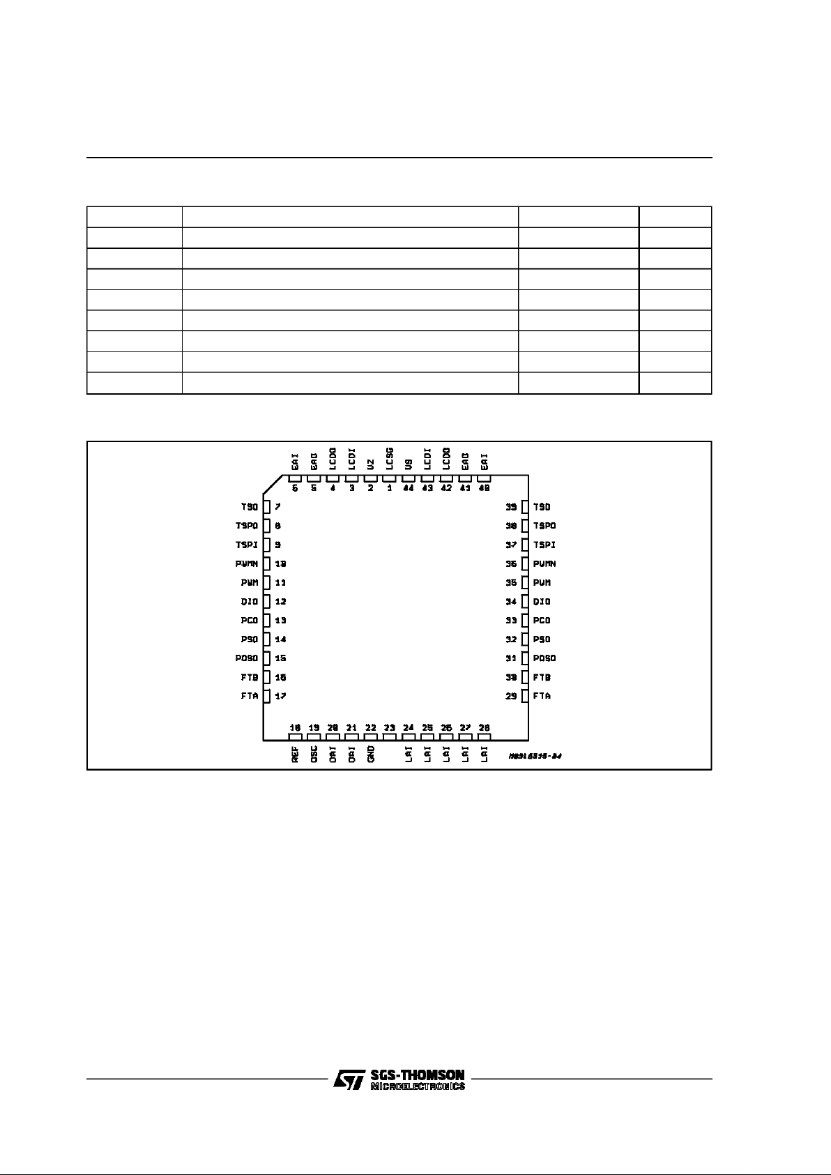
PIN CONNECTION (top view)
LAI
L6515
2/13

Pin Name Description
1 LCSG Load Current Decoder Sens Reference Ground
2V
Z
Zener Clamp
3,43 LCDI Load Current Decoder Input
4,42 LCDO Load Current Decoder Output
5,41 EAO Error AmplifierOutput for Current Mode PWM Modulator
6,40 EAI Error Amplifier Input for Current Mode PWM Modulator
7,39 TSO Tacho Signal Output
8,38 TSPO Tacho SignalProcessor Output
9,37 TSPI Tacho Signal Processor Input
10,36 PWMN Current Mode PWM Output Inverted
11,35 PWM Current Mode PWM Output non Inverted
12,34 DIO Direction Indicator Digital Open Collector Output. A Low Level is cw,
A High Level is ccw Operation ofthe Motor
13,33 PCO Position Counter Digital Open Collector Output
14,32 PSO Phase Selector Output for Signal Differentation
15,31 POSO Positioning Output. The Output Becomes Activated via Position
Adress Decoder.
16,30 FTB Analog Input from PositionEncoder Phase B. Proposed Operation
Range is 2.8V + 1V.
17,29 FTA Analog Input from PositionEncoder Phase A. Proposed Operation
Range is 2.8V + 1V
18 REF Master Current Reference
19 OSC Oscillator
20,21 DAI Decoder Logic Input for Latch Select + Reset
22 GND Major and Logic Ground
23 to 28 LAI Latch Adress Input
44 V
S
Supply Voltage
PIN FUNCTIONS
L6515
3/13

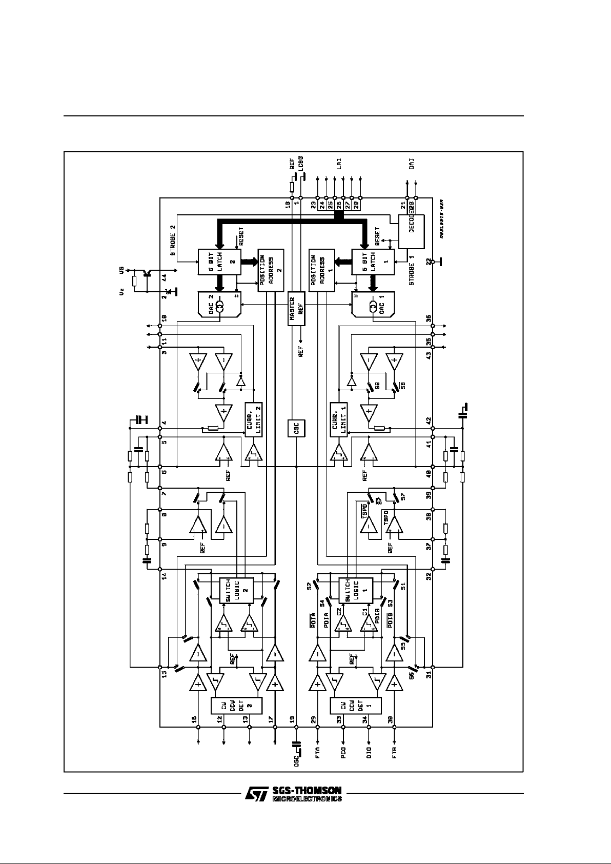
SCHEMATICDIAGRAM
L6515
4/13
 Loading...