

SGS Thomson Microelectronics L6506D, L6506 Datasheet
CURRENTCONTROLLERFOR STEPPING MOTORS
DESCRI P TI ON
The L6506/Dis a linearintegratedcircuit designed
to senseand controlthecurrentinsteppingmotors
and similardevices.Whenusedin conjunctionwith
the L293, L298, L7150,L6114/L6115,the chip set
formsa constantcurrentdrive foran inductiveload
andperformsalltheinterfacefunctionfromthe control logic thruthe powerstage.
Two or more devices may be synchronized using
thesyncpin.In thismodeof operationtheoscillator
in themasterchipsetstheoperatingfrequencyinall
chips.
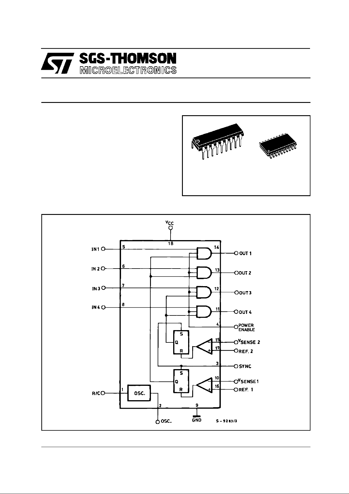
BLOCK DIAGRAM (pin’s number referred to DIP-18)
L6506
L6506D
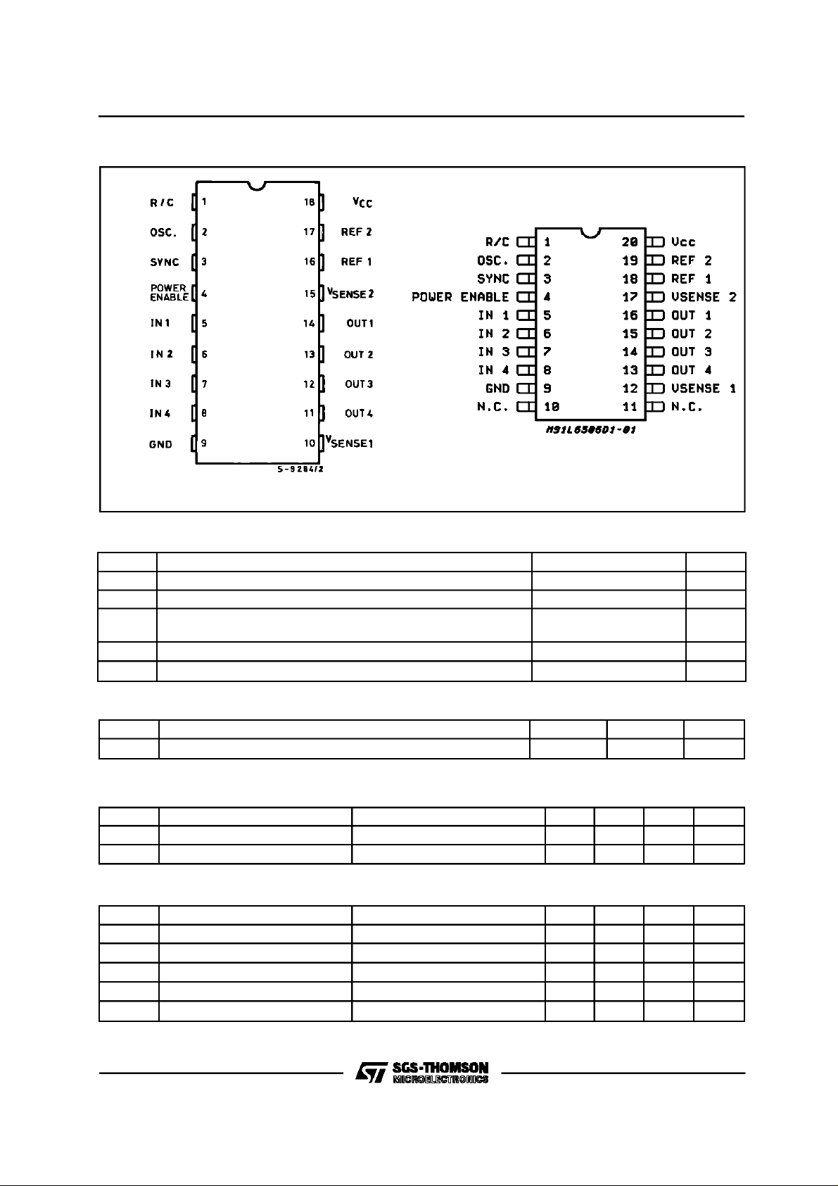
DIP18 SO20
ORDERING NUMBERS:
L6506 L6506D
June 1997
1/8
L6506 -L6506D
PI N CONNE CTI ONS (top view)
DIP18 SO20
ABSOLUTEMAXIMUM RATINGS
Symbol Parameter Val u e Uni t
V
V
P
T
T
Supply Voltage 10 V
CC
Input Signals 7 V
i
Total Power Dissipation(T
tot
=70°C) for DIP18
amb
Total Power Dissipation(Tamb =70ÉC) for SO20
JunctionTemperature 150
j
Storage Temperature -40 to 150
stg
1
0.8
THERMAL DATA
Symb o l Parameter DIP 18 SO 20 Uni t
R
thj-amb
ELECTRICAL CHARACTERESTICS (VCC= 5.0V,T
Thermal ResistanceJunction-ambient Max. 80 100
=25°C; unlessotherwisenoted)
amb
C/W
°
Symb o l Parameter Test Cond itions Mi n . Typ . Max. Unit
V
I
SupplyVoltage 4.5 7 V
CC
QuiescentSupplyCurrent VCC=7V 25 mA
CC
COMPARATOR SECTION
Symb o l Parameter Test Cond itions Mi n . Typ . Max. Unit
V
V
I
I
Input Voltage Range V
IN
Input Offset Voltage VIN= 1.4V
IO
Input Offset Current
IO
Input Bias Current 1 µ
IB
Response time V
Inputs –0.3 3 V
sense
±5.0
±200
REF
= 1.4V V
= 0 to 5V 0.8 1.5
SENS
W
W
C
°
°C
mV
nA
µ
A
s
2/8
L65 06 - L6506D
ELECTRICAL CHARACTERISTICS(continued)
COMPARATOR SECTIONPERFORMANCE(OverOperatingTemperatureRange)
Symbol Parameter Test Condtions Min. Typ. Max. Unit
V
Input Offset Voltage VIN= 1.4V
IO
Input Offset Curent
I
IO
±
±
500
20
mV
nA
LOGICSECTION
Symbol Parameter Test Condtions Min. Typ. Max. Unit
V
V
V
Input High Voltage 2 V
IH
Input Low Voltage 0.8 V
V
IL
Output High Voltage VCC= 4.75V
OH
Ouptut Low Voltage VCC= 4.75V
OL
Ouput Source Current - Outputs
I
OH
1-4
(OverOperatingTemperatureRange -TTL compatibleinputs& outputs)
2 3.5 V
= 400µA
I
OH
0.25 0.4 V
= 4mA
I
OH
VCC= 4.75V 2.75 mA
s
OSCILLATOR
Symbol Parameter Test Condtions Min. Typ. Max. Unit
f
V
V
Frequency Range 5 70 KHz
osc
Lower Threshold Voltage 0.33 V
thL
Higher Threshold Voltage 0.66 V
thH
Internal Discharge Resistor 0.7 1 1.3
R
i
CC
CC
CIRCUIT OP ERATION
TheL6506isintendedfor use withdual bridgedrivers,suchasthe L298,quaddarlingtonarrays,such
as the L7150, quad DMOS array such as L6114L6115,ordiscretepowertransistorstodrivestepper
motorsandothersimilarloads.Themainfunctionof
thedeviceistosenseandcontrolthecurrentineach
of theload windings.
Acommonon-chiposcillatordrivesthedualchopper
andsetsthe operatingfrequencyforthepulsewidth
modulateddrive.The RCnetworkon pin1 setsthe
operatingfrequencywhichis givenby the equation
:
f = forR > 10 K
1
0.69 RC
The oscillator provides pulses to set the two flipflopswhichin turncausethe outputsto activatethe
drive.Whenthecurrentintheloadwindingreaches
theprogrammedpeakvalue,thevoltageacrossthe
senseresistor (R
) is equal to V
sense
and the cor-
ref
respondingcomparatorresetsits flip-flopinterruptingthedrivecurrentuntilthenextoscillatorpulseoccurs. The peak current in each winding is programmedby selectingthe valueofthe senseresis-
tor and V
. Sinceseparateinputsare providedfor
ref
each chopper, each of the loads may be programmed independentlyallowing the device to be
used to implement microstepping of the motor.
LowerthresholdofL6506’soscillatoris 1/3V
per thresholdis 2/3 V
sistoris 1 KΩ ±
30%.
and internal dischargere-
CC
CC
Ground noise problems in multiple configurations
can be avoided by synchronizing the oscillators.
This may be done by connecting the sync pins of
eachof the deviceswith the oscillatoroutput of the
masterdeviceandconnectingtheR/Cpinoftheunusedoscillatorsto ground.
Theequationsfor the activetime of thesync pulse
(T2),the inactivetimeof thesyncsignal(T1)andthe
dutycyclecanbefoundbylookingatthefigure1 and
are:
R1R
T2 = 0.69C1 (1)
R1 + R
IN
IN
T1 = 0.69 R1C1 (2)
DC= (3)
T2
T1 + T2
V
V
V
kΩ
.Up-
3/8
 Loading...