

SGS Thomson Microelectronics L6452 Datasheet

DUAL 13X16 MATRIX HEAD INK JET DRIVER
DRIVESTWO13X16MATRIX HEADS
HEAD TEMPERATURESENSING
POWERUP SYSTEM
ELECTRICALNOZZLE CHECK
8 BIT A/D
5 BIT D/A
4KV ESD PROTECTED OUTPUTS
±
L6452
DESCRIPTION
L6452 is a device designed to drive two 13x16
matrixink jet printheadsin printer applications.
The output stage is ableto sourcesimultaneously
400 mA on each of the 16 power lines (columns)
with a duty cycle of 33% in normal printing and
66% in head pre-heating. On the address lines
(rows), the load is only capacitive (MOSFET driving capability). The driver can control two printheads, but only one is active at a time. The address scanning counter is included and can be
disabled to allow a differentscanningscheme.
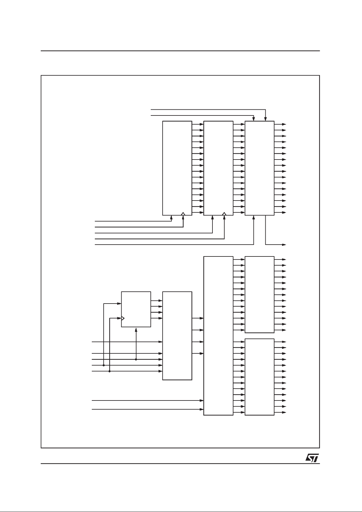
Figure 1. Block Diagram
LINES
&
PRINT HEAD
DRIVER
POWER
LOGICAL
SUPPLIES
CONTROL
PQFP100
In order to avoid output activation during the supply transient, an internal power-up system is implemented.
As supporting function, L6452is capable of sensing the head silicon temperature and to electrically check each nozzle.
The device is also integrating a thermal protection.
16 POWER LINES
13 ADDRESS LINES
CHANNEL A
PRINT HEAD
A
A/D & PRINT HEAD
TEMPERATURE
CONTROL LINES
March 1999
PRINT HEAD
TEMPERATURE
CONTROL
13 ADDRESS LINES
CHANNEL B
ANALOG
INPUTS
PRINT HEAD
B
D97IN523
1/16
L6452
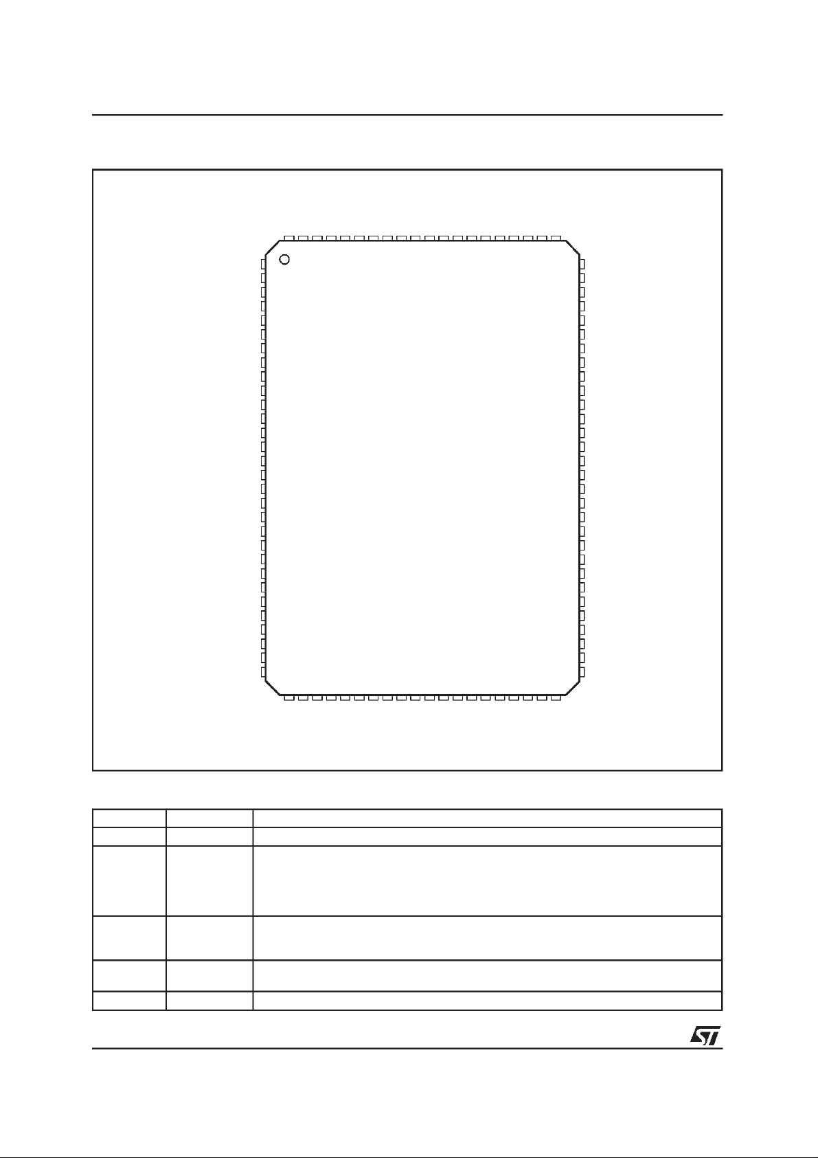
PIN CONNECTION (Topview)
RXA
RXB
VXa
VXb
_ONENABLE
CRCLOCK
CRDATA
96
97
98
99
100
V
C
V
C
V
C
V
C
V
C
C
V
C
V
C
1
2
3
4
5
6
7
8
9
10
12
13
14
15
16OUTPUT7
17
18
19
20V
21
22
23
24
25OUTPUT1
26
27
28
29
30NCEN
31 32 33 34 35
SDI
LATCH_DATA
SDC
LONG_PULSE
SHORT_PULSE
CRLATCH
OUTPUT15
POWGND
OUTPUT14
OUTPUT13
OUTPUT12
OUTPUT11
OUTPUT10
OUTPUT9
OUTPUT8
POWGND
OUTPUT6
OUTPUT5
OUTPUT4
OUTPUT3 59
OUTPUT2
POWGND
OUTPUT0
LATCH_CLEAR
REXT
95 94 93 92 9091 89 88 87 86 85
361137 38 39 40 41
ADCK
_RESET
CONV_START
CS_GND
NCOUT
CH0_BUF
aVDD
V
VSTEP-UP
42 43 44
ADDATA
ANALOGND
STEPUP_BO
STEPUP_GND
CLKCS0
_ENCH
45 46 47 48 49 50
a
V
CH5
VREF
ADCGND
RESCS1
84 83 8182
CH4
UPC52
S3
CH3
CH2
CHSEL
80
79
78
77
76
75
74
73
72
71
70
69
68
67
66
65
64
63
62
61
60
58
57
56
55
54
53
52
51
CH1
ENLC
GND
HSA1
HSA2
HSA3
HSA4
HSA5
HSA6
HSA7
HSA8
HSA9
HSA10
HSA11
HSA12
HSA13
V
HSB13
HSB12
HSB11
HSB10
HSB9
HSB8
HSB7
HSB6
HSB5
HSB4
HSB3
HSB2
HSB1
GND
D97IN489B
r
PIN FUNCTIONS
Pin # Name Function
1 CRlatch A rising edge latches the informationpresent intothe control register
2, 5, 6, 8, 9,
11, 12, 14,
16, 18, 19,
21, 22, 24,
25, 28
3, 7, 10, 13,
17, 20, 23,
26
4, 15, 27,
51, 79, 92
29 Latch Clear A high level resets all bit in thelatch
2/16
Output 15...0 Highside DMOS outputs. To be active, Short Pulse and/or Long Pulse and Nozzle
Check Enable must have a low level
Vc Outputs Power Supply
GND logicand power ground
PIN FUNCTIONS (continued)
Pin # Name Function
30 NCEn A high level enables the internal current sourcesand disables all DMOS outputs.To
be active, the internal current sources must have their corrsponding bit set inthe 16 bit
latchand Long Pulse must be set to low level. A low level enables the internalHSA/B
shortcircuit detection
31 Latch Data A rising edge latches the 16 bit stored in the shift register in the 16 bit latch
32 SDI Serialdata input of the shift register
33 SDC The data bit presented to the Serial Data Input pin is stored intothe register on the
risingedge of this pin
34 Long Pulse Alow level activates all outputs having their coresponding bit in the 16 bit latch set
(thispin has an internal pull-up resistor)
35 Short Pulse A low level activates all outputs having their coresponding bit in the 16 bit latch reset
(thispin has an internal pull-up resistor)
36 _Reset A low level disables all functions and clears all registers
37 ConvStart A high level enables the A/D to start the new conversion
38 ADCK A/D clock signal; the ADDATA signal are valid on the falling edge of this pin
39 NCOut If Nozzle Check Enable is high this output provides a high level when the open load is
detected on the output. If Nozzle Check Enable is lowthis output provides a highlevel
when a short circuit is detected on HSA/B output
40 CH0_buf Analogoutput signal (CH0 buffered)
41 ADDATA A/D serial data output
42 AnalogGND Analog ground connection
43 ADCGND Groundof internal ADC
44, 90 Va Power supply
45 Vref Reference voltage generator
46 to 50 CH5..CH1 A/D input signals
52 to 64 HSB1..HSB13 Head selector address output channel B
65 Vr Head Select Power Supply
66 to 78 HSA13..HSA1 Head selector address output channel A
80 EnlC A high level enables the counter and the internaldecoder will activate of the HSx
outputsaccording to the counter’s outputs. Signal S0 becomes Clock Counter and S1
becomes Reset Counter
81 ChSel A low level enables channel A and a high level enables channel B
82 S3 Decoder input signals when Enable Counter is low
83 UpC/ S2 A high level enables the internalcounter to up counting. A low level enables down
counting
84 ResC/S1 A low level resets the internal counter
85 _EnCh A low level enables the selected channel (this input has an internal pull up resistor)
86 ClkC/S0 Ahighlevel clocks the internal counter
87 Step up GND Groundof step up block
88 Step up boost Boostvoltage
89 Vstep up Driving voltage of power DMOS stage
91 VDD 5V logic supply
93 Rext An external resistor connected versus ground fixes the internal current source value
94, 95 RxB, RxA Current source outputs
96, 97 VxA, VxB RxA, RxB voltage after an optional external filter
98 _ONenable Alowlevel enables the current source generator according the _A/B and ON/_OFF
control register bit
99 CRclock Data on pin CRdata are stored into the register on the rising edge of this pin
100 CRdata Control register serial data input
L6452
3/16
L6452
Figure 2. Block Diagram: Nozzle activationpart.
* LONGPULSE
* SHORTPULSE
16 BIT
INPUT
PARALLEL
OUTPUT
SERIAL DATA INPUT
SERIAL DATA CLOCK
LATCH CLEAR
LATCH DATA
NOZZLE CHECK ENABLE
SERIAL
&
16 BIT LATCH
16
POWER
OUTPUT
STAGES
OUTPUT 0
OUTPUT 1
OUTPUT 2
OUTPUT 3
OUTPUT 4
OUTPUT 5
OUTPUT 6
OUTPUT 7
OUTPUT 8
OUTPUT 9
OUTPUT 10
OUTPUT 11
OUTPUT 12
OUTPUT 13
OUTPUT 14
OUTPUT 15
NOZZLE
OUTPUT
CHECK
INTERNAL
ENABLE
COUNTER
SEL 3
UP COUNTING/SEL 2
*RESET COUNTER/SEL1
CLOCK COUNTER/SEL 0
*SELECT CHANNEL
*ENABLE CHANNEL
0to
13
UP/DOWN
COUNTER
SELECTOR
D97IN524
HSA 1
HSA 2
HSA 3
HSA 4
HSA 5
13
MOS
DRIVERS
CHANNEL A
C0
C1
4to13
LINES
DECODER
C2
C3
13
MOS
DRIVERS
CHANNEL B
HSA 6
HSA 7
HSA 8
HSA 9
HSA 10
HSA 11
HSA 12
HSA 13
HSB 1
HSB 2
HSB 3
HSB 4
HSB 5
HSB 6
HSB 7
HSB 8
HSB 9
HSB 10
HSB 11
HSB 12
HSB 13
4/16

Figure 3. Block Diagram: Power Line Output Stage.
DATA BIT 0
1
0
L6452
POWER SUPPLY
10mA
OUTPUT 0
FROM 16 BIT
DATA LATCH
DATA BIT 1
DATA BIT 15
*LONG PULSE
* SHORT PULSE
NOZZLE CHECK ENABLE
D97IN525
OUTPUT 1
OUTPUT 15
TRIGGER
NOZZLE CHECK OUTPUT
5/16
 Loading...