

L6450
28 CHANNEL INK JET DRIVER
ADVANCE DATA
40VDMOS OUTPUTBREAKDOWN
TWODECODER OPTIONSARE INCLUDED
PRECISEOUTPUTENERGY
ESD OUTPUT PROTECTION WITH CLAMP-
ING DIODES
VERYLOW QUIESCENTCURRENT
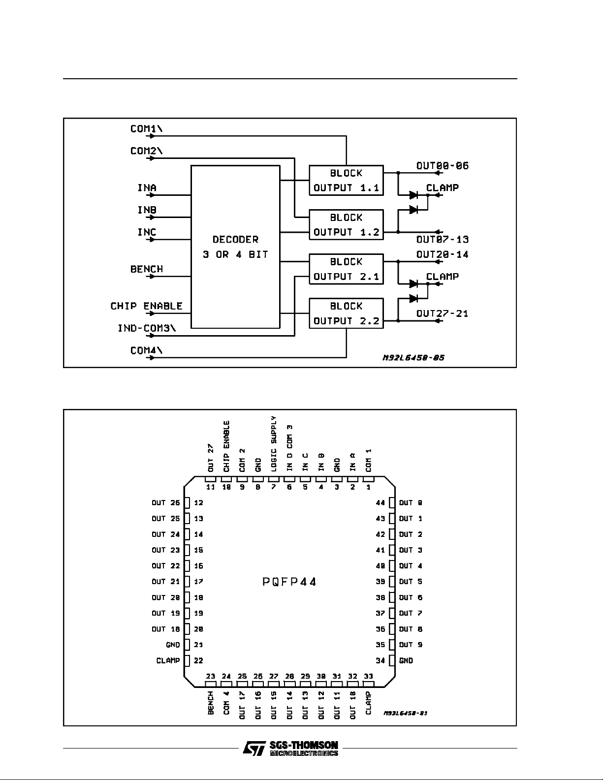
PLCC44 OR PQFP44(10 x 10mm)
DESCRIPTION
The L6450 is realized in Multipower BCD Technology which combines isolated DMOS power
transistors with CMOS and Bipolar circuits on the
same IC. By using mixed technology it has been
possible to optimize the logic circuitry and the
powerstage to achieve the best possible performances.
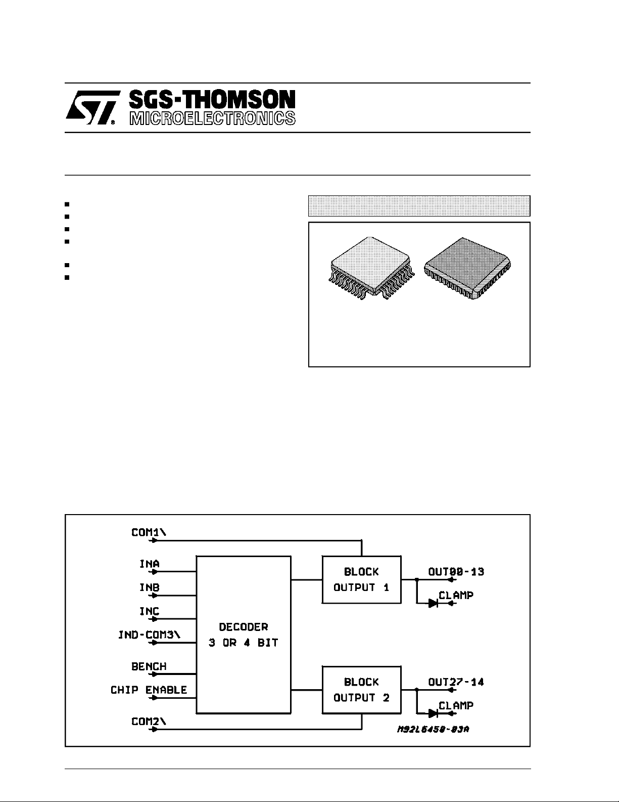
Intended to be used in ink jet Printer Applications
as 4 to 28 (2 x 14) or 3 to 28 (4 x 7) lines selectable decoder/driver, the L6450 device driver has
the advantages of low power CMOS inputs and
logic, with 28 high current and high voltage
DMOS outputs capable of sustaining a maximum
of 40V.
On systempower up the output drivers are locked
out using the chip enable function; four enable in-
MULTIPOWER BCD TECHNOLOGY
PQFP44 PLCC44
puts are available for the differentdriver banks.
An internal power-on system is implemented in
order to avoid wrong output commutation during
the supply voltage transients.
Using a mask option during manufacturing allows
a differentdecoding.
Control of the energy delivered to the print head
ismade by means of a specialcircuitry.
All driver outputs are capable of withdstanding a
contactdischargeof ±8KV with the IC biased.
BLOCK DIAGRAM (case of 4 bit)
March 1994
This is advanced information on a new product now in developmentor undergoing evaluation. Details are subjectto change without notice.
1/9
L6450
BLOCK DIAGRAM (case of 3 bit)
PQFP44PIN CONNECTION (Top view)
2/9
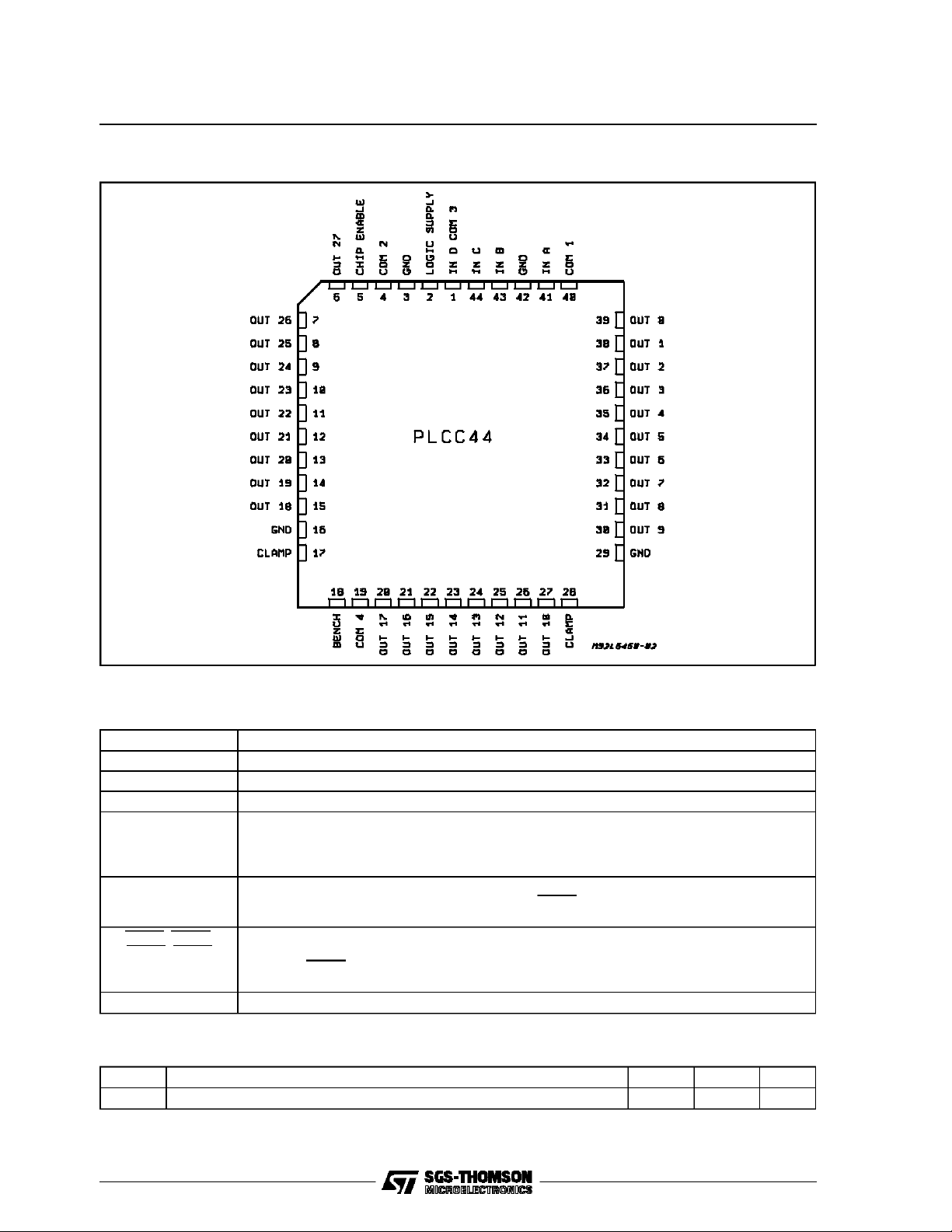
PLCC44PIN CONNECTION (Top view)
L6450
PIN FUNCTIONS
Name Function
V
DD
GND Logic and Power Ground.
OUT0 to OUT27 DMOS Outputs.
CLAMP This pins have to be connected to the power supply voltage of the head resistors, each of the
INA, INB, INC, IND Decoder inputs.
COM1, COM2,
COM3, COM4
CHIP ENABLE A logic high enable the chip.
5V Logic Supply.
output DMOS have their drain connected with the anode of a protection diode, all the catodes
of the protection diodes are collected to the pins clamp. If the CLAMP pins are not connected
to the power, the deviceis not supplied.
The input IND shares the pin with the other input COM3, the two different functions are
selected by the pin Bench.
A low logic input on this pins enable the outputs selected by the decoderinputs according to
the logic level of the pin bench.
The input COM3 shares the pin with the other input IND, the two different functionsare
selected by the pin Bench.
THERMAL DATA
Symbol Parameter PQFP44 PLCC44 Unit
R
th j-amb
(*) device mountedon PCB.
Thermal Resistance Junction-Ambient Max. 55 (*) 65 (*) °C/W
3/9
 Loading...