

0.5A INDUSTRIAL INTELLIGENT POWER SWITCH
■
0.5A OUTPUT CURRENT
■ 8V TO 35V SUPPLY VOLTAGE RANGE
■
NON DISSIPATIVE SHORT CIRCUIT
PROTECTION
■ THERMAL SHUTDOWN
■
OPEN GROUND PROTECTION
■
NEGATIVE VOLTAGE CLAMPING FOR FAST
DEMAGNETIZATION
■ UNDERVOLTAGE LOCKOUT WITH
HYSTERESIS
■
OPEN LOAD DETECTION
■ TWO DIAGNOSTIC OUTPUTS
■
OUTPUT STATUS LED DRIVER
■
IMMUNITY AGAINST BURST TRANSIENT
(IEC 801-4), see application schematic.
■
ESD PROTECTION (HUMAN BODYMODEL
±2KV)
L6375
PRELIMINARY DATA
MULTIPOWERBCD TECHNOLOGY
SO20 MINIDIP
ORDERING NUMBERS:
L6375D L6375
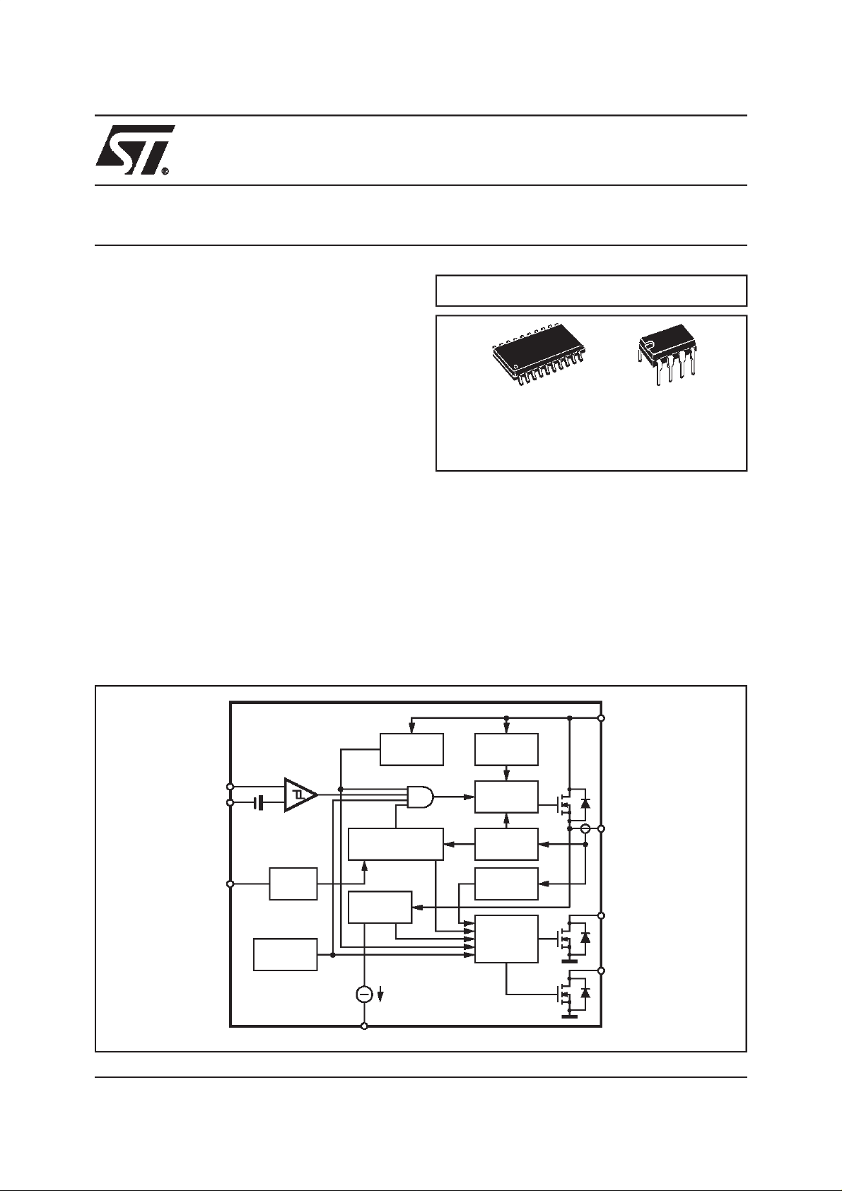
DESCRIPTION
The L6375 is a monolithic fully protected, full diagnostic 0.5A Intelligent Power Switch. it is designed to
drive any kind of R-L-C load with controlled output
voltage slew rate and non dissipative short circuit
protection. An internal Clamping Diode enables the
fast demagnetization of inductive loads. Diagnostic
for CPU feedbackand extensive use of electrical protections make this device extremely rugged and specially suitable for industrial automation applications.
BLOCK DIAGRAM
V
S
UNDER
VOLTAGE
INPUT
1.4V
OSC
THERMAL
PROTECTION
+
-
NON DISSIPATIVE
SHORT CIRCUIT
OUTSTATUS
3mA
OUTPUT STATUS
IN+
IN-
Con
February 2000
This ispreliminary information ona new product now in development or undergoing evaluation. Details are subject to change without notice.
CHARGE
PUMP
DRIVER
CURRENT
LIMITATION
OPEN LOAD
DETECTION
DIAGNOSTIC
OUT
DIAG1
DIAG2
D95IN208B
1/12
L6375
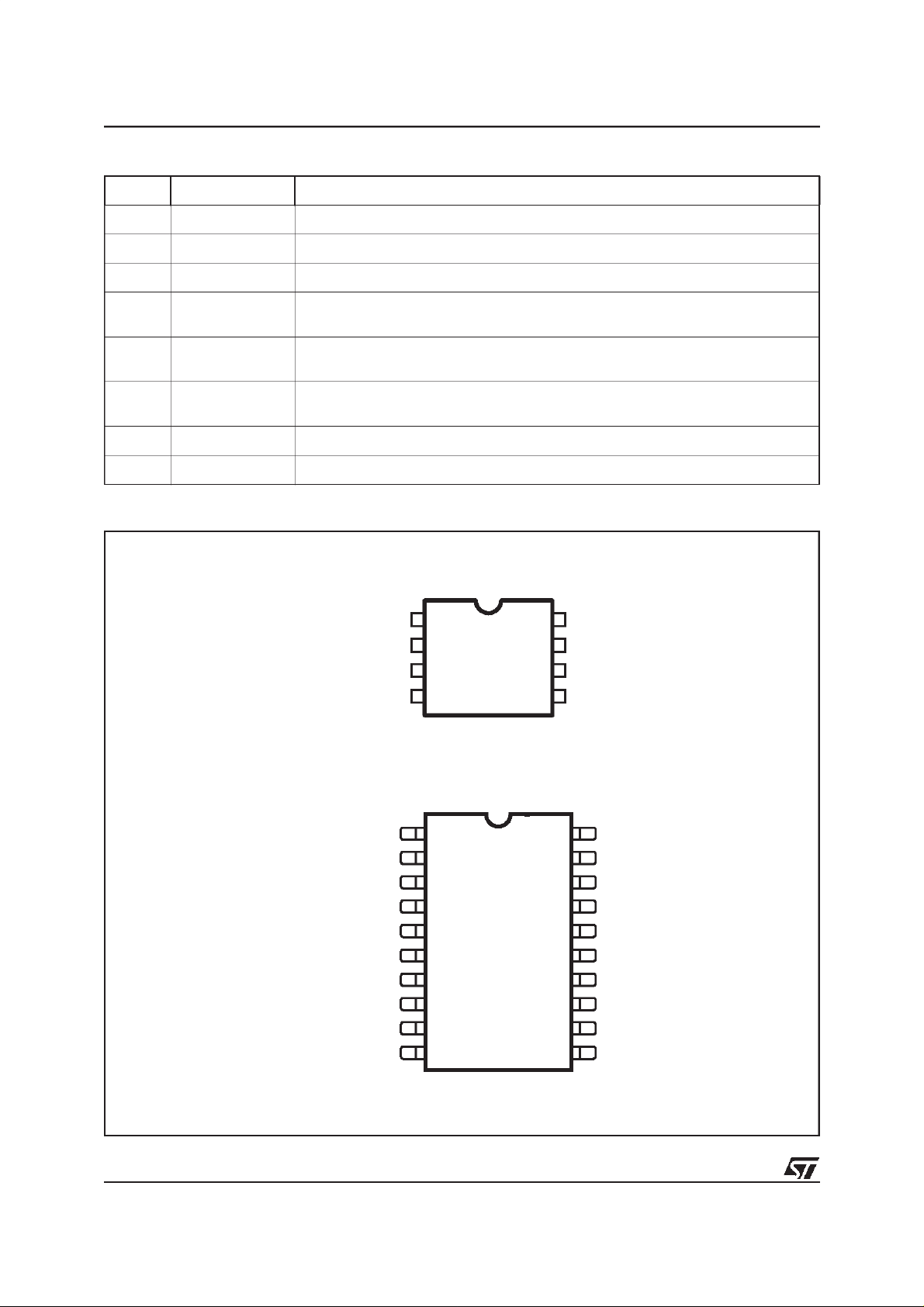
PIN FUNCTION (Pin numbering referred to Minidip package)
N° Pin Description
1 GND Ground
2 OUT High side output. Controlled output with current limitation
3 Vs Supply voltage input. Range with under voltage monitoring
4 OUTPUT STATUS Led driver to signal thestatus of the output pin. The pin is active ( sources current )
5 DIAG1 Diagnostic 1 output. This open drain reports the IC working conditions. (See
6 DIAG2 Diagnostic 2 output. This open drain reports the IC working conditions. (See
7 IN+ Comparator non inverting input
8 ON DELAY Delay setting for overcurrent diagnostic
when the outputis considered high. (See fig. 1)
Diagnostic truth table)
Diagnostic truth table)
PIN CONNECTION (Top view)
GND
OUTPUT
V
OUTPUT STATUS
1
2
MINIDIP
3
S
4 DIAG2
ON DELAY8
INPUT +
7
DIAG1
6
5
2/12
N.C.
GND
N.C.
OUTPUT
N.C.
V
S
N.C.
N.C.
N.C. N.C.
OUTPUT STATUS N.C.
2
3
4
5
6
7
8
9
10
SO20
20
19
18
17
16
15
14
13
12
11
N.C.1
ON DELAY
N.C.
INPUT+
N.C.
DIAG1
DIAG2
N.C.
L6375
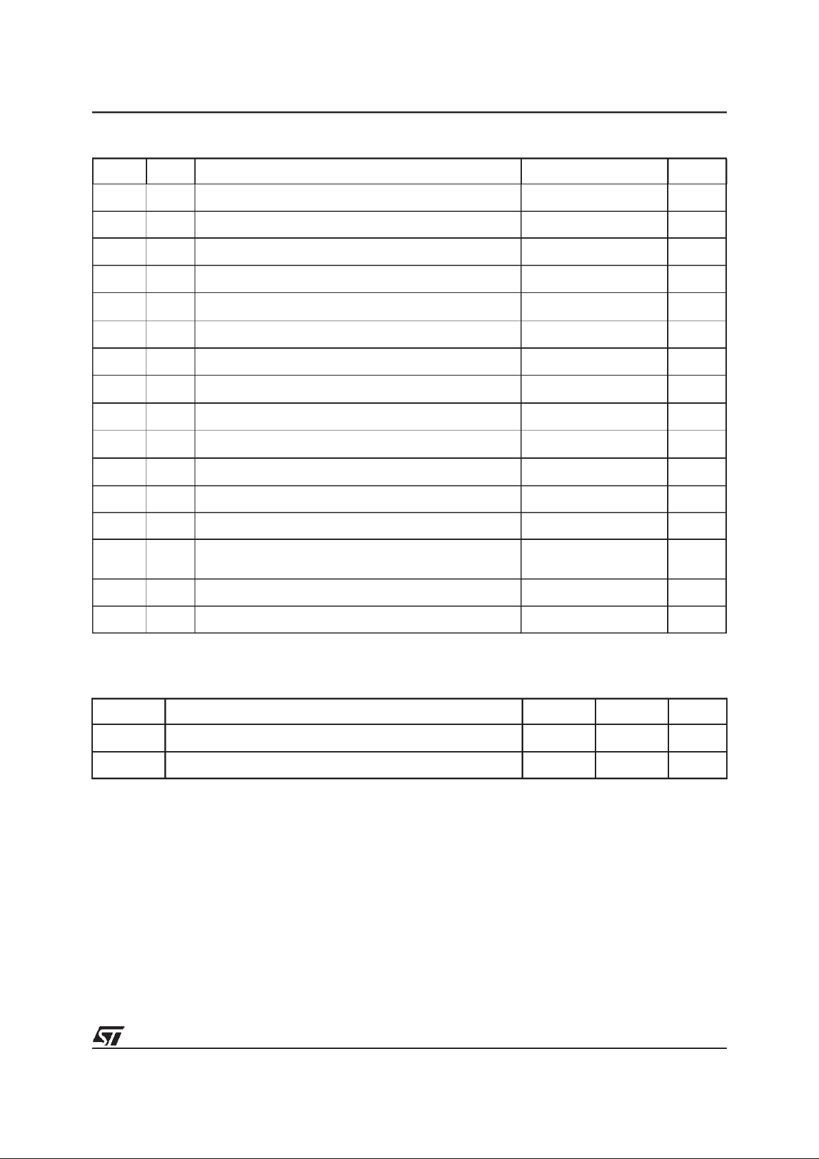
ABSOLUTEMAXIMUM RATINGS
Symbol Pin Parameter Value Unit
V
s
V
s
Vs -Vout
Vod
od
I
Iout
Vout
Ptot
diag
V
diag
I
Ii
V
i
T
op
3 Supply Voltage (tw < 10 ms) 50 V
3 Supply Voltage (DC) 40 V
3 vs 2 Supply to Output Differential voltage internally limited
5 Externally Forced Voltage -0.3 to 7 V
5 Externally Forced Current ±1mA
2 Output Current (see also Isc) internally limited
2 Output Voltage internally limited V
Power Dissipation internally limited
5.6 External voltage -0.3 to 40 V
5.6 Externally forced current -10 to 10 mA
7 Input Current 20 mA
7 Input Voltage -10 to Vs+0.3 V
Ambient temperature, operating range -25 to 85 °C
(Pin numbering referred to Minidip package)
T
Tstg
E
j
I
Junction temperature, operating range
(see Overtemperature Protection)
Storage temperature -55 to 150 °C
Energy Induct. Load TJ=85°C 200 mJ
-25 to 125 °C
THERMAL DATA
Symbol Parameter Minidip SO20 Unit
R
th j-case
R
th j-amb
Thermal Resistance Junction to Case Max. °C/W
Thermal Resistance Junction to Ambient Max. 100 90 °C/W
3/12

L6375
ELECTRICAL CHARACTERISTCS
(VS=24V;Tj= –25 to +125°C, unless otherwise specified; pin numbering referred to Minidip package)
Symbol Pin Parameter Test Condition Min. Typ. Max. Unit
smin
V
V
Vsth1
Vsth2
Vshys
I
Iqo
Vith
V
iths
Vil
Vih
V
Iib
Idch
3 Supply Voltage for Valid
Diagnostic
3 Operative Supply Voltage 8 24 35 V
s
3 Undervoltage Threshold 1 (See fig. 2) 7 7.5 8 V
3 Undervoltage Threshold 2 (See fig. 2) 6.5 7 7.5 V
3 Under Voltage Hysteresis 300 500 700 mV
3 Quiescent Current Output Open 800 µA
q
3 Quiescent Current Output On 1.6 mA
7 Input Threshold Voltage 0.8 1.3 2 V
7 Input Threshold Hysteresis 50 400 mV
7 Input Low Level Voltage -7 0.8 V
7 Input High LevelVoltage Vs< 18V 2 V
7 Input High LevelVoltage Vs> 18V 2 15 V
ih
7 Input Bias Current Vi= -7 to 15V -250 250
5 Delay Capacitor Charging
Current
diag
I
= >0.5mA;V
ON DELAYpin shorted to
Ground
diag = 1.5V;
435V
s -3 V
A
µ
2.5 µA
Vdon
Iolk
Vol
cl
V
Isc
old
I
Voth1
Voth2
Vohys
Iosd
Output Voltage Drop
2 Output Leakage Current Vi= LOW; V
2 Output Low State Voltage Vi = HIGH; pin floating 0.8 1.5 V
2 Internal Voltage Clamp (Vs-V
2 Short Circuit Output Current
2 Open Load Detection Current Vi=Vih;T
5.6 Output Status Threshold 1
Voltage
5.6 Output Status Threshold 2
Voltage
5.6 Output Status Threshold
Hysteresis
5.6 Output Status Source Current V
I
= 500mA Tj=25°C
out
= 125°C
T
j
I
= 625mA T
out
= 125°C
T
j
)
o = 200mA
I
out
single pulsed =300µs
= 8 to 35V; Rl=2
V
s
(See fig. 1) 4.5 5 5.5 V
(See fig. 1) 4 4.5 5 V
(See fig. 1) 300 500 700 mV
out >Voth1 ;Vos = 2.5V 24mA
=25°C
j
=0 100 µA
out
48 53 58 V
Ω;
= 0 to +85°C136mA
amb
0.75 1.1 1.5 A
200
320
250
400
280
440
350
550
mV
mV
mV
mV
4/12
 Loading...