

SGS Thomson Microelectronics L6370L, L6370D Datasheet
L6370
2.5A HIGH-SIDE DRIVER
INDUSTRIALINTELLIGENT POWER SWITCH
2.5A OUTPUT CURRENT
9.5V TO35V SUPPLY VOLTAGE RANGE
INTERNALCURRENT LIMITING
THERMALSHUTDOWN
OPENGROUNDPROTECTION
INTERNALNEGATIVE VOLTAGE CLAMPING
TOV
- 50VFOR FAST DEMAGNETIZATION
S
DIFFERENTIAL INPUTS WITH LARGE COMMON MODE RANGE AND THRESHOLD
HYSTERESIS
UNDERVOLTAGELOCKOUTWITHHYST ERESIS
OPENLOAD DETECTION
TWODIAGNOSTICOUTPUT S
OUTPUTSTATUS LEDDRIVER
NON DISSIPATIVE SHORT CIRCUIT PRO-
TECTION
PROTECTIONAGAINST AND SURGE TRAN-
SIENT (IEC 801-5)
IMMUNITY AGAINST BURST TRANSIENT
(IEC801-4)
ESD PROTECTION (HUMAN BODY MODEL
2KV)
±
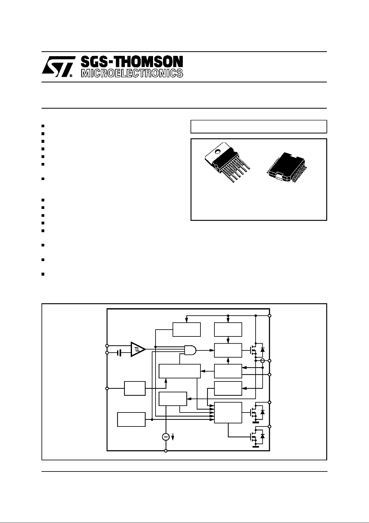
BLOCK DIAGRAM
MULTIPOWER BCD TECHNOLOGY
MULTIWATT11(in line)
ORDERINGNUMBERS: L6370L (MULTIWATT11)
PowerSO20
L6370D (PowerSO20)
DESCRIPTION
The L6370 is a monolithic Intelligent Power
Switch in Multipower BCD Technology, for driving
inductive or resistive loads. An internal Clamping
Diode enables the fast demagnetizationof inductive loads. Diagnostic for CPU feedback and extensive use of electricalprotections make this device extremely rugged and specially suitable for
industrialautomation applications.
March 1997
IN+
IN-
ON-DELAY
INPUT
1.4V
OSC
THERMAL
PROTECTION
+
-
NON DISSIPATIVE
SHORT CIRCUIT
OUTSTATUS
3mA
OUTPUT STATUS
UNDER
VOLTAGE
CHARGE
PUMP
DRIVER
CURRENT
LIMITATION
OPEN LOAD
DETECTION
DIAGNOSTIC
D95IN208D
V
S
OUT
RSC
DIAG1
DIAG2
1/10
L6370
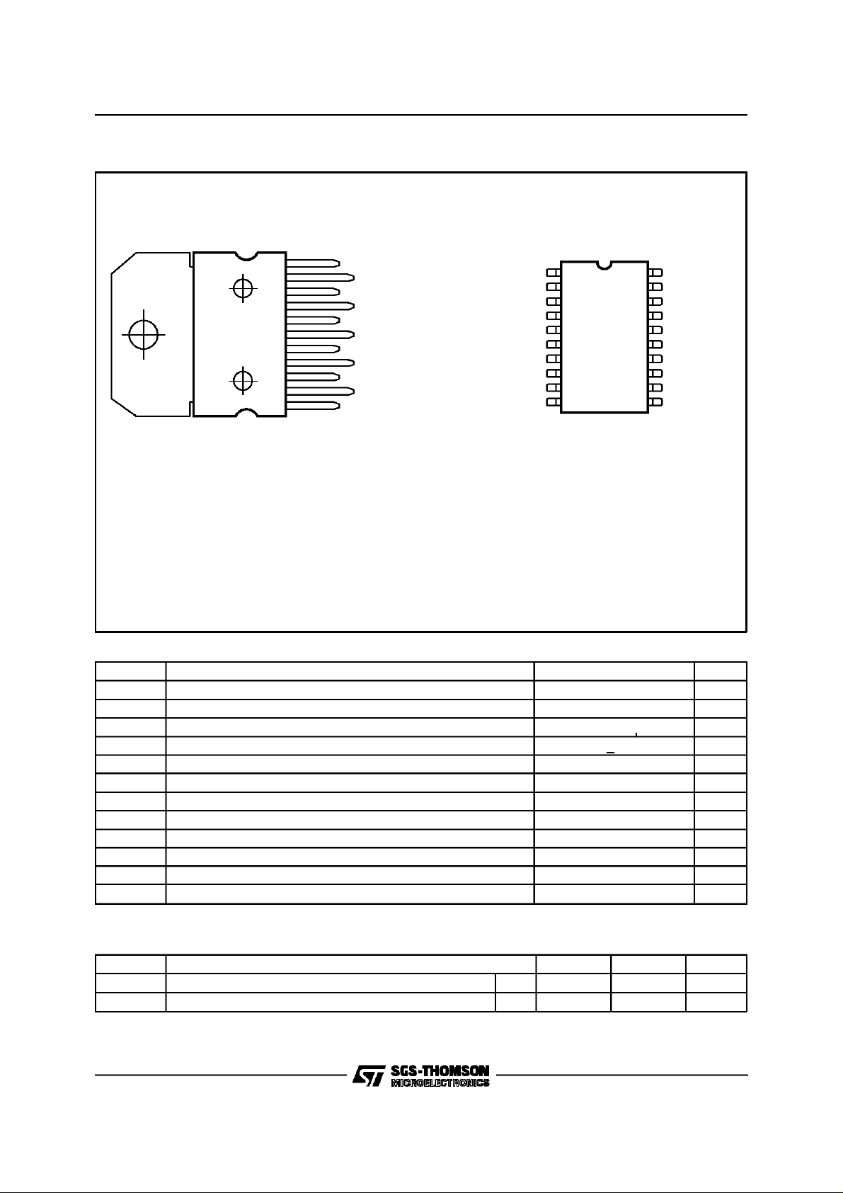
PIN CONNECTION (Topview)
11
10
9
8
7
6
5
4
3
2
1
D95IN209A
OUTPUT
SUPPLY VOLTAGE
OUTPUT
RSC
ON-DELAY
GND
OUTPUT STATUS
INPUT INPUT +
DIAGNOSTIC 2
DIAGNOSTIC 1
GND
OUTPUT
OUTPUT
ON-DELAY
SUPPLY VOLTAGE
N.C.
OUTPUT
OUTPUT N.C.
GND GND
2
3
4
5
6
7
8
9
10
20
19
18
17
16
15
14
13
12
11
GND1
OUTPUT STATUS
INPUT INPUT +
N.C.SUPPLY VOLTAGE
DIAGNOSTIC 2
DIAGNOSTIC 1
RSC
D95IN210B
Note: Outputpins must be must be connected externally to the package touse all leadsfor the outputcurrent(Pin9 and11 for Multiwatt
package, Pin 2, 3, 8 and 9 for PowerSO20 package).
ABSOLUTE MAXIMUM RATINGS (Pinnumberingreferredto Multiwatt package)
Symbol Parameter Value Unit
V
V
S–VO
V
I
V
V
I
P
T
T
E
S
od
od
I
O
tot
op
stg
Supply Voltage (Pin 10) (TW< 10ms) 50 V
Supplyto Output Differential Voltage.Seealso VCl(Pins10 - 9) internally limited V
Externally Forced Voltage (Pin7) -0.3 to 7 V
Externally Forced Voltage (Pin7) +1 mA
Input Voltage (Pins 3/4) -10 to VS +10 V
i
Differential Input Voltage (Pins 3 - 4) 43 V
i
Input Current (Pins 3/4) 20 mA
i
Output Current (Pin 9). See also ISC (Pin 9) internally limited A
Power Dissipation.See also THERMAL CHARACTERISTICS. internally limited W
Operating Temperature Range (T
) -25 to +85 °C
amb
Storage Temperature -55 to 150 °C
Energy Induct.Load TJ=85°C1J
I
THERMAL DATA
Symbol Description Multiwatt PowerSO20 Unit
Thermal Resistance Junction-case Max. 1.5 1.5 °C/W
Thermal Resistance Junction-ambient Max. 35 – °C/W
2/10
R
th j-case
R
th j-amb

PIN FUNCTION (pinnumbering referred to Multiwattpackage)
N. Name Function
1 DIAG1 DIAGNOSTIC 1 output. This open drain reports the IC workingconditions. (See
Diagnostic truth table)
2 DIAG1 DIAGNOSTIC 2 output. This open drain reports the IC workingconditions. (See
Diagnostic truth table)
3 IN - Comparator non inverting input
4 IN+ Comparator inverting input
5 OUTSTATUS This current source output is capable of drivinga LED to signal the status of the output
pin. The pin is active (source current) when the output pin is considered high (See fig 1)
6 GND Ground
7 ON-DELAY Programmable ON time interval duration during short circuit operation
8 RSC Current limitation setting.
9 OUTPUT High Side output with built-in current limitation
10 V
S
Supply Volatge Input, the valueof the supplyvoltage is monitored to detect under voltage
condition
11 OUTPUT High Side output with built-in current limitation
ELECTRICALCHARACTERISTICS (VS= 24V; TJ= –25 to +125°C, unless otherwise specified)
Symbol Parameter Test Condition Min. Typ. Max. Unit
V
smin
V
s
I
q
V
sth1
V
sth2
V
shys
I
sc
V
don
I
oslk
V
ol
V
cl
I
old
V
id
I
ib
V
ith
V
iths
R
id
I
ilk
Supply Voltage for Valid
I
> 0.5mA ; V
diag
= 1.5V 4 35 V
dg1
Diagnostics
Supply Voltage (operative) 9.5 24 35 V
Quiescent Current
I
out=Ios
=0
V
V
il
ih
0.8
3
1.4
5
Undervoltage Threshold 1 (See fig. 1), Tamb = 0 to +85°C 8.5 9 9.5 V
Undervoltage Threshold 2 8 8.5 9 V
Supply Voltage Hysteresis 300 500 700 mV
Short Circuit Current VS= 9.5 to 35V; RL=2
Output Voltage Drop I
5kΩ <R
0<R
out
I
out
< 30kΩ
SC
<5kΩ 2.6 3.2 4 A
SC
= 2.0A Tj=25°C
T
= 125°C
j
= 2.5A Tj=25°C
T
= 125°C
j
Ω
(kΩ)A
15/R
SC
200
320
250
400
280
440
350
550
Output Leakage Current Vi=Vil;Vo= 0V 500 µA
Low State Out Voltage Vi=Vil;RL=∞ 0.8 1.5 V
Internal Voltage Clamp (VS-VO)IO=1A
48 53 58 V
Single Pulsed: Tp =300µs
Open Load Detection Current Vi=Vih;T
Common Mode Input Voltage
VS= 18 to 35V –7 15 V
= 0 to +85°C136mA
amb
Range (Operative)
Input Bias Current Vi= –7 to 15V; –In = 0V –250 250 µA
Input Threshold Voltage V+In > V–In 0.8 1.4 2 V
Input Threshold Hysteresis
V+In > V–In 50 400 mV
Voltage
Diff. Input Resistance 0 < +In < +16V; –In= 0V
–7 < +In < 0V ; –In = 0V
Input Offset Current V+In = V–In +Ii
0V < V
<5.5V –Ii
i
–In = GND +Ii
0V < V+In <5.5V –Ii –250
+In = GND +Ii
0V < V–In <5.5V –Ii
–20
–75 –25
–100
–50
400
150
+10
–125
–30
–15
+20 µA
+50
L6370
mA
mA
mV
mV
mV
mV
K
Ω
KΩ
A
µ
A
µ
µA
µA
µA
3/10
 Loading...