

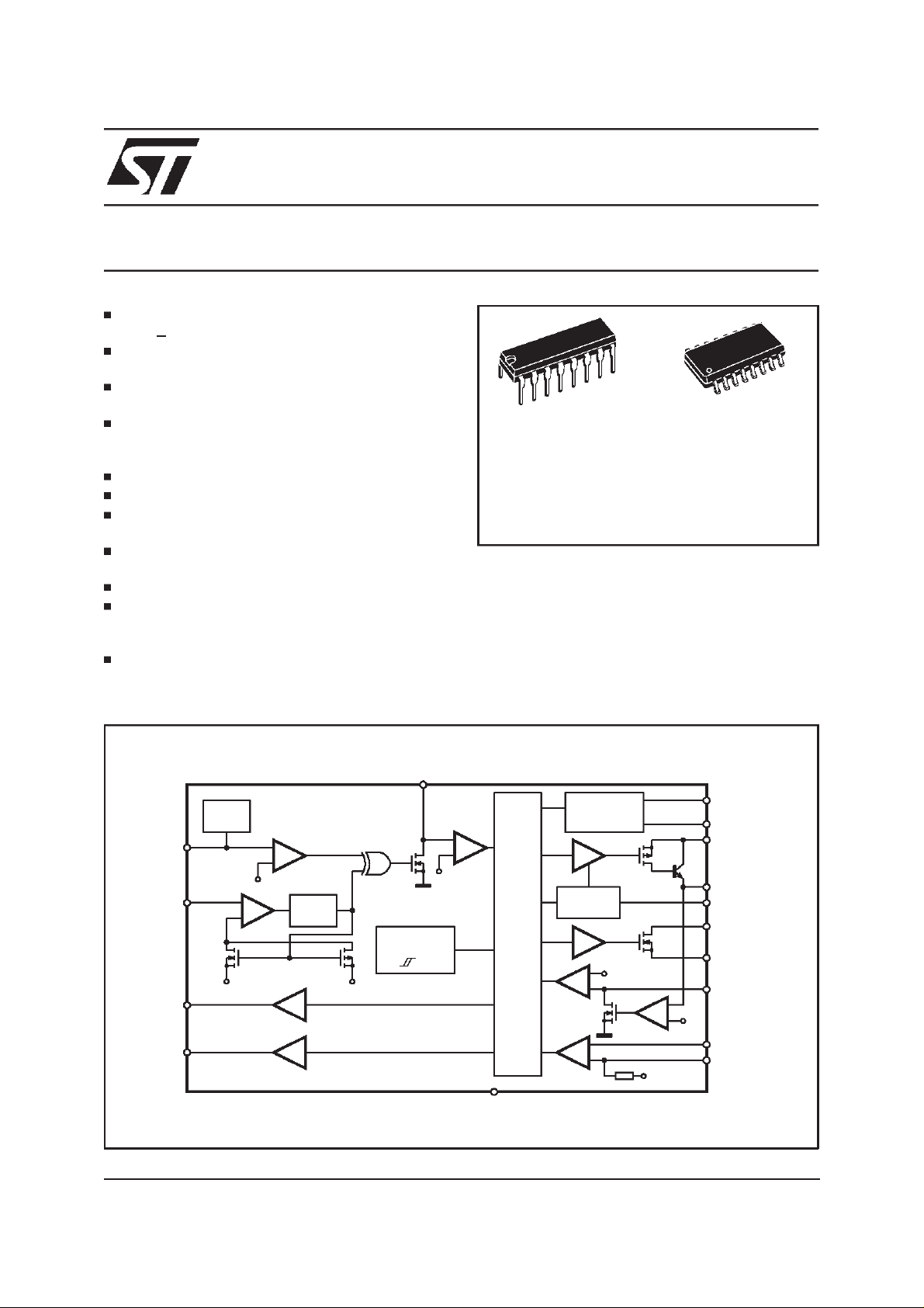
SMART DRIVER FOR POWER MOS & IGBT
PEAK HIGH OUTPUT CURRENT CAPABILITY(+8A)
WIDE SUPPLY VOLTAGE RANGE (12.5 TO
18V)
0 TO–7.5V NEGATIVE BIAS VOLTAGESUPPLY RANGE
OVER CURRENT AND DESATURATION
PROTECTION OF THE EXTERNAL POWER
DEVICE(EXTERNALLY PROGRAMMABLE)
LATCH-UPPROTECTION(FOR IGBT)
TWOSTEPS TURN-ON (PROGRAMMABLE)
PROTECTION AGAINST POSITIVE SUPPLY
UNDER-VOLTAGE
INPUT COMPATIBLE WITH OPTOCOUPLER
OR PULSETRANSFORMER
PROGRAMMABLETURN-ON DELAY
THERMAL PROTECTION WITH ON-CHIP
OVER-TEMPERATURE ALARM AND TURNOFF PROCEDURE
OPERATINGFREQUENCY UP TO 100kHz
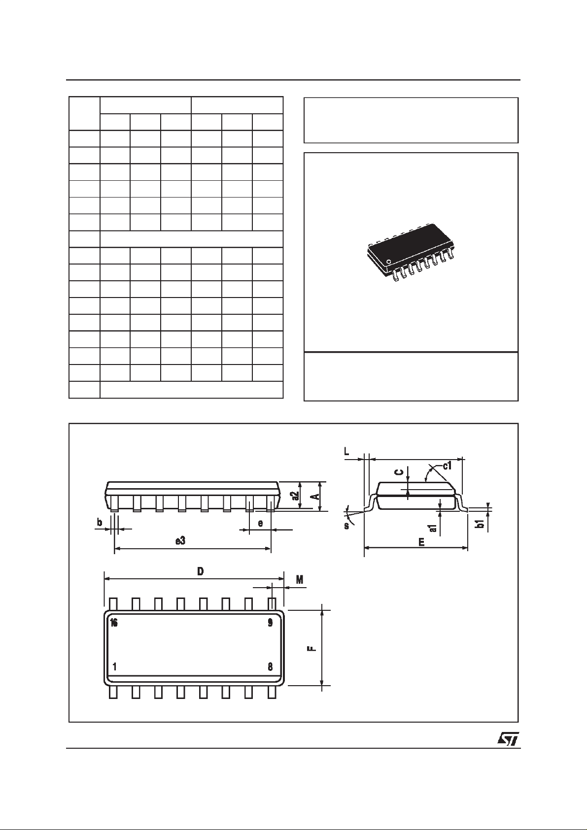
L6353
DIP16
ORDERING NUMBERS: L6353 (DIP)
DESCRIPTION
The L6353 device is a smart driver, with all the
driveandprotectionknow-how”on board”.
Available in both DIP and SO package, it can be
triggeredwitha logiclevelorwith the signalfroman
optocouplerora pulsetransformer.It filtersparasitic
inputsignalsand drives any MOSor IGBT.
SO16
L6353D (SO)
BLOCK DIAGRAM
2.5V
300µA
SELECT
INPUT
1.25V 3.75V
INV_OUT
ALARM
1.25V
+
−
DELAY
SUPPLY
UV SENSE
REFERENCES
3.15V
+
−
OUT1
CLAMPING
LOGIC
3.15V
−
+
−
+
+
−
7.5V
COM
D94IN106B
+
−
FILTER
200ns
THERMAL
SHUTDOWN
4V
V
CC
REF
V
POS
OUT1
CLAMP_PROG
OUT2
V
SS
MON_DELAY
ON_SENSE
ON_LEV_PROG
February 2000
1/11
L6353
DESCRIPTION (continued)
It monitors theon-state voltage drop of thedriven
power device and protectsit againstoverload and
short circuit.
The on-state voltage drop level is externallyprogrammable from 5 to 15V. This function is inhibited during the turn-on of the external power device for an externally programmableperiod.
An internal inhibition time of 200ns avoids false
triggering.
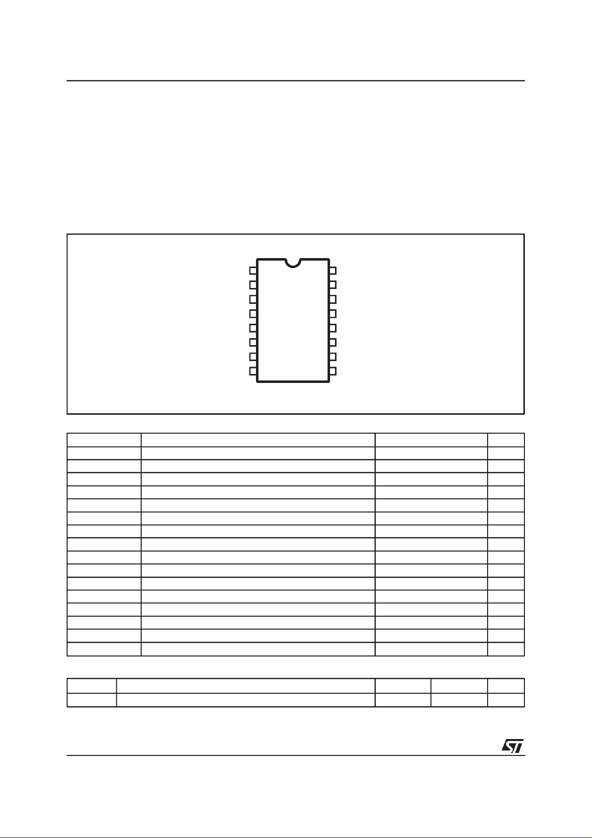
PIN CONNECTION (topview)
OUT1
V
CC
V
POS
CLAMP_PROG
INV_OUT
ALARM
MON_DELAY
VREF
1
2
3
4
5
6
7
8 INPUT9
D94IN113A
Overload or overheating are signalled on an
alarmoutput. If temperature continuestoincrease
the power output is switched off and maintained
in the off-state until the temperature decreases
below the low threshold. A programmable turn-on
delay avoids cross conduction in bridge configurations.
To preservethe externalpower device (especially
IGBT) from the risk of latch-up, the gate voltage
can be risen in two different steps (of which the
first is externally programmablefrom7 to 11V).
16
15
14
13
12
11
10
OUT2
COM
V
SS
ON_SENSE
ON_LEV_PROG
SELECT
DELAY
ABSOLUTE MAXIMUM RATINGS
Symbol Parameter Value Unit
V
CC
V
SS
V
POS-VOUT1
V
OUT2-VSS
V
EXT1
V
EXT2
I
DELAY
I
MON_DELAY
V
ON_SENSE
I
OUT1
I
OUT2
I
INV_OUT
I
ALARM
P
tot
T
amb
T
stg
Supply Voltage referred to COM pin 20 V
Negative Supply Voltage referred to COM pin – 8 to 0 V
Collector-Emitter Voltage of High Side NPN 25 V
Drain-Source Voltage of Low Side DMOS 25 V
Externally Forced Voltage (pin 9) -0.3 to V
CC
Externally Forced Voltage (pins 4,7,10, 11, 12) -0.3 to 7 V
Sink Current pin Delay 3 mA
Sink Current PinMon_Delay 3 mA
Voltage on ON_SENSE Pin VSS-0.3 to V
CC
Positive Output Current (tp ≤1ms) (peak) 8 A
Negative Output Current (tp ≤1ms) (peak) 8 A
Output Current in INV_OUT Pin ±20 mA
Output Current in ALARM Pin ±20 mA
Total Power Dissipation internally limited
Operating Temperature Range -25 to +85
Storage Temperature -50 to +150 °C
THERMAL DATA
Symbol Parameter DIP16 SO16 Unit
R
thj-ambient
Thermal Resistance Junction-ambient Max 80 90 °C/W
V
V
C
°
2/11
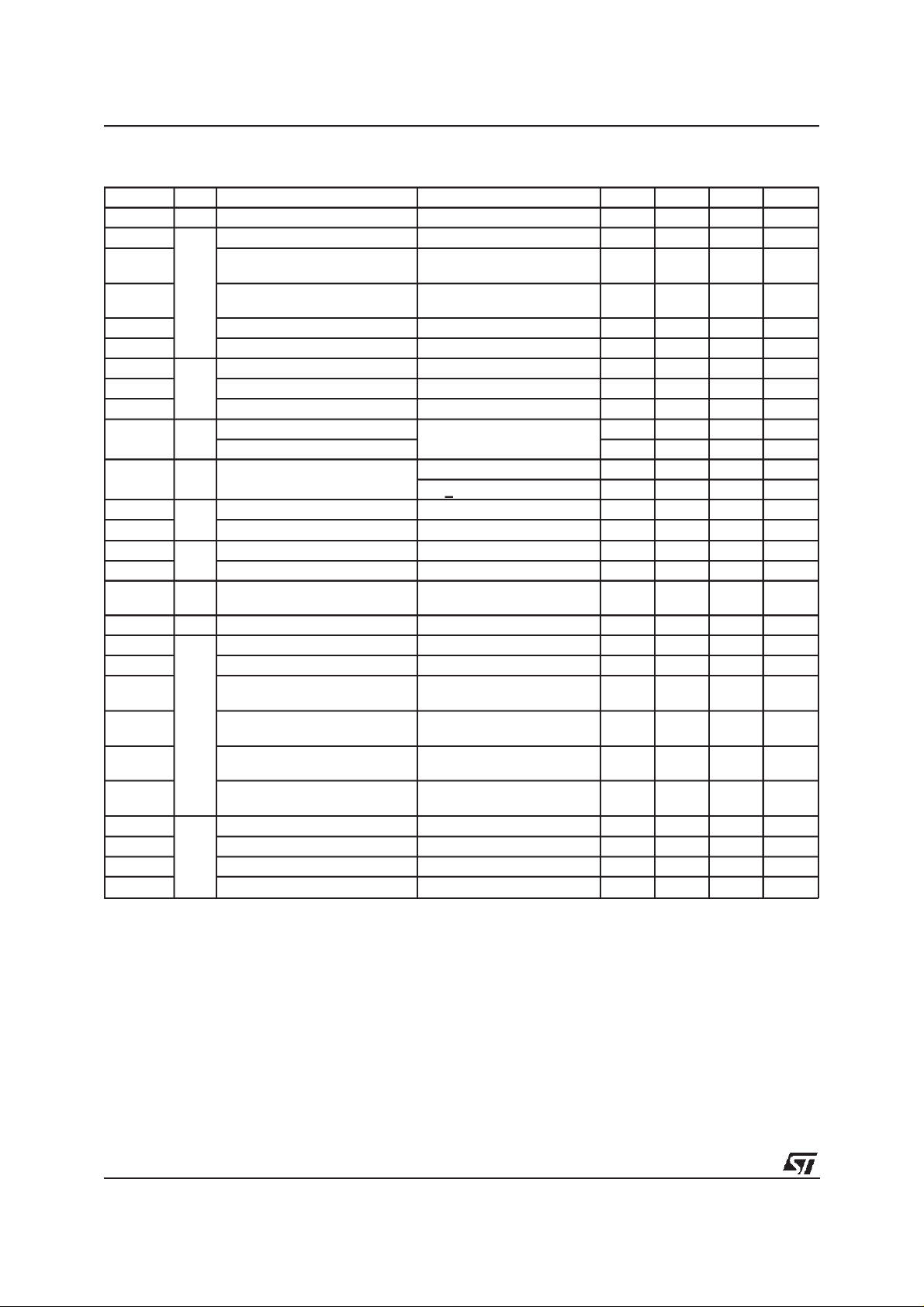
PIN FUNCTIONS
N. Name Function
1 OUT1 Output of high side driver (emitter of power NPN transistor).
2V
3V
CC
POS
4 CLAMP_PROG FirstStep of theGate Voltage Programming.
5 INV-OUT InvertedOutputDriverStatus.
6 ALARM Diagnostic OutputSignal. A fault condition is signalled by this output buffer.
7 MON_DELAY V
8V
REF
9 INPUT Input signal.
10 DELAY On Triggering Delay. An R-C network connected between this, the COM and the V
11 SELECT Select the direct/inverted mode in the Logic Level Mode. It’s also the reference pin in Pulse
12 ON_LEV_PROG V
13 ON_SENSE On State Monitor.
14 V
SS
15 COM Ground
16 OUT2 Output of the low side driver (drain of the DMOS).
Positive Supply Voltage (referred to COM).
See under voltage lockout functioning
Positive Bias Voltage (collector of theNPN power transistor).
The programming is achieved setting an appropriate voltageon this pin (i.e. usinga resistence
voltage divider).
Thebufferoutputis ableto drivesome auxiliary circuit(i.e. a LED).
Monitor Delay. An R-C network connected between this, the COM and the V
ON
define t
MON_DELAY
time interval(see fig 4)
REF
Output of the 5V/10mA internalvoltage reference.
The driving signal can be a logic level either active LOW (inverted mode) or HIGH (direct
mode) in the Logic Level or a pulse in the PulseTransformer Mode (see Figure 2)
definethe t
time interval(see fig 4)
DELAY
REF
transformer mode.
level programming.
ON
This pin is used to set the V
monitor level. The programming is achieved setting an
ON
appropriate voltage on this pin (i.e. using a resistive divider).
Thispin is used to monitor the turning on of the external power device.
Negative supply voltage (referred to the COM).
This pin is the source of the lowside driver DMOS.
L6353
pins,
pins,
3/11
L6353
DC ELECTRICAL CHARACTERISTICS (V
POS=VCC
=15V; VSS= -5 to 0V; Tj= -25 to +125°C; unless
otherwise specified)
Symbol Pin Parameter Test Condition Min. Typ. Max. Unit
V
V
V
CCth1
V
CCth2
V
CChys
I
CCq
V
drop_sig
V
R
V
R
I
V
R
V
t
V
V
V
V
V
drop
CC
V
I
so
I
si
dth
outs
SS
ON
V
I
in
inh
ton
toff
I
sl
sel
1V
POS-VOUT1
2 Operating Supply Voltage (referred to COM pin) 12.5 18 V
Under Voltage Upper
Threshold
Under Voltage Lower
Threshold
Under VoltageHysteresis 0.3 0.5 0.7 V
QuiescentSupply Current 5 mA
4, 12 Output Voltage pin floating 1.26 V
d
Sourced Current pin grounding 20 µA
Sinked Current pin at +5V -20
5, 6 High State Output Voltage Drop I
Low State Output Voltage Drop 3 V
ref
8 Output of Internal Voltage
Reference
7, 10 Comparator Input Resistance 100
in
Comparator Threshold 3.15 V
ins
13 Input Resistance 75 KΩ
Output Current pin grounded 200 µA
14 OperatingNegative Bias
Voltage
16 On Resistance OUT2 to VSS); I
il
ih
9 Low Level Voltage (Logic Level Mode) 0 1 V
High Level Voltage (Logic Level Mode) 4 V
Input Current 0<Vin<V
Inhibited Parasitic Pulse
Duration
Turn-on Threshold Voltage Referred to V
Turn-off Threshold Voltage Referred to Vsel
sl
sh
11 Low Level Voltage (Logic Level Mode) 0 1 V
High Level Voltage (Logic Level Mode) 2 V
Current Output of SELECT Pin Vsl= 0V (Logic Level Mode) 300 µA
Output Voltage of SELECT Pin (Pulse Transformer Mode) 2.25 2.5 2.75 V
I
= 2A 2.5 V
OUT1
10.5 11.5 12.5 V
10 11 12 V
= 20mA VCC–3 V
out
I
= 0A; Tj=25°C 4.9 5 5.1 V
ref
< 10mA; Tj=25°C 4.8 5.2 mA
I
ref
(referred to COM) – 7 0 V
= 2A 0.5 Ω
OUT2
CC
CC
–10 10
(Logic LevelMode)
(Logic LevelMode) 200 300 ns
sel
1.5 V
(Pulse Transformer Mode)
– 1.5 V
(Pulse Transformer Mode)
REF
A
µ
Ω
V
A
µ
V
4/11

L6353
AC ELECTRICAL CHARACTERISTICS
Symbol Pin Parameter Test Condition Min. Typ. Max. Unit
9 vs 1 Turnon Propagation Delay
t
on
Time
t
9vs 16 Turn off propagation delay
off
time
t
t
t
fault
1,16 Rise Time 50 ns
r
f
Fall Time 50 ns
Delay Time for Fault
Detection
THERMAL PROTECTION
Symbol Parameter Test Condition Min. Typ. Max. Unit
T
th1
T
hys1
T
th2
T
hys2
Over Temperature Threshold (Thermal Procedure) 130
Over Temperature Threshold Hysteresis 20
Over Temperature Shutdown 160 °C
Over Temperature Shutdown Hysteresis 20 °C
Figure 1: Switching waveformsand test circuit
V
in
400 ns
400 ns
400 ns
C
°
C
°
5V
50% 50%
0
t
ON
V
OUT
50% 50%
10% 10%
t
r
Figure 1a : Switchingwaveformsand testcircuit
POSITIVE
SUPPLY
100µF
SELECT
V
REF
INPUT
100nF
100nF
NEGATIVE
SUPPLY
100µF
D94IN108B
V
in
V
SS
t
W
90% 90%
VCCV
POS
11
8
9
14
VCLAMP_
PROG
23
D.U.T.
MON_
DELAY
4.7KΩ 4.7KΩ
DELAY
V
REF
t
t
OFF
t
VON_SENSE
OUT1
1
OUT2
COM
D94IN107
1nF
t
f
13
16
15
1074
V
REF
5/11

L6353
Figure 2. PulseTransformermode operation.
V
in
t
W
t
W
INPUT
V
in
SELECT
INPUT PULSE
TRANSFORMER
Figure 3. Gate drivingvoltage waveforms.
V
in
V
OUT1
V
POS
V
CL
V
SS
V
ton=Vsel
V
toff=Vsel
D94IN114
+1.5V
V
sel
-1.5V
ON
OFF
t
t
t
V
V
POS
V
CL
V
MILLER
V
SS
VCE/V
V
H.V.
V
ONth
t
DELAY
G
t
MILLER
Q
GATE
Q
=
V
(device dependent)
GATE
CL
− V
⋅ RG’
MILLER
defined between 0V and
V
CL
t
circuit
t
DS
t
MON_DELAY
t
t
rr
t
r
MILLER
Short
or
overcurrent
protected area
D94IN115
6/11

Figure 4. Gate driving waveformstest circuit.
POSITIVE
SUPPLY
SELECT
100nF
100nF
INPUT
V
in
V
REF
12KΩ 2.2KΩ
V
REF
NOTES:
(*) The capacitor is required if the pin isleft floating.
(**) If the negative supply is not used, the V
LOGIC
MON DELAYCLAMP_PROG
100nF
(*)
47KΩ
V
REF
100µF-35V
V
ON_LEV_PROGDELAY
1nF
4.7KΩ
V
REF
pin must be connected to the COM pin as closeas possible to the IC.
SS
V
CC
POS
100pF
12KΩ 12KΩ
V
REF
D
FW
ON_SENSE
OUT1
1.2Ω
OUT2
5.6Ω
COM
VSS(**)
100nF
(*)
V
V
G
100µF-10V
D94IN116B
H.V.
LOAD
NEGATIVE
SUPPLY
L6353
V
CE
INPUT INTERFACE
To drive the external power device three different
possibilitiesare allowed:
The Logic Level Mode, either direct or inverted,
and the Pulse TransformerMode
Using the Logic Level Mode (direct) an high level
(referred to COM), at the INPUT pin will start the
Turn on Procedure (i.e. firing an N channel external device). A low level (referred to COM) will instead close the OUT2 pin to VSS.
The functioning is reversed in the inverted mode.
To select the direct mode the SELECT pin must
be connected via a capacitor to COM. The inverted mode is chosen by connecting the SELECT pin to COM.
In logic Level Mode pulses lasting less than t
inh
(200ns typ.) are filtered out.
In the Pulse Transformer Mode the SELECT pin
will be the reference pin for the signal applied to
the INPUTpin. The positive pulse will start the
TURN ON PROCEDURE, while the negative
pulse will close OUT2 to V
pulses (t
, see fig.2)must be again tw>t
w
. The duration of this
SS
inh
.
TURN-ON PROCEDURE
The firing of the external power device is performed in three steps in order to avoid the most
common problemsthat can arise.
In each of these steps there are a number of parametersthat can be easily externallypresettedto
the requested values.
First Step
Parameter:t
DELAY
In order to avoid cross-conduction between the
external power device in half bridge arrangement
the driver output is activated after an externally
programmabledelay time (t
the input signal. To set the t
, see fig. 3) after
DELAY
interval an R-C
DELAY
network has to be connected between the DELAY, V
and COM pins (see fig.4) giving:
REF
t
DELAY
(µsec) = R
EXT
(KΩ).C
EXT
(nF)+t
on
To minimize this interval only a resistor has to be
connected between the DELAY and the V
REF
limiting thus the duration to the internal propagation
delay ton.
Second step
Parameters:t
MON_DELAY,VCL
To protect the driven device from latch-up at turnon (IGBT) after the t
externally programmable time interval t
(presettable using the same technique used
LAY
to set the t
t
MON-DELAY
during the t
interval,see fig.4)
DELAY
(µsec)= R
MON_DELAY
time interval a second
DELAY
(KΩ).C
EXT
the voltage on the V
EXT
MON_DE-
(nF)
OUT1)
is limited to the VCLlevel. To program this value
an appropriate voltage drop has to be imposed,
by mean of a resistive voltage divider, at the
CLAMP_PROGpin accordingto the following formula:
7/11
L6353
V
V
CLAMP_PROG
with
7V < V
CL
Leaving the CLAMP_PROG pin floating the V
=
<11V
CL
6
CL
level is set to 9V. If the pin is grounded the function is inhibited (i.e. no intermediate step during
the firing).
Third step
Parameter:V
At the end of the t
driven device is pulled toward the V
ONth
MON_DELAY
the gate of the
level in
POS
order to ensure an appropriate drive to minimize
the power losses. The external power device is
considered in overload whenever the voltage on
its output, sensed via the V
. The comparison value is programmable
V
ONth
ON_SENSE
pin, is above
setting at a certain level, by means of a resistive
divider, the ON_LEV_PROGpin according to the
followingformula:
V
ON_LEV_PROG=VONth
. 0.17
with
5V < V
ONth
. < 15V
and
V
.<VCC-1V.
ONth
If the ON_LEV_PROGpin is left floatingtheV
ONth
UndervoltageComparator Hysteresis
levelis set to 7.5V.
The overload status is signalled via the ALARM
pin, active LOW. To inhibite the V
tion, the V
pins must be grounded.
SENSE
Monitorfunc-
ON
THERMAL PROCEDURE
As the junction temperature raises, two different
events will take place. When the Over Temperature Threshold (T
), set at 130°C is reached, the
th1
ALARM output is activated (low level). If the temperature keeps on raising, up to the Over Temperatur Shutdown (T
= 160°C Typ) the output
th2
power device is turned off until the temperature
decrease. To prevent an oscillating behaviour
both the thresholds have a built-in hysteresis of
20°C.
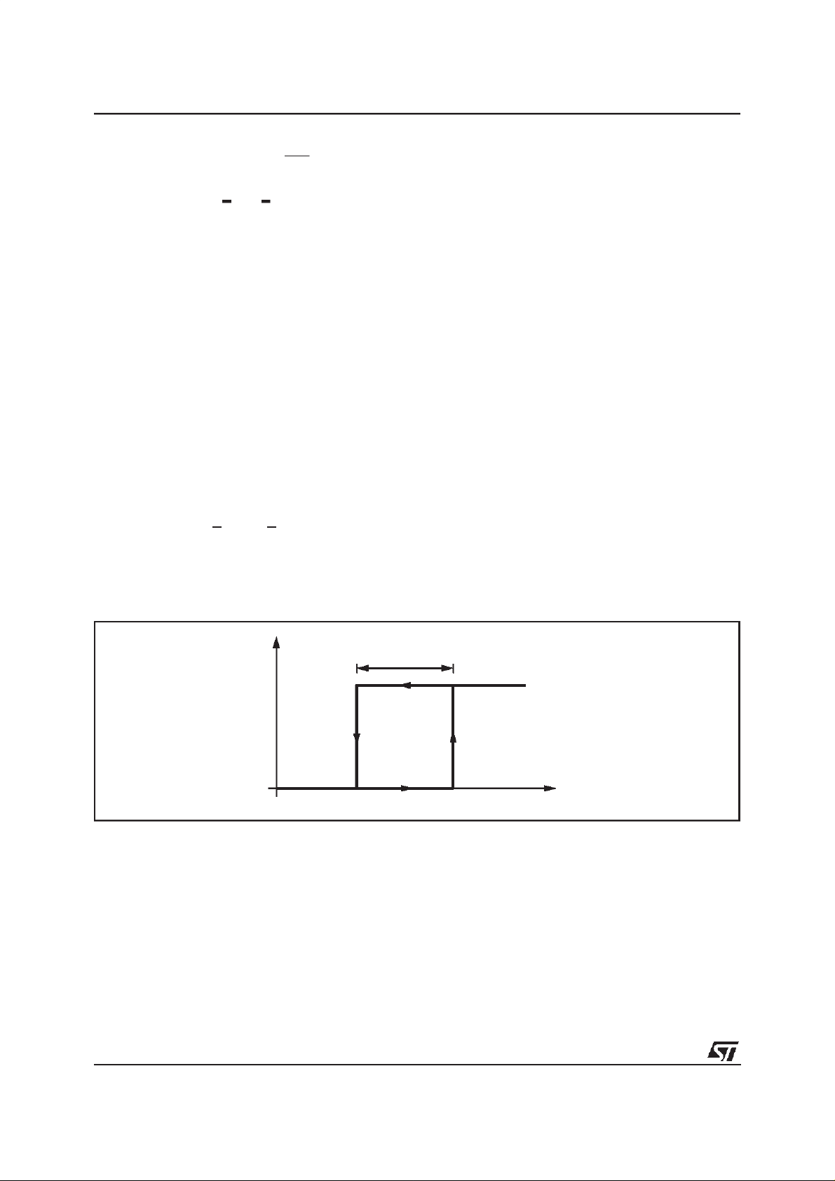
UNDERVOLTAGELOCK OUT
To avoid operation with non optimal drive of the
external power device, an Undervoltage Lockout
function is implemented. The OUT1 pin is forced
close to V
until the VCCsupply voltage has
SS
reached the Undervoltage Upper Threshold
(V
the lower hysteresis value (i.e. V
) value. If the supply voltage falls below
CCth2
CCth1 -VCChys)
the OUT1 will be again forced close to V
built-in hysteresis will thus avoid intermittent functioning of the device at low supply voltage that
may have a superimposedripple.
.
SS
. The
8/11
V
cchys
V
ccth
D94IN126B
V
s

L6353
DIM.
MIN. TYP. MAX. MIN. TYP. MAX.
a1 0.51 0.020
B 0.77 1.65 0.030 0.065
b 0.5 0.020
b1 0.25 0.010
D 20 0.787
E 8.5 0.335
e 2.54 0.100
e3 17.78 0.700
F 7.1 0.280
I 5.1 0.201
L 3.3 0.130
Z 1.27 0.050
mm inch
OUTLINE AND
MECHANICAL DATA
DIP16
9/11
L6353
DIM.
MIN. TYP. MAX. MIN. TYP. MAX.
A 1.75 0.069
a1 0.1 0.25 0.004 0.009
a2 1.6 0.063
b 0.35 0.46 0.014 0.018
b1 0.19 0.25 0.007 0.010
C 0.5 0.020
c1 45° (typ.)
D (1) 9.8 10 0.386 0.394
E 5.8 6.2 0.228 0.244
e 1.27 0.050
e3 8.89 0.350
F (1) 3.8 4 0.150 0.157
G 4.6 5.3 0.181 0.209
L 0.4 1.27 0.016 0.050
M 0.62 0.024
S
mm inch
8°(max.)
OUTLINE AND
MECHANICAL DATA
SO16 Narrow
(1) D and F do not includemold flashor protrusions.Mold flash or potrusions shall not exceed 0.15mm(.006inch).
10/11

L6353
Information furnished is believed to be accurate and reliable. However, STMicroelectronics assumes no responsibility for the consequences
of use of such information nor for any infringement of patents or other rights of third parties which may result from its use. No license is
granted by implication or otherwise under any patent or patent rights of STMicroelectronics. Specification mentioned in this publication are
subject to change without notice. This publication supersedes and replaces all information previously supplied. STMicroelectronics products
are not authorized for use as critical components in life support devices or systems without express written approval of STMicroelectronics.
The ST logo is a registered trademark of STMicroelectronics
2000 STMicroelectronics – Printed in Italy – All Rights Reserved
STMicroelectronics GROUP OF COMPANIES
Australia - Brazil - China - Finland - France - Germany - Hong Kong - India - Italy - Japan - Malaysia - Malta - Morocco -
Singapore - Spain - Sweden - Switzerland - United Kingdom - U.S.A.
http://www.st.com
11/11
 Loading...