


DESCRIPTION
The F-VHS Motor Driver COMBO IC includes a
double three phase brushless motor driver plus a
DC full bridge motor driverforVCRapplication.
The package is SDIP42 (38+2+2 pin ground
frame).
The device is realized in BCD technology with
power LDMOS outputstages.
The gate drive for high side stages is providedby
an internalcharge pump withtwo externalcapacitors. The first three phase motor driver is devoted
to the DRUMmotorcontrol.
The phase sequence update signal is provided initially by an external start-up signal (FSTART),
whose frequency is internally divided by four,
while, during normal operation, is provided by an
optical tacho convertersignal.
This signalis used as clockand reset for thestate
machine.
The regulation of the speed is externally provided
by means of PWM signal generated by the µP
(DPWM), without external sensing resistor. The
feedback to theµP unit is given by a suitable
open drain output signal (PUD) synchronized by
the internal state machine.
The second three phase motor driver is devoted
to the CAPSTAN control. While the DRUM will always spin in a fixed direction, the CAPSTAN motor needs a moresophisticatedlogic to control the
changes in spindirection.
The motor position detection is carried out by
means of three comparators for Hall effect sensors. The loop regulationfor this motor is still provided by theµP with the signals CPWM and
CDIR.
The LOADINGmotor section include a full bridge
DC motor driver. The motor operations are directly set by the inputsLPWM, LDIR according to
the truth table reportedon thepage5.
The device also includes a circuit for early thermal alarm, last thermal alarm and thermal shutdown with hysteresys.The output of this stage is
an opendrain,kept ON during normaloperations.
The THERM signal follows the inverted FSTART
signal between early warning and last warning
temperature, while remains in high impedance
(OFF) after lastwarning temperature and during
thermal shutdown.
L6287
POWER COMBO DRIVER
SDIP42
ORDERING NUMBER: L6287
The STANDBY state of thedevice is imposedby
THERMALSHUTDOWN
UNDERVOLTAGEON VCC SUPPLY
EXTERNALSIGNAL FSTART;
This state is imposed automatically after a defined time-out.
The time-out is realized by sensing the falling
edges of the FSTART signal: if no edges are recorded for a time interval greater than a certain
time constant, the STANDBY condition is generated.
The time constant is defined by the external capacitorCTO.
In the STANDBY state the main functions (upper
power stages, opto decoder, etc) of the device
are turned off in order to minimize the power consumption.
The device also implement a HEATER function.
The HEATER transistor is OFF during thermal
shutdown, undervoltagecondition and during normal workingmode.
The HEATER transistor is driven ON when the
externalSTANDBY condition is present according
to the followingtable:
FSTART HIGH LOW
HEATER OFF ON
During the ON condition,thespecified heater Ron
is not guaranteed if all the voltage supplies are
not at their minimumnominal value.
February 1997
This is advanced information on a new product now in development or undergoingevaluation. Details are subject to change without notice.
1/9
L6287
ABSOLUTE MAXIMUM RATINGS
Symbol Parameter Value Unit
V
DD
V
DC
V
DL
UPPER POWER
DS MAX
V
LOWERPOWER
V
DS MAX
V
CC
V
S
I
p1 Loading Motor Peak Current (T
pd Drum Motor Peak Current (T
I
pc Capstan Motor Peak Current (T
I
il Logic Input Low State Voltage -0.1 V
V
V
ih
V
therm
V
heat
(**) Not operative - STANDBYcondition
(***) Each motor driver
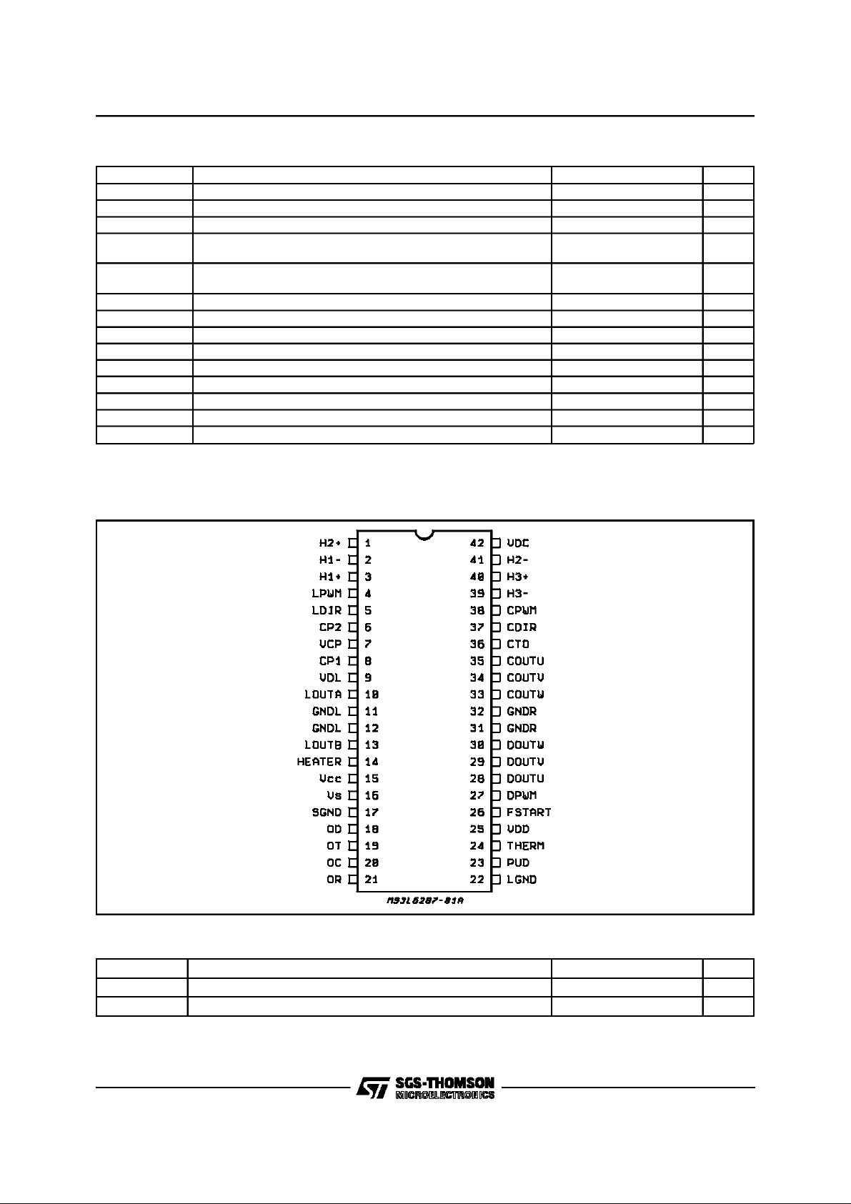
PINS CONNECTION
Drum Supply Voltage 20 V (**)
Capstan Supply Voltage 20 V (**)
Loading Supply Voltage 20 V (**)
Motor Output to Ground Voltage 20 V(***)
Motor Output to Supply Voltage 20 V (***)
Logic Supply Voltage 7 V
Special Supply Voltage 7 V
=1µs Duty Cycle = 2%) 1.6 A
on
=1µs Duty Cycle = 2%) 1.4 A
on
=1µs Duty Cycle = 2%) 1.8 A
on
Logic Input High StateVoltage 7 V
Open Drain Maximum Voltage 7 V
Open Drain Maximum Voltage 20 V (**)
THERMAL DATA
Symbol Parameter Value Unit
R
thj-amb
R
th j-pins
Note: Batwing pin.
2/9
Thermal Resistance Junction toAmbient 48 °C/W
Thermal Resistance Junction toPin 15 °C/W
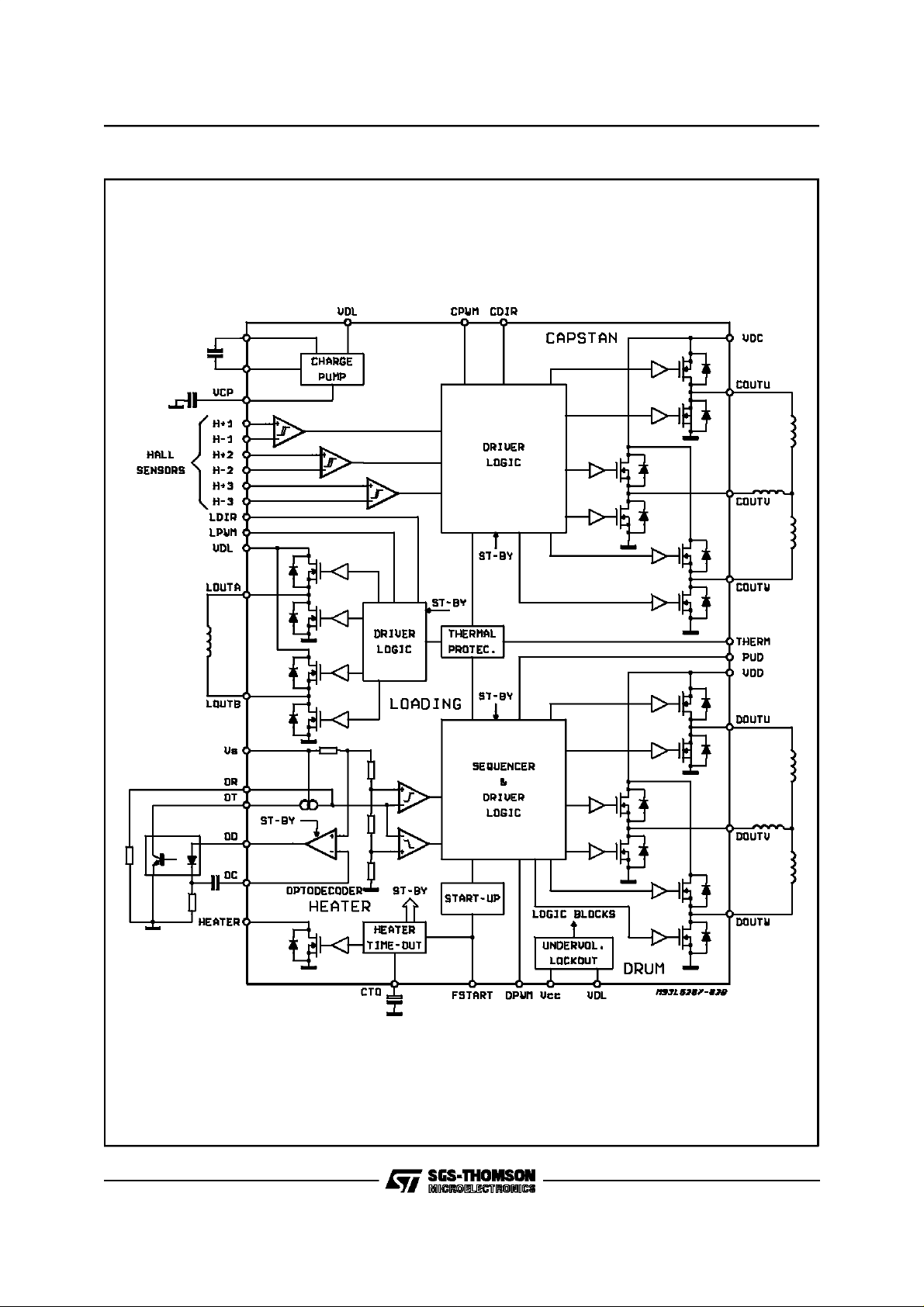
BLOCK DIAGRAM
CP1 = 0.01µF
CP2 = 0.1µF
L6287
3/9

L6287
PIN DESCRIPTION
VOLTAGE SUPPLIES (The power supply voltage VDD,VDC,VDL must be connected toghetherexternally)
V
DD
V
DC
V
DL
CC Logic voltage supply
V
GND Logic Ground
L
GND R Capstan + drum power ground
GND L Loading + Charge pump Power ground
S Analog voltage supply
V
GND Analog ground
S
Note: The V
DRUM MOTOR
D
OUTU
OUT V Winding Output V
D
OUTW Winding Output W
D
PWM PWM logic pulse input. Controlsignal generated by µP for dump motor current regulation.
D
UD Logic output position feedback generated by the translator logic
P
OD Optocoupler diode output
OC External capacitor fortacho-converter integrator
OT Input foroptocoupler transistor
OR Tacho-converter external resistor. This resistor defines the full-light currentlevel of the tacho.
CAPSTAN MOTOR
C
OUTU
OUT V Winding Output V
C
OUTW Winding Output W
C
PWM PWM logic pulse input. Controlsignal generated by µP for current regulation.
C
DIR Motor Direction Logic Input Signal
C
H1+
H1-
H2+
H2-
H3+
H3-
LOADING MOTOR
OUT A Winding Output A
L
OUT B Winding Output B
L
PWM PWM logic input.
L
DIR Directionlogic input
L
SERVICES
HEATER Open drain output forheater resistor
V
CP
CP1 Bootstrap Capacitor pin
CP2 Bootstrap Capacitor pin
THERM Open drain thermal alarm output
START Start-up logic signal for drum motor
F
CTO Time out capacitor output
Power supply voltage fordrump motor
Power supply voltage forcapstan motor
Power supply voltage forloading motor and charge pump
and VSPower Supply must betogether either at maximum or minimum value.
CC
Winding Output U
Winding Output U
Hall sensor differential input
Hall sensor differential input
Hall sensor differential input
Charge pump storage capacitor pin
4/9

L6287
ELECTRICALCHARACTERISTICS (Tj =0 to125°C; VCC=VS=5V±5%;VDC=VDL=VDD= 10 to 18V;
unless otherwisespecified.)
POWERSUPPLY
Symbol Parameter Test Condition Min. Typ. Max. Unit
(#)V
(#)V
(#)V
V
CC
V
S
V
CCth
# WARNING
The functionalityof the I.C. is guaranted in this voltage range. Nevertheless the specified operating voltages (V
according to the load characteristics.Proper cautions must be taken in the application in order to assure that the drain-source voltage across
each output power transistor does not exceed 20V max.
LOADING MOTOR
ACTIVATIONTRUTH TABLE
Drum Power Supply Voltage 10 18 V
DD
Capstan Power Supply Voltage 10 18 V
DC
Loading Power Supply Voltage 10 18 V
DL
Logic Power Supply Voltage 4.5 5.5 V
Sensor Power Supply Voltage 4.75 5.25 V
Undervoltage Threshold 3.6 4.4 V
DC,VDD,VDL), must be selected
INPUT OUTPUT
LPWM LDIR LOUTA LOUTB
0 0 LOW LOW
0 1 LOW LOW
1 0 HIGH LOW
1 1 LOW HIGH
Symbol Parameter Test Condition Min. Typ. Max. Unit
R
R
(*)I
(*)I
DSH
DSL
OL
High Side R
DSonH
Low Side RDSonL 2 Ω
DC Output Current 800 mA
Peak Output Current DUTY CYCLE = 10%;
pl
t
ON
=500ms
2 Ω
1A
DRUM MOTOR
Symbol Parameter Test Condition Min. Typ. Max. Unit
DC Output Current 400 mA
Peak Output Current 600 mA
Peak Output Current DUTY CYCLE = 10%;
t
= 500ms
ON
800 mA
High Side RDSonH 1.6 Ω
Low Side RDSonL 1.6 Ω
(*)I
(*)I
R
R
I
cd
cdp
pdb
DSH
DSL
CAPSTANMOTOR
Symbol Parameter Test Condition Min. Typ. Max. Unit
I
co
(*)I
cop
(*)I
pob
R
DSH
R
DSL
(*) WARNING
These current values are compatible with the structure of the IC power structure. Nevertheless the use of these current levels could produce
junction temperatures thatforce IC outsideof the operative range due to the thermalcharacteristics of the choosen package.
DC Output Current 800 mA
Peak Output Current 1 A
Peak Output Current DUTY CYCLE = 10%;
t
= 1ms
ON
1.5 A
High Side RDSonH 1 Ω
Low Side RDSonL 1 Ω
5/9

L6287
ELECTRICALCHARACTERISTICS (continued)
DRUM TACHO CONVERTER
Symbol Parameter Test Condition Min. Typ. Max. Unit
I
od
I
ot
I
oc
vs I
I
ot
V
ref
V
OC
V
thr1
V
thr2
t
pud
I
pud1
Note 1: The suggested C
Open Loop OutputCurrent Vod= 1V; Ioc= 100µA (Note 1) 30 60 mA
Full Light Current Range 0.5 3 mA
Sink Current Vor=0;Iod= 0 0.2 0.5 µA
Mismatch 5 10 %
or
Opto Resistor Reference
Voltage
Open Loop OptoCapacitor
Voltage
VS = 4.75V 3.36 3.72 V
S = 5V 3.54 3.91 V
V
= 5.25V 3.72 4.11 V
V
S
VOD= 1V see Fig.1
V
V
V
S
S
S
= 4.75V
=5V
= 5.25V
2.75 V
Clock Threshold Voltage VS= 4.75V 2.19 2.42 V
= 5V 2.30 2.54 V
V
S
= 5.25V 2.42 2.67 V
V
S
Reset Threshold Voltage VS= 4.75V 0.30 0.33 V
= 5V 0.32 0.35 V
V
S
S = 5.25V 0.33 0.37 V
V
µP Syncro Pulse Duration 1 3 µs
Open Drain Sink Current VO = 0.4V 5 mA
external capacitor value is 5µF(±5%)
opt
HALL COMPARATOR
Symbol Parameter Test Condition Min. Typ. Max. Unit
V
in
I
b
V
of
V
hy
Input Voltage Range 0.5 2.7 V
Input Bias Current 1
µ
Input Offset Voltage 8 mV
Switchable Hysteresys Vref = 1.5V; 10 40 mV
A
THERMAL PROTECTION
Symbol Parameter Test Condition Min. Typ. Max. Unit
I
therm
T
s
T
sdh
T
al1
T
al2
NOTE 1: Therm output stage is on in the normal temperature range
NOTE 2: In the Tal-Tll temperature range therm signal follows the inverted Fstart signal. After Tll temperaturethisoutput is always in high
Open Drain Sink Current V
Shutdown Temperature 155 170 185
Shutdown Hysteresis 60
Early Warning Temperature Ts -40
Last Warning Temperature (see note 2) Ts -20 °C
impedance.If thermal shutdown is reached this pin will remain in this state until the shutdown hysteresys will be recovered.
= 0.4V (seenote 1) 5 mA
out
o
C
o
C
o
C
HEATER
Symbol Parameter Test Condition Min. Typ. Max. Unit
R
V
dsheat
heat
Heater R
DSon
Heater Voltage 18 V
3 ohm
6/9

ELECTRICALCHARACTERISTICS (continued.)
L6287
LOGIC LEVELS FOR DIGITALINPUTS(C
A pull up resistor R
i
is connected between the C
PWM,CDIR,DPWM,FSTART,LPWM,LDIR
DIR,FSTART,LPWM,LDIR
inputs pads; C
)
and D
PWM
are left unconnected.
Symbol Parameter Test Condition Min. Typ. Max. Unit
V
il
ih Input High Voltage 2 V
V
i Pull Up Resistor 3.5 10.5 Kohm
R
Input Low Voltage 0.8 V
TIME OUT STAGE
Symbol Parameter Test Condition Min. Typ. Max. Unit
I
cto
Note 1: The suggestedexternal capacitor value is Cto=1µF(±20% max) for f
Time Out Output Current (Note 1) 5 20 uA
= 20KHz.
START
Figure 1: OptocircuitOpenLoop OC Voltage.
PWM
7/9

L6287
SDIP42PACKAGE MECHANICAL DATA
DIM.
mm inch
MIN. TYP. MAX. MIN. TYP. MAX.
A 5.08 0.20
A1 0.51 0.020
A2 3.05 3.81 4.57 0.120 0.150 0.180
B 0.38 0.46 0.56 0.0149 0.0181 0.0220
B1 0.89 1.02 1.14 0.035 0.040 0.045
c 0.23 0.25 0.38 0.0090 0.0098 0.0150
D 36.58 36.83 37.08 1.440 1.450 1.460
E 15.24 16.00 0.60 0.629
E1 12.70 13.72 14.48 0.50 0.540 0.570
e 1.778 0.070
e1 15.24 0.60
e2 18.54 0.730
e3 1.52 0.060
L 2.54 3.30 3.56 0.10 0.130 0.140
E
E1
A2
A1
LA
BeB1
D
42
1
22
21
c
SDIP42
e1
e2
E
.015
0,38
Gage Plane
e3
e2
8/9

L6287
Information furnished is believed to be accurate and reliable. However, SGS-THOMSON Microelectronics assumes no responsibility for the
consequences of use of such information nor for any infringement of patents or other rights of third parties which may result from its use. No
license is granted by implication or otherwise under any patent or patent rights of SGS-THOMSON Microelectronics. Specification mentioned
in this publication are subject to change without notice. This publication supersedes and replaces all information previously supplied.
SGS-THOMSON Microelectronics products are notauthorized foruse as criticalcomponentsin lifesupport devicesor systemswithout express
written approval of SGS-THOMSON Microelectronics.
1997SGS-THOMSON Microelectronics – Printedin Italy – All Rights Reserved
SGS-THOMSON Microelectronics GROUP OF COMPANIES
Australia - Brazil - Canada - China - France - Germany - HongKong -Italy- Japan - Korea - Malaysia - Malta - Morocco - The Netherlands -
Singapore - Spain - Sweden - Switzerland - Taiwan - Thailand - United Kingdom - U.S.A.
9/9
 Loading...