

L6285
3 CHANNELS MULTIPOWERSYSTEM
ADVANCE DATA
CHANNEL-A AND CHANNEL-B FOR UNIPOLAR STEPPER MOTORS
– LOWSIDE: R
– HIGH SIDE ; R
DSON
DSON
= 1.2Ω
= 1.2Ω
CHANNEL-CFOR DC MOTORS
– LOWSIDE: R
– HIGH SIDE: R
DSON
DSON
= 1.7Ω
= 1.2Ω
CHOPPING MODE DRIVING FOR C.L. CURRENT CONTROL ON CHA AND CHB AND
O.L. VOLTAGECONTROL ONCHC.
INTERNALFOUR DRIVINGLATCHES
16 BIT INTERNAL SHIFTREGISTER
DIRECTINTERFACE TO µP
SERIALDRIVINGSEQUENCE LOADING
CMOSCOMPATIBLEINPUTS
PRE-ALARMOUTPUT SIGNAL
THERMAL SHUTDOWN
DESCRIPTION
This Combo Motor Driver uses large scale integration to incorporate several functions into the
same chip.
1) Two unipolar steppermotor driver
2) A full bridgeDC motor driver
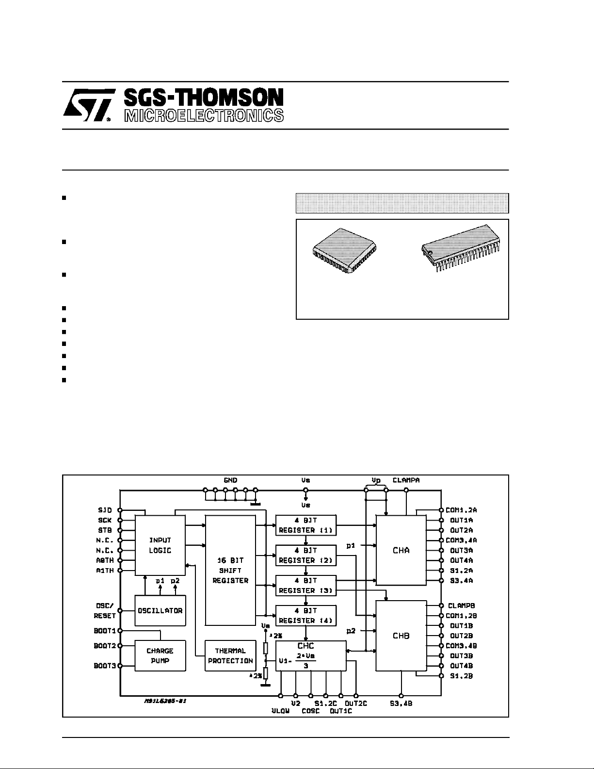
BLOCK DIAGRAM
MULTIPOWER BCD TECHNOLOGY
PLCC44 SDIP42
ORDERING NUMBERS:
L6285 L6285S
3) Serial microprocesor interface
The poweroutput stages areDMOS and the input
can be interfaced to a CMOS Microprocessor
logic.
The phase current in the unipolar stepper motor
windings is controlled by two external sensing resistors in fixed frequency choppingmode.The oscillator block provides clocks each other 180° out
of phase to the two stepper motor driver in order
to avoidsymultaneous currentpeaks.
For the DC motor driver is used a bridge; the
RMS voltage to supply this motor is fixed by a
May 1994
This is advanced informationon a new product now in development or undergoing evaluation. Details are subject tochange without notice.
1/16
L6285
simple PWMopen loop. The 3 motorsare controlled by the micro through 4 latches of 4 bit each.
The loading of these registers is in serial mode.
The I.C. operates at 5V supply forthe logic and at
PINCONNECTION (Top view)
PWGND
OUT1A
S1,2A
OUT2A
CLAMPA
OUT3A
S3,4A
OUT4A
BOOT1
BOOT3
GND
7
8
9
10
11
12
13
14
15
16
17
COM3,4A
PWGND
SID
BOOT2
P
COM1,2A
V
PLCC44
STB
SCK
S1,2C
OUT2C
123564
2322211918 20 28272624 25
S
V
N.C.
OUT1C
COM1,2B
N.C.
A0TH
P
V
A1TH
PWGND
COM3,4B
40414244 43
39
38
37
36
35
34
33
32
31
30
29
V2
OSC RESET
PWGND
OUT1B
S1,2B
OUT2B
CLAMPB
OUT3B
S3,4B
OUT4B
VLOW
COSC
GND
D94IN067
24V supply for the power stages. The packages
are SDIP42 and PLCC44 with 6 pins devoted to
ground and to sink out the heat produced by
powerdissipation.
OUT2C
COM1,2A
COM3,4A
PWGND
OUT1A
S1,2A
OUT2A
CLAMPA
OUT3A
S3,4A
OUT4A
BOOT1
BOOT3
BOOT2
1
2
V
3
P
4
N.C. COM3,4B
5
6
7
8
9
10
SDIP42
11
12
13
14
15
16
GND
17
N.C.
18
19
SID
20
SCK
21
STB
D94IN060A
42
41
40
39
38
36
35
34
33
32
31
30
29
28
27
26
25
24
23
22
S1,2C
OUT1C
COM1,2B
V
P
PWGND37
OUT1B
S1,2B
OUT2B
CLAMPB
OUT3B
S3,4B
OUT4B
V
LOW
C
OSC
GND
V2
OSC RESET
A1TH
A0TH
V
S
ABSOLUTE MAXIMUM RATINGS
Symbol Parameter Value Unit
V
V
V
I
LOW
I
HIGH
I
pLOW
I
pHIGH
V
bout
Power Supply Voltage 30 V
P
Logic SupplyVoltage 7 V
S
Logic Input Voltage -0.3 toVS+ 0.3 V
in
Low Side DMOS max DC Current 1 A
High Side DMOS max DC Current 1 A
Low Side DMOS max Peak Current (1µs On; 50µs OFF) 2 A
High Side DMOS max Peak Current(1µs On; 50µsOFF) 2 A
Max Output Voltage of Stepper Motor Driver(transient
60 V
rcirculation)
V
1;2 Max Voltage ON Vsense (CHA/CHB) -1 to2 V
sense
3 Max Voltage ON V
V
sense
Ι
fdDC
Ι
fdpk
Max DC Currentof Forward Diode(DMOS Source DrainDiode) 1 A
Max Peak Current of ForwardDiode (DMOS Source Drain
(CHC) -1 to 2 V
sense
2A
Diode) (1µs On;50µs OFF)
P
tot
T
op
T
stg
Total Power Dissipation (Tpins = 90°C)
With minimized dissipatingcopper area (T
amb
=70°C)
5
1.6
Operating Temperature Range 0 to 150 °C
Storage Temperature Range -40 to 150 °C
THERMAL DATA (PLCC44)
Symbol Description SDIP42 PLCC44 Unit
R
th j-pins
R
th j-amb
Thermal Resistance Junction-pins
Thermal Resistance Junction-ambient
Max.
Max.
15
48
12
50
W
W
°C/W
°C/W
2/16
PINDESCRIPTION
SDIP42
o
N
42 1 S1,2C Full bridge common source output to separate between power GND
1,41 2,44 OUT 1C, OUT 2C Output of the channel C bridge.
2 3 COM 1,2A High side DMOS channel A for current chopping in the windings
3,39 4,42 V
4 5 COM 3,4A High side DMOS channel A for current chopping in the windings
6,37 6,7,39,40 GND PowerGround and heatsinkpins.
7,9,
11,14
8 9 S1,2A ChannelA sourcesof theDMOS OUT 1A, OUT 2A. A sensing resistor
10,33 11,35 CLAMP A, CLAMP B These pinshave to be connected to an external zener diodeto
12 13 S3,4A Channel Asources of the DMOSOUT 3A,OUT 4A. A sensingresistor
14 15 BOOT 1 A capacitor between this pin and V
15 16 BOOT 3 A capacitor between this pinand internal diodes allows the change
16,27 17,29 GND Logic Ground and Heatsink pins.
18 18 BOOT 2 Charge pump oscillator output.
19 19 SID Serial data input.
20 20 SCK Serial clock for serial data input.
21 21 STB Strobe to transfer the16 bit shift register contentsto the latch
5,17 22,24 NC Notconnected.
22,39 23 V
23,24 25,26 A0TH / A1TH Open collector outputs for thermal informations to the µP.
25 27 OSC/ RESET An RC network connected to this pin defines the oscillatorfrequency
26 28 V2 A voltage to this pindefines the outputduty cycle ofChannel C.
28 30 C
29 31 V
30,32,
34,36
31 33 S 3, 4B Same as S 3, 4A,but for channelB.
35 37 S 1, 2B Same as S 1, 2A,but for channelB.
38 41 COM 3, 4B Same as COM 3, 4A, but for channel B.
40 43 COM 1, 2B Same as COM 1, 2A, but for channel B.
PLCC44
o
N
8,10
12,14
32,34
36,38
Name Functions
and logic GND.
connected pins to OUT 1A, OUT 2A.
p
Power Supply Voltage.
connected topins OUT 3A, OUT 4A.
OUT 1A, OUT 2A
Low side DMOS outputs of channel A stepper motor driver.
OUT 3A, OUT 4A
has to be connected from this pin and ground, forcurrent controlof
phase1,2 A.
clamp the output voltage spikes of channel A/B.
has to be connected from this pin and ground, forcurrent controlof
phase3,4 A.
high side DMOS driver gate.
pump to transfer energy to the capacitor at the pin BOOT 1.
registers.
s
Logic Supply Voltage.
for stepper drivers. When OSC/RES is <1V, a reset signal is
internally generated.
osc
A capacitor connected to thispin defines the chopping frequency of
channel C.
low
This pin is low when thechopping low voltage (V2 low level) is
selected; it is in highimpedance when the chopping high voltage(V2
high level) is selected. Only for CHC operation.
OUT4B, OUT3B
Low side DMOS outputs of channel B stepper motor driver.
OUT2B ,OUT1B
stores theovervoltage for each
p
L6285
3/16
L6285
ELECTRICAL CHARACTERISTICS (Tj=25°C, Vs=5V, Vp= 24V unless othewise specified)
Symbol Parameter Test Conditions Min. Typ. Max. Unit
V
p
I
p
V
s
I
s
LOGICLEVEL
Symbol Parameter Test Conditions Min. Typ. Max. Unit
V
inL
V
inH
I
inL
I
inH
CHANNEL A AND CHANNEL B (UNIPOLARMOTORS)
Symbol Parameter Test Conditions Min. Typ. Max. Unit
R
DSONL
R
DSONH
Power Supply Voltage 9 26.5 V
Quiescent Power Supply
(note 1) 7 mA
Current
Logic SupplyVoltage 4.5 5.5 V
Quiescent Logic Supply
(note 1) 20 mA
Current
Input Low Voltage -0.3 1.35 V
Input High Voltage 3.15 VS+0.3 V
Input Low Current Vin =V
Input High Current Vin =V
inL
inH
-10 µA
10 µA
Low Side DMOS ON Res. IDS = 0.7A 1.2 Ω
High Side DMOS ON Res. IDS = 0.7A 1.2 Ω
I
DSSL
Low Side DMOS Leakage
VDS= 60V;output OFF 2 mA
Current
I
DSSH
High Side DMOS Leakage
VP = 30V; VO= 0V -1.5 mA
Current
V
REF
Voltage reference to the
Comparator
LEVEL 1
LEVEL 2
LEVEL 3
LEVEL 4
T
d
Turn OFF Delay on HIGH
Side DMOS afterthe
(note 2)
100
220
340
465
125
250
375
500
150
280
410
535
1 µs
Sensing Current Reach the
Threshold Value
f
max
Max Chopping Frequency 40 KHz
CHANNEL C (DC MOTORS)(see Fig.5)
Symbol Parameter Test Conditions Min. Typ. Max. Unit
f
osc
DC Duty Cycle V2 = 1/2V
I
b2
V
low
R
DSONH
R
DSONL
I
LH
I
LL
V
fddc
f
max
V
boot
I
Lboot
Oscillator Frequency Cosc = 3.3nF; V1 = 2/3VS 17 22 28 KHz
S
72 75 81 %
Comparator Input Bias V2 = 200mV -1 µA
Open Drain Output I = 5mA 0.2 0.4 V
High Side DMOS ON Res. IDS= 0.7A 1.2 Ω
Low Side DMOS ON Res. IDS= 0.7A 1.7 Ω
HSD MOS Leakage Current VP= 30V; VO=0V -1 mA
LSD MOSLeakage Current VO = 30V; Vsense = 0V -1.5 mA
Forward Diode DC Voltage
I
= 0.7A 1.4 2 V
fdcc
(DMOS Diode)
Max Chopping Frequency 40 KHz
Voltage on pin Boot1 Vp+7 V
Leakage Currenton pin Boot1 V
bott=Vp
+12V; Vp= 26.5V 200 µA
mV
mV
mV
mV
4/16
ELECTRICAL CHARACTERISTICS (continued)
OSCILLATOR (see Fig.6)
Symbol Parameter Test Conditions Min. Typ. Max. Unit
f
osc
Oscillator Frequency
COSC = 3.3nF; R
= 10KΩ 27 41 46 KHz
OSC
Pin OSC/RESET
V
T
dsc
reset
Capacitor Discharge Time
(protect deadtime)
C
= 3.3nF; R
OSC
(see Fig.1)
OSC
= 10KΩ
0.8 1.4 2 s
Reset Threshold Voltage 1 V
INTERFACE TIMING
Symbol Parameter Test Conditions Min. Typ. Max. Unit
t1 SCK Data Clock Cycle (see Fig. 2) 200 ns
t2 SCK Data Set-upTime 30 ns
t3 SCK Data Hold Time 20 ns
t4 SCK-STB Interval Time 30 ns
t5 STB Pulse Width 100 ns
Note 1: No output loaded; all register tolow condition;no resetapplied; VP= 26.5V;VS= 5.5V
Note 2: The effectof theinternal filter (RC Network)is not considered.
L6285
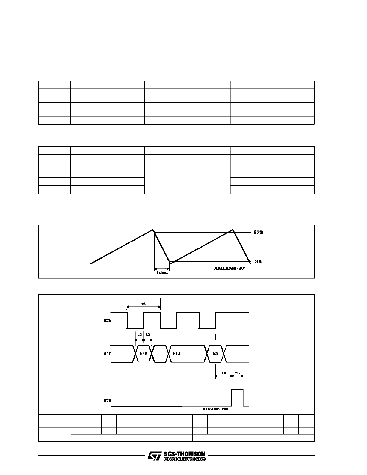
µ
Figure 1: Discharge timet
or ProtectionTime
dsc
Figure 2: InterfaceTiming (Serialloading Mode)
Serial
Input Data
b15
b14 b13 b12 b11 b10 b9 b8 b7 b6 b5 b4 b3 b2 b1 b0
D15
D3 D2 D1 D0 D3 D2 D1 D0 D3 D2 D1 D0 D3 D2 D1 D0
Register 4 Register 3 Register 2 Register 1
D0
5/16

L6285
BLOCK DIAGRAM DESCRIPTION
(see Block Diagram)
Inside the I.C. there are two unipolarstepper mo-
tor drivers,one bridge driver for DC motor, 4x4 bit
latch registers, one shift register. the input logic,
the charge pump, and the thermal protection.
The following conditions are valid for all the 3
driver sections:
1)When the osc/respin is tied to GND, an internal reset signal is generated which switches
off all the outputs and resets the internal registers.
2)The conditions1 is valid also duringpower on
and power off transitions.
3)During power on and power off, the I.C. is
safe for any conditionsof V
and V
S
p
3)If Vpis present and VSdesappears, the outputs are switchedoff.
InputLogic
The input CMOS logic interfacesthe microprocessor logic to the 4 registers. An integrated Schmitttrigger circuit is used to improve noise immunity
ateach logic input.
The datais introducedin the 16bitshift register by
the SID pin. The first bit b 15 after 16 clock applied to SCK pin will be the D15 of the shift register.
On the falling edge of STB the 16 bits of the shift
register are transferred to the outputs of the 4
latchregisters. Fig 2shows the timing.
CHA and CHB Stepper Motor Drivers
Registers
The ComboMotor Driver controlsthe 3 channels using 4 latch registersof 4 bit each:
CHANNEL A
CHANNEL A
CHANNEL A
CHANNEL A
CHANNEL B
CHANNEL B
CHANNEL B
CHANNEL B
LEAST
MOST
LEAST
MOST
CHANNEL C
CHANNEL C
CHANNEL C
CHANNEL C
REGISTER 1
REGISTER 2
REGISTER 3
REGISTER 4
D0
D1
D2
D3
D0
D1
D2
D3
D0
D1
D2
D3
D0
D1
D2
D3
=
=
=
=
=
=
=
=
=
=
=
=
=
=
=
=
PHASE 1A
NPHASE 2A
PHASE 3A
NPHASE 4A
PHASE 1B
NPHASE2B
PHASE 3B
NPHASE4B
D/A CHANNEL A
D/A CHANNEL A
D/A CHANNEL B
D/A CHANNEL B
INPUT 1
INPUT 2
V2 VOLTAGE
V2 VOLTAGE
Register 1/2 Output Status (CHA and CHB). See note 1
D0 D1 D2 D3 OUT1 A/B OUT2 A/B OUT3 A/B OUT4 A/B
0
1
1
0
0
0
0
0
1
0
0
0
0
1
1
1
0
0
ALL THE OTHERS OFF OFF OFF OFF
0
0
1
1
1
0
0
0
0
0
0
0
0
0
0
1
1
1
OFF
ON
ON
OFF
OFF
OFF
OFF
OFF
ON
OFF
OFF
OFF
OFF
ON
ON
ON
OFF
OFF
OFF
OFF
ON
ON
ON
OFF
OFF
OFF
OFF
Register 3 Current Reference (D/AOUTPUT)
DO D1 REFER. VOLTAGE CHANNEL A
0.125 V
0.250 V
0.375 V
0.500 V
6/16
0
0
1
1
0
1
0
1
D2 D3 REFER. VOLTAGE CHANNEL B
0
0
1
1
0
1
0
1
0.125 V
0.250 V
0.375 V
0.500 V
OFF
OFF
OFF
OFF
OFF
OFF
ON
ON
ON

REGISTER4 (CHC).See note 2
D0 D1 D2 D3 OUT1 C OUT2 C
OFF
X
0
1
0
1
1
0
1
0
0
1
0
1
X
0
0
1
1
0
1
0
1
0
1
0
1
0
1
1
1
1
1
1
0
0
1
1
0
0
0
OFF
1
V
1
1
1
0
0
1
1
0
0
1
1
P
GND
GND
V
P
CHOPPING; V2 LOW LEVEL
V
P
CHOPPING; V2 HIGH LEVEL
OFF
V
P
OFF
V
P
OFF
OFF
GND
V
P
GND
CHOPPING; V2 LOW LEVEL
V
P
CHOPPING; V2 HIGH LEVEL
V
P
OFF
V
P
OFF
V
P
L6285
Note 1: Low side DMOS status (DM1/2 inFig. 4)
Note 2: Bridge status(see Fig. 3): OFF = tristate;V
P
Figure 3: CHC Chopping Characteristics
=,DM3/4ON; GND =DM1/2 ON
7/16

L6285
These two channels drive two unipolar stepper
motorsin choppingmode. The basic channel configuration is shown in Fig 4. by considering well
known the PWM Current Control Loop behaviour
here below only particular trick are underlined.
During DM3 off period the low side DMOS DM1
and DM2 are switched on to reduce the power
dissipation.
Figure.4: Unipolarmotor driver CHA(or CHB)
The drain overvoltagesgenerated because of the
stray inductance of the motor windings are limited
by connecting the DZ1 externalzener diode to the
clamp pin.. The diodes CL1 and CL2 are integrated as far as the CL3 diode which limits the
negative voltage at pin COM1.2. An internal RC
network (1µs) is realized to filter the sensing resistor signal.
8/16

L6285
CHC DC MotorDriver
The DC motor driver is a DMOS full bridge with a
PWM Open Loop Voltage Control. Fig.5 shows
the theory of operation. The C
Capacitor is
osc
charged by a constant current source. The oscillating voltage value is from 0V to the V1 level internally fixed at V1 = 2/3 V
. The output duty cy-
S
Figure.5:DC MotorDriver CHC
cle is controlled by the V2 voltage. The operational range of V2 is from 200mV to V1. Fig.3
shows the DMOS status during PWM: t
t
bridge configurations. While the PWM Duty
OFF
ON
and
Cycle defines the motor speed (not controlled
since the loop is open),the logic level of IN1 and
IN2 can choose the directionof the motor.
9/16

L6285
OscillatorFor Clock and Reset Generation
The oscillatorblock provides for two functions:
1)Generate an internal reset signal when the
voltage at pin osc/res is below 1V. The reset
signal switches off all the outputs and resets
the logic registers.
2)Generate,when the pin osc/resis left freetwo
syncro signals p1 and p2 for the clock of the
PWM Current Control of the two stepper
driverblocks
The oscillator operates like the 555 concept in
Figure 6: Oscillator Concept
which the capacitor voltage oscillates between
1/3V
2/3VS(Fig.6). The oscillator frequencyis 2
S
times the choppingfrequency in orderto generate
the two syncro signals at operative 20KHz PWM.
The t
V
TH1
The discharge time T
= charge timeof Cosc is defined by R
CH
and V
( thresholdvoltages)and C
TH2
is practically only defined
dsc
osc
osc
.
by Cosc and the internal discarge resistor Rdsc.
The t
is also the time lockout during which the
dsc
RS FF cannot read the Comparator output (see
Fig. 4)
,
10/16

L6285
Charge Pump
The charge pump circuitry generates the overvoltage needed to drive the gate of the high side output DMOS power transistors.It is realized by using two external capacitors (C1 and C2) and two
integrateddiodes thatoperate as a fullwave recti-
Figure 7: Charge Pump Circuit
fier (see Fig. 7). The oscillator peak to peak output voltage is stored by C2 and summed to the
Power Supply Voltage V
..
p
The voltagepresent at the pin BOOT1,is then the
overvoltageneeded to supply the gate of the high
side DMOS drivers.
THERMAL PROTECTION
The thermal protection shuts down the chip be-
A0TH A1TH THERMAL PROTECTION CIRCUIT STATUS
0
1
1
0
0
0
1
1
OK
PREALARM
ALARM
NOT POSSIBLE
APPLICATION INFORMATION
A typical application circuit is shown in Fig.8. By
this application it is possible to drive twounipolar
stepper motors (M1,M2) and one DC motor(M3).
As it can be seen, only two external Zener diodes
(D1,D2) are needed to clamp the voltage transients generated by the stray inductance of the
motor windings. This is recommended when the
peak current is not more than three to four hundred mAmps. For a power supply voltage of
=24V ±10%, D1=D2 must be 30V ±5%-1W
V
P
(1N4751A or equivalent).Both the V
and the V
P
pins need bypass capacitors (C1,C2,C3); to supply the high-side DMOS (Source Transistors) at
pin.15 ,only two externalcapacitors (C4,C5) complete the charge pump circuitry. The oscillator frequency, that is twice the chopping frequency for
M1 and M2, is mainly defined by the network
R6C6:
=[0.69 (Rch+Rdsc)C
f
osc
R
=R6 ; R
ch
dsc
=600 ohm typ.
]-1, where
osc
fore itcan reach adangerous temperature.
Additional informations to the microprocessor are
availableat the A0TH, A1THpins.
OPERATING
OPERATING
THERMAL SHUTDOWN
At the same time, the lockoutduration (or protection window) needed for a correct chopping behavior,is given by :
lockout
= 0.69 R
dscCosc
T
The shown values (fig.8) give a nominal fre-
quency a little bit more than 41KHz and a protectionwindow of 1.4 µs roughly.The Schottkydiode
D3 and thepull-up resistor R5 driven viaan opencollector transistor can generate the Reset function. The chopping current is sensed across R1
A/B; R2 A/B that must be of a not inductive type.
S
The DC motor PWM Open Loop Voltage Control
operates at a frequency defined by C7, charged
with a typical constant current source (I = 240
µA), up to V1 = 0.67 V
S
time is very short,it can be written:
f
osc
=I/C
V1, where C
osc
Tha values indicated in figure give a typical frequencyof about 22 KHz.
. Since the discharge
= C7.
osc
11/16

L6285
Figure 8: Typical Application Circuit
The duty cycle DC can be chosen between two
possibilities (High and Low ) than can be defined
externally by the resistors R7, R8 and R9: Fig.5
let well understand how to calculate the dividers
that fix V2 H (wider t
) and V2 L (wider t
on
off
). It
may be needed to drive stepper motors that require a higher peak current than told above. In
this case each motor phase requires a particular
application arrangement(see Fig.9b).In Fig.9aall
Figure 9a: Output Configuration as it is obtained
by the ApplicationCircuit
the protection components are integratedwith the
exception of Z1. In Fig.9b the clamp of the voltage spikes generated by the stray inductance Ls
is achieved using Transil protection T1 and T2
that works also as additional diodes during current recirculation at the phase change. The diode
D1, externally connected, is recommended at the
highest working current levels and/or when the
supplied voltage (plus Back EMF) at the end of
the motor windingis too much unbalanced.
Figure9b: OutputConfiguration at HigherOper-
ating Currents
12/16

L6285
THERMAL CHARACTERISTICS
The cooling of the device is obtained by soldering
its ground pins on a proper p.c.b copper side ,
acting as a true heatsink. By considering four
squared side as in Fig.10, the junction to ambient
Figure 10: Four ”on board” Square Heatsink
thermal resistance has been measured (see
Fig.11). The typical transient thermal resistance
versus values of single pulse width of power is
shown in Fig.12. In general these thermal characteristics are very important to the designer to optimizethe L6285 applications.
Figure 11: Typical R
vs.lenght ”l” (Fig. 10)
th j-amb
Figure12: TypicalTransient Thermal Resistance
vs.Time or PulseWidth
13/16

L6285
SDIP42PACKAGE MECHANICALDATA
DIM.
mm inch
MIN. TYP. MAX. MIN. TYP. MAX.
A 5.08 0.20
A1 0.51 0.020
A2 3.05 3.81 4.57 0.120 0.150 0.180
B 0.36 0.46 0.56 0.0142 0.0181 0.0220
B1 0.76 1.02 1.14 0.030 0.040 0.045
c 0.23 0.25 0.38 0.0090 0.0098 0.0150
D 37.85 38.10 38.35 1.490 1.50 1.510
E 15.24 16.00 0.60 0.629
E1 12.70 13.72 14.48 0.50 0.540 0.570
e 1.778 0.070
e1 15.24 ‘0.60
e2 18.54 0.730
e3 1.52 0.060
L 2.54 3.30 3.56 0.10 0.130 0.140
E
E1
A2
A1
LA
BeB1
D
42
1
22
F
21
c
SDIP42
e1
e2
E
.015
0,38
Gage Plane
e3
e2
14/16

PLCC44 PACKAGE MECHANICAL DATA
L6285
DIM.
MIN. TYP. MAX. MIN. TYP. MAX.
A 17.4 17.65 0.685 0.695
B 16.51 16.65 0.650 0.656
C 3.65 3.7 0.144 0.146
D 4.2 4.57 0.165 0.180
d1 2.59 2.74 0.102 0.108
d2 0.68 0.027
E 14.99 16 0.590 0.630
e 1.27 0.050
e3 12.7 0.500
F 0.46 0.018
F1 0.71 0.028
G 0.101 0.004
M 1.16 0.046
M1 1.14 0.045
mm inch
15/16

L6285
Information furnished is believed to be accurateand reliable. However, SGS-THOMSON Microelectronicsassumes no responsibility for the
consequences of use of such informationnor for any infringement of patents or other rights of third parties which may result from its use. No
license is granted by implication or otherwise under any patent or patent rights of SGS-THOMSON Microelectronics. Specifications mentioned in this publication are subject to change without notice. This publication supersedes and replaces all information previously supplied.
SGS-THOMSON Microelectronics products are not authorized for use as critical components in life support devices or systems without express written approval of SGS-THOMSON Microelectronics.
1994 SGS-THOMSON Microelectronics - All RightsReserved
SGS-THOMSON Microelectronics GROUP OFCOMPANIES
Australia- Brazil- France - Germany -Hong Kong - Italy - Japan- Korea -Malaysia - Malta - Morocco - The Netherlands- Singapore - Spain
- Sweden- Switzerland - Taiwan - Thaliand - United Kingdom - U.S.A.
16/16
 Loading...