

L6280
THREE CHANNELS MULTIPOWER DRIVER SYSTEM
ADVANCE DATA
PROGRAMMABLE CONFIGURATION
(CHANNELS1 AND2)
OUTPUT CURRENT UP TO 1A (CHANNELS
1AND2)
1 SENSEPER CHANNEL
OUTPUTCURRENT CHANNEL 3 UP TO 3A
DIRECT INT ERFACE TO MICROP ROCESSOR
C-MOSCOMPATIBLE INPUT
INTERNAL DC-DC CONVERTER FOR LOGIC
SUPPLY(+5V)
POWER FAIL
WATCHDOG MANAGEMENT
THERMAL PROTECTION
VERY LOW DISSIPATED POWER (SUIT-
ABLE FOR USE IN BATTERY SUPPLIED APPLICATIONS)
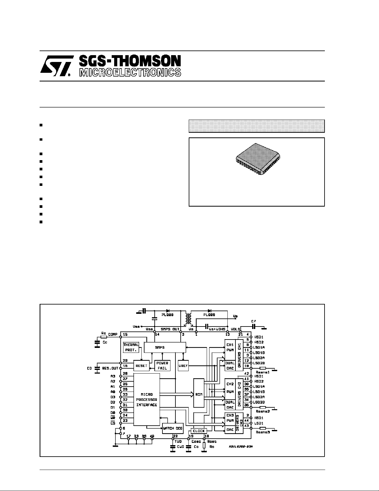
DESCRIPTION
TheL6280 is a multipowerdriver system for motor
and solenoid control applicatios that connects directly to a microprocessor bus. Realized in MultipowerBCD technology-- which combinesisolated
DMOS transistors, CMOS & bipolar circuits on the
BLOCK DIAGRAM
MULTIPOWERBCD TECHNOLOGY
PLCC44
ORDERING NUMBER: L6280
same chip -- it integrates two 1A motor drivers
(channels1 & 2) a 3A solenoid driver (channel 3)
and a 5V switchmode power supply.
All of the drivers in the L6280 are controlled by a
microprocessor which loads commands and
reads diagnostic information, treating the device
as a peripheral. Channels 1 and 2 feature a programmable output DMOS transistor configuration
that can be set during the initialization phase.
Thanksto very low dissipation of its DMOS power
stagesthe L6280 needs no heatsink and is packagedin a 44-leadPLCC package.
January1992
This is advanced information on a new product now in development or undergoing evaluation. Details are subject to change without notice.
1/26
L6280
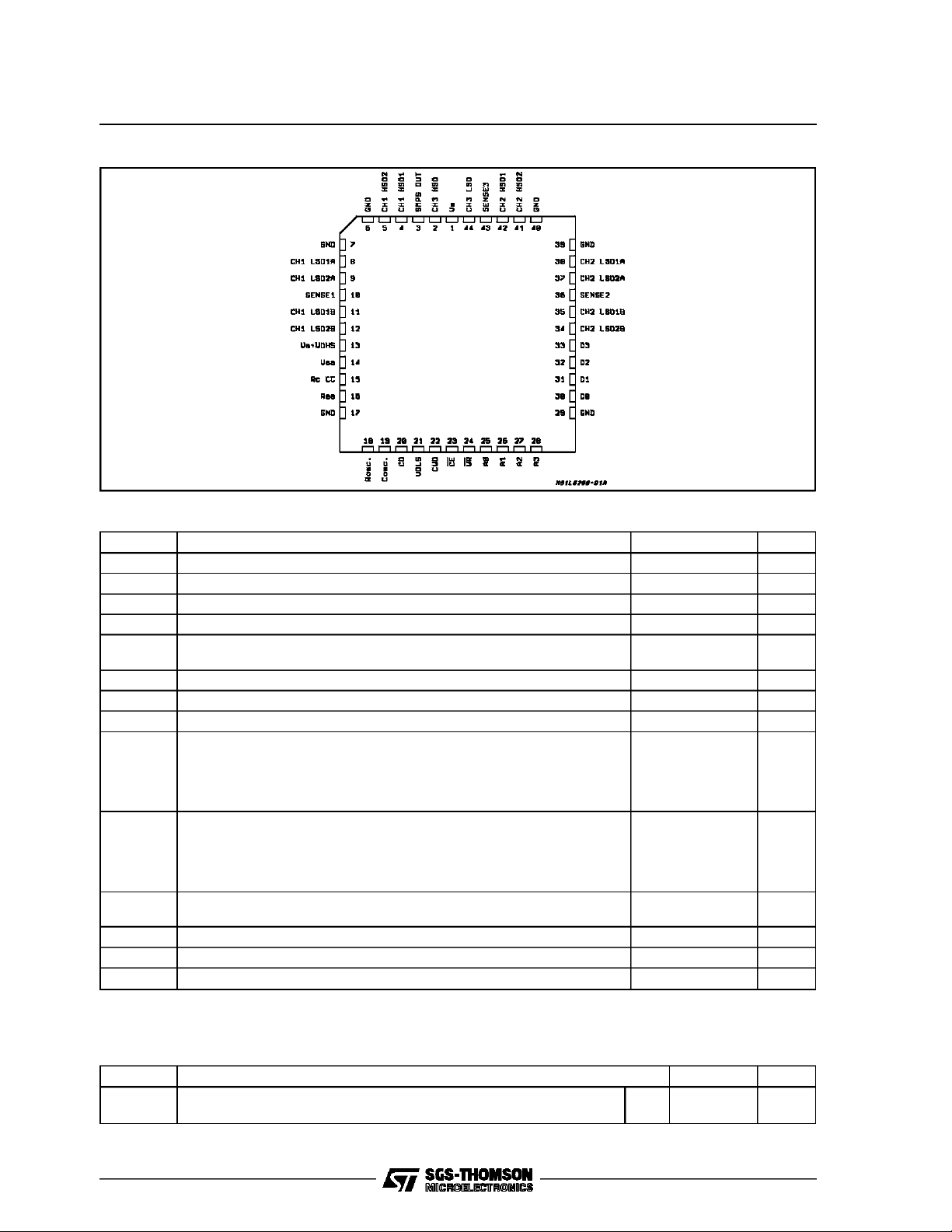
PIN CONNECTION (top view)
ABSOLUTE MAXIMUMRATINGS
Symbol Parameter Value Unit
V
V
SS
V13 Pin 13 InputVoltage (Note B) 60 V
V
DHS
V
V
OD
V
sense
V
I
LSD
I
HSD
I
SSOUT
I
RES
P
tot
T
stg;Tj
Notes: A) D0 =D1 = D2 = D3 =0; B) V13 = VS+V
D) D0 = 1; D1 = D2 = D3 = 0; E) D1 = 1; D0 =X; D2 =D3 = 0; F) The pulse width must be< 5ms and the Duty Cycle must be < 10%
G) The pulse widthmust be <5ms and the Duty Cyclemust be< 6%; H) mounted on board with minimized dissipatingcopper area.
THERMAL DATA
Power Supply Voltage (Note A) 35 V
S
Logic Supply Voltage 7 V
High Side Out Transistor Driving Voltage (NoteB,C) 18 V
Output Voltage. CH1; CH2: Unipolar Motor Drive (Note D)
O
CH3
60
60
Differential Output Voltage CH1; CH2; FullBridge Configuration (Note E) 60 V
Sensing Voltage -1 to 2 V
Logic Input Voltage -0.3to VSS+0.3 V
I
Low Side DriverInput Current
CH1; CH2 DC Operation
Peak (Note F)
CH3 DC Operation
Peak (Note G)
0.7
2
3
4.4
High Side Driver Onput Current
CH1; CH2 DC Operation
Peak (Note F)
CH3 DC Operation
Peak (Note G)
SMPS Output Current (Continuous)
(Peak; TON< 5ms)
1
2
3
4.4
1
2
Reset Output Open Drain Input Current 16 mA
Total Power Dissipation atTamb = 70°C (Note H) 1.6 W
Storage an Junction TemperatureRange -40 to 150 °C
; C) At 20V > V
DHS
> 17V the input current at pin 13 mustbe < 30mA;
DHS
V
V
A
A
A
A
A
A
A
A
A
A
Symbol Description Value Unit
R
th j-pins
R
th j-amb
(*) Mounted on board with minimized dissipating copper area.
Thermal Resistance Junction-pins
Thermal Resistance Junction-ambient (*)
Max.
Max.
12
50
2/26
°C/W
°C/W
PIN DESCRIPTION
PINS NAME FUNCTIONS
1V
S
2 HSD 1 High Side CH 3 Power Output
3 SMPS OUT Output of Switchmode Power Supply
4 HSD 1 High Side CH 1 Power Output
5 HSD 2 High Side CH 1 Power Output
6, 7,17,29,
GND Common GroundedTerminal
39, 40
8 LSD 1A Low Side CH 1 Power Output
9 LSD 2A Low Side CH 1 Power Output
10 SENSE 1 A Resistor Rsense, connected to this pinallows loadcurrent control for CH 1
11 LSD 1B Low Side CH 1 Power Output
12 LSD 2B Low Side CH 1 Power Output
13 V
14 V
S+VDHS
SS
15 Comp. An RC series network allows the compensation of the SMPS regulation loop
16 RES OUT The reset opendrain output can be used to warnthe microprocessor about V
18 R
19 C
20 C
21 V
22 t
OSC
OSC
D
DLS
WD
23 CS Enable Input(active when low)
24 WR Write Input. WhenWR is low the data is loaded into the µP interface
25 A0 Operation Selection (see programming sequence).
26 A1 Operation Selection (see programming sequence).
27 A2 Channel Selection (see programming sequence).
28 A3 Channel Selection (see programming sequence).
30 D0 Data (see programming sequence).
31 D1 Data (see programming sequence).
32 D2 Data (see programming sequence).
33 D3 Data (see programming sequence).
34 LSD 2B Low Side CH 2 Power Output
35 LSD 1B Low Side CH 2 Power Output
36 SENSE 2 A Resistor R
37 LSD 2A Low Side CH 2 Power Output
38 LSD 1A Low Side CH 2 Power Output
41 HSD 2 High Side CH 2 Power Output
42 HSD 1 High Side CH 2 Power Output
43 SENSE 3 A Resistor R
44 LSD 1 Low Side CH 3 Power Output
Power Supply Voltage Input
Input Voltage for the HSD Gates Drive
Logic Supply Voltage Input
and VSSstatus
Together with C
Together with C
, sets the cycle time ofthe SMPS t = 1.1 ROC
OSC
, sets the cycle time ofthe SMPS t = 1.1 ROCOand sets the
OSC
minimum ON time in the PWM current control loop
The value of this capacitor sets the reset delay tD=7 x10⁴C
D
By-pass Capacitorof the LSD Gates Voltage drive
ThevalueofthisCWDsetsthedurationofthewatchdogmonostable tWD=3x 10⁴CWD.
If no watchdog signal is generatedinto the TWD timethe device is automatically
switched off.
, connected to this pin allows load current control forCH 2
sense
, connected to this pin allows load current control forCH 3
sense
L6280
S
O
3/26
L6280
ELECTRICALCHARACTERISTICS (VS= 20V; Tj=25°C; VSS =5V; V
C
=680pF; unlessotherwise specified)
O
=15V; RO=165KΩ;
DHS
Symbol Parameter Test Condition Min. Typ. Max. Unit
I
DSS
V
s
V
INL
I
INL
V
INH
I
INH
V
ROUT
V
PF
I
S
V
SS
I
SS(IN)
I
SS(OUT)
f
osc
f
1
f
1max
f
2
f
3
Leakage Current Fig. 1 VDS = 60V 2 mA
Power Supply Voltage Note 1,2 >V
PF
48 V
Low Level InputVoltage -0.3 1.35 V
Low Level InputCurrent -10 µA
High Level InputVoltage 3.15 VSS V
High Level Input Current 10 µA
Low Level Reset Out I16 = 1.5mA 0.8 V
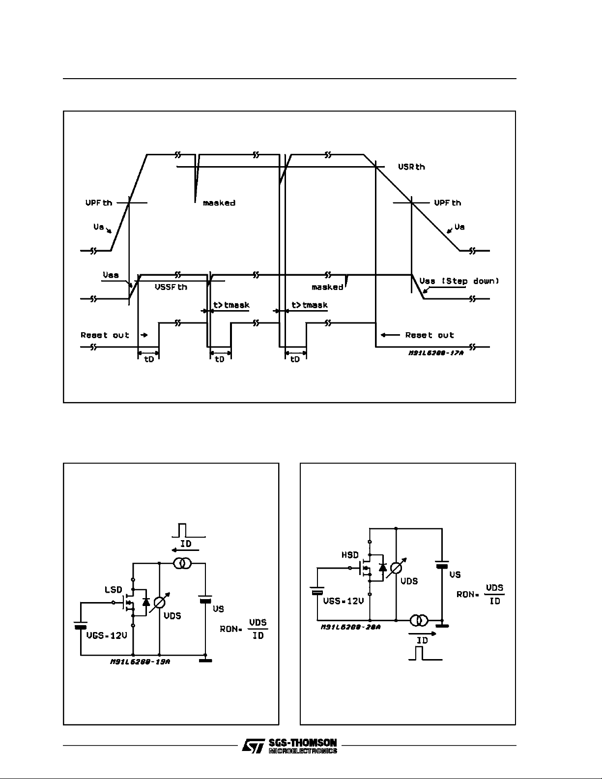
Power Supply Fail Voltage (Fig. 2) 13 V
Quiescent Supply Current VS = 12V 4.5 6 7.5 mA
Logic Supply Voltage 4.75 5 5.25 V
Logic Supply Current 4.5 6 7.5 mA
SMPS Out Current Range Note 3 800 mA
Oscillator Frequency 64 80 96 KHz
SMPS and CH3 Frequency f
osc
Max SMPSSwitching Frequency 120 KHz
PWM Frequency fosc/2 KHz
High Side Driver Switching
fosc/4 KHz
Frequency
TSD Thermal Shutdown 125 150 °C
t
WD
t
D
R
ON
Monostable Watchdog Time CWD = 0.22µF (Note 4) 6.6 ms
Reset Delay Time CD= 0.22µF; Fig.2 (Note 5) 15.4 ms
ON State DrainResistance
Transistor LSD CH1 - CH2
HSD CH1 - CH2
LSD CH3
HSD CH3
SMPS
Fig 3; 4ab
2
1.1
0.5
0.5
1
2.4
1.4
0.8
0.8
1.2
SENSE Internal Sense LOW-Pass Filter 300 500 ns
V
ref
DAC Reference Voltage D0=D1=D2 =1 (Table 1) 1 V
DAC DAC Resolution (3 Bit) (See Table 1) Vref/8 V
t
C
Discarge Time of Cosc
(Note 6) 0.4 µs
Capacitor (Minimum TON)
V
DHS
I
DHS
I
SS (OUT) max
HSD Gates Voltage Drive 13 15 17 V
Pin 13 OverageInput Current 3 mA
SMPS Overload Protection
1.2 A
Current
V
DLS
V
SSF
V
FHSD (1;2)
Pin 21 OverageInput Voltage 12 V
Logic VSS FailThreshold Voltage (Fig. 2) 2.6 4.1 V
Internal Clamp Diode Forward
@IDS = 0.4A (Fig. 5) 1.2 V
Voltage CH1/CH2
V
FLSD
(1AB;2AB)
V
FHSD
Internal Clamp Diode Forward
Voltage CH1/CH2
Internal Clamp Diode Forward
@IDS = 0.4A (Fig. 5) 1.4 V
@IDS= 1A (Fig. 5) 1.1 V
Voltage CH3
KHz
Ω
Ω
Ω
Ω
Ω
4/26

ELECTRICALCHARACTERISTICS (continued)
Symbol Parameter Test Condition Min. Typ. Max. Unit
V
FLSD
Internal Clamp Diode Forward
Volt. CH3
t
CW
t
WPW
t
SU
t
DH
t
WC
Notes:
1) When driving a unipolar stepper motor the Power Supply Voltage must be lower than24V.
2) A lower Supply Voltage than the Power Fail thresholddisables the Step Down Power Supply (see Fig.2)
3) The minimumoutput current equals the half of the peak-to-peak current ripple
4) t
WD ≅ CWD
5) t
x 3.5 /50 x 10
D ≅ CD
6) t
C≅ COSC
Chip Seletion to End of Write (Fig. 6) 700 ns
Write Pulse Width (Fig. 6) 700 ns
Data Set-up Time (Fig. 6) 700 ns
Data Hold-up Time (Fig. 6) 0 ns
Write Cycle Time (Fig. 6) 2.7 ms
x 1.5 /50 x 10
x R
(sec); R
int.
-6
(sec)
-6
(sec)
= 600Ω ± 30%
int.
@IDS= 1A (Fig. 5) 1.1 V
L6280
Figure1: DrainLekage Current Equivalent Test
Circuit. The Gate-to-Source Voltage
VGS is below theSwitch-Off
Threshold.
Figure3: TypicalNormalized R
JunctionTemperature
DS(ON)
vs.
5/26
L6280
Figure2: Reset Output Behaviour versusPower Supply Voltage V
and/orLogic SupplyVoltage VSS.
S
Figure4a:Sink Output DMOSRONEquivalent
Test Circuit
Figure4b:Source OutputDMOS R
Test Circuit
Equivalent
ON
6/26
Figure5: Possible HardwareConfigurationsof PowerStage (CH1and CH2)
L6280
Figure6: Write Cycle
7/26
L6280
SYSTEM DESCRIPTION (Refer to the Block Dia-
gram)
The L6280 is a single chip power microsystem
which includes drives for three differentloads, the
associated control logic and a Switched Mode
PowerSupply(SMPS) at V
=5V± 5%.
SS
The IC can be directly connected to a standard
microprocessor because of its common I/O interface architecture. The L6280 can exchange information regarding the load driver and the control
methodvia a 8 bit data bus. The blocknamed microprocessor interface decodes the first four bits
(A0....A3),which, depending on the content of the
remainingfour(D0.......D3)are used to enable the
power DMOS, to activate the PWM loop, and finally to set the D/A output value.
The power stage can be divided into 3 channels.
Channels1 and 2 have 6 DMOS transistors each
one (2high side drivers with R
drivers with R
=2Ω). Depending on the appli-
dson
=1Ω, 4 low side
dson
cation load, these driver transistors can be connected in different ways. The microprocessor, via
software, must activate the proper control loop to
optimize operation of different loads and output
stage configurations. Because of this programmability in the control of the output configurations,
a large variety of different loads can be driven by
the same integrated circuit (see possible configuration for power stage on Figure 5) giving the
greater system flexibility. Current levels up to 1A
are possible from CH1 and CH2, limited primarily
by the power dissipation of the IC.
The third channel has a fixed configuration intended to drive a solenoid. DMOS transistorswith
0.5Ω R
are used to provide 4A max load ca-
dson
pability.
All three channels have 3 bit current D/A resolution. Some auxiliary blocks of diagnostic and protection(e.g.: Thepower Fail/Reset andthe watchdog) are provided to protect the system from
microprocessorfailure or powerfail.
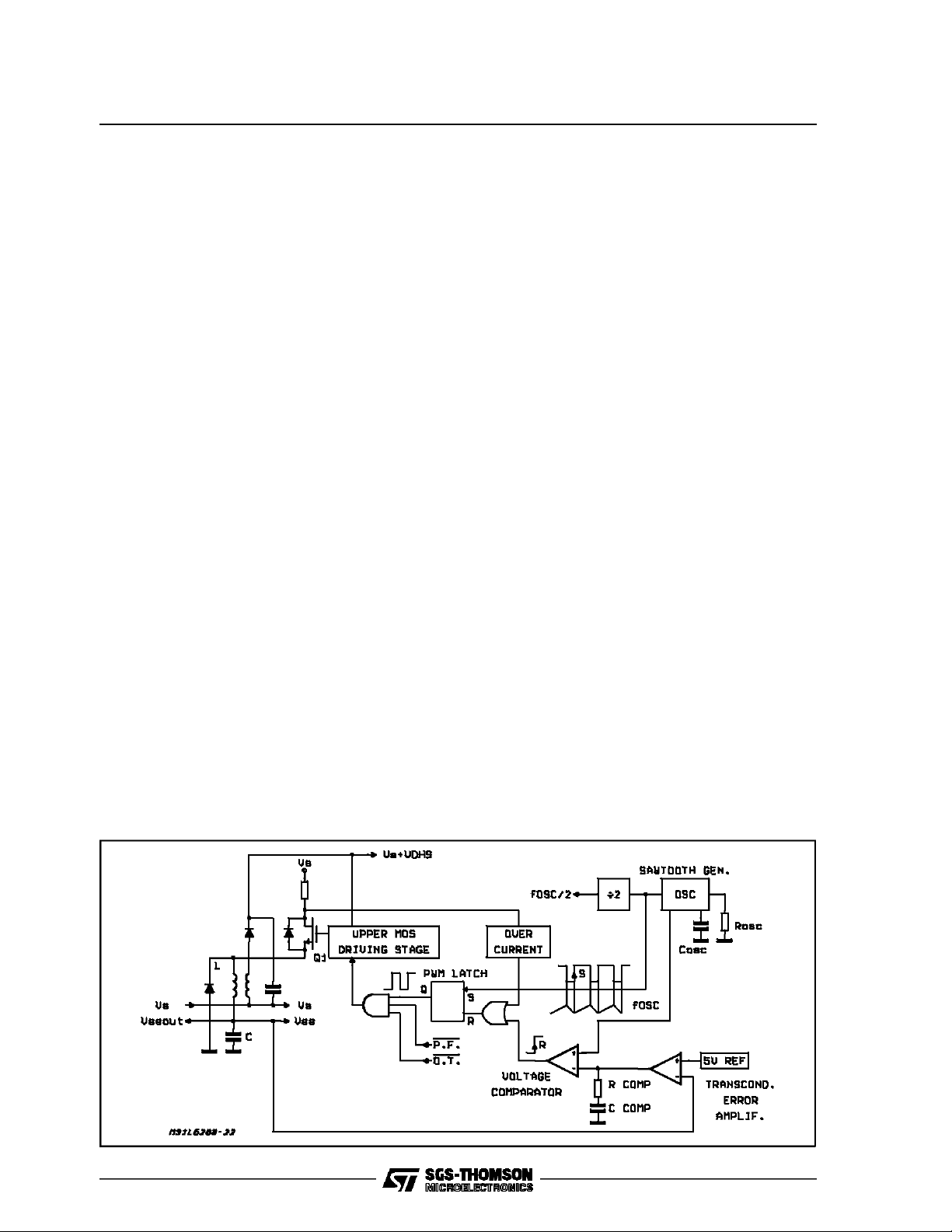
Figure7: SMPSBlock Diagram
Step Down Switchmode Power Supply (See
Figure7).
The step down switchmode power supply con-
tains a DMOS power stage with 1Ω R
dson
(Q1),
control circuitry, diagnostics and protection circuits; a regulated voltage (V
is used to drive
SSout)
some of the internal circuit blocks and the external microprocessor and memories. Thanks to the
DMOS output stage this regulator can deliver a
continuousoutput power of 4W (5V; 0.8A) with an
efficiency betler than 90% at a typical frequency
of80kHz.
The regulation loop uses a classical pulse width
modulation circuit that includes a sawtooth generator,an erroramplifier,a voltagecomparatoranda
PWM latch. A precision 5V referenceis generated
and trimmed on chip to guaranteea 5% tolerance.
This referenceis used as voltage referencefor the
SMPSand the reference for the DACs.
The IC also provides an extra voltage (V
S+VDHS
for the correct driving of the high side drivers.
These transistors require a gate voltage higher
than the supply voltageVs to obtainthe minimum
ON resistance. Because of the v ery low current
needed to drive DMOS transistors, this auxiliary
voltage is easily obtainedfrom a second winding
on the inductor of the LC output network (see ApplicationInformation).
An overcurrent protection circuit is included to
turn OFF the power transistor when a current
levelof 1.2A isexceeded.
The SMPS block also includes a voltage sensing
circuitto generate a powerON reset signal for the
microprocessor. This Power Fail circuit senses
the input supply voltage and the output regulated
voltage and sets the Reset-out pin to the high
voltage only when both the sensed voltages are
correct.
Finally, the SMPS block is able to deliver f
OSC/2
used in the actuation stage for the PWM control
of the current(CH1; CH2 and CH3).
)
8/26
 Loading...