

L6270
90V BCD MIXEDTECHNOLOGY
SO24AND SO20 PLASTICSMDPACKAGE
4.5 TO 13.2V OPERATIVEVOLTAGE
±25 TO ±40V OUTPUT VOLTAGE RANGE
SELECTABLEBY EXTERNALRESISTOR
FULL-WAVE RESONANT DC-DC CON-
VERTER USING SINGLE COIL FOR DUAL
HIGH VOLTAGE GENERATOR WITH OUTPUT SLEW RATE CONTROL AND SELF
CURRENTLIMITING
LINEARMODE AND BANG-BANGMODE
±40VOR 0/+80VOPERATIVEVOLTAGE
DRIVINGCONFIGURATION MODES:
1.SINGLEENDEDVOLTAGE MODE
2.DIFFERENTIAL VOLTAGE MODE
3.SINGLEENDEDCHARGE MODE
DOUBLEOPERATIONAL AMPLIFIERS WITH
500KHZ GAIN BANDWIDTH PRODUCT AND
LOAD DRIVING CAPABILITY FROM 0.4NF
UP TO24NF
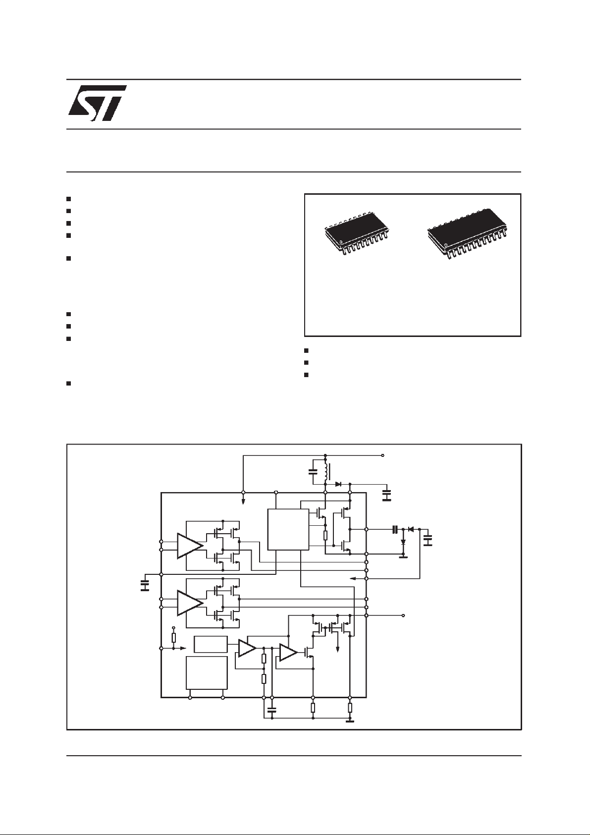
BLOCK DIAGRAM
L6271
MILLI-ACTUATORDRIVER
PRODUCT PREVIEW
SO20 SO24
ORDERING NUMBERS:
L6270 L6271
2.5V VOLTAGEREFERENCE
2.5V ANALOGSHIFTINGCIRCUITRY
POWERSAVING SLEEP MODE
DESCRIPTION
The L6270/1is a piezoelectricactuator driver.
RC
SLEEP
INB-
INB+
COMP
INA-
INA+
HVP
17
-
16
+
HVM
22
HVP
8
-
9
+
HVM
2.5V
50KΩ
7
REFERENCE
SLEEP
ANALOG LEVEL
SHIFTER
VOUT=VIN-2.5
VOUT VIN
V-SHIFTED VIN0-5
CRES
V512-AP COIL HVP
POWER
SUPPLY
1
1
1
1
BAND-GAP
1110
BANG-LIN
K
CONTROLLER
K
K
K
+
-
GND-A VREF
Vfdb
RESONANT
DC-DC
STEP-UP
100µA
+
-
1312
100nF 25KΩ
32120 24
1Ω
INTERNAL
CURRENT
BIAS
14
IREF
COIL
200µA
18
19
23
6
5
20
15
DC2REF
RREFDC
+40V
HBRIDGE1
GND-P2
OUTK-B
OUT1-B
HVM
OUTK-A
OUT1-A
V512A
VSUPPLY
4.5V-13V
100nF
VSUPPLY
D98IN959A
-40V
100nF47nF
February 1999
This is preliminary information on a new product now in development. Details are subjectto change without notice.
1/10
L6270 - L6271
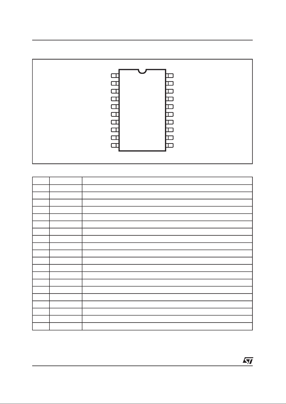
PIN CONNECTION(SO20)
H-BRIDGE
GND-P
COIL
OUT1-A
OUTK-A
SLEEP
INA(inv)
INA(not inv)
GND-A DC2ref
Vref Iref
2
3
4
5
6
7
8
9
10
D98IN968
20
19
18
17
16
15
14
13
12
11
PIN FUNCTIONS(SO20)
N. Name Description
1 H-BRIDGE 40V Half Bridge output for negative charge pump.
2 GND-P Power ground.
3 COIL Coil for positive step up.
4 OUT1-A Output ampl.A.
5 OUTK-A Hi current output ampl.A.
6 SLEEP Sleep mode for stand-by condition(1=SLEEP 0=operative).
7 INA (inv) Inverting input of A-amplifier.
8 INA (not inv) Non Inverting input of A-amplifier.
9 GND-A Analog ground.
10 V
11 I
12 DC2ref Reference voltage for DC-DC converter X20.
13 INB (not inv) Non Invertinginput of B-amplifier.
14 INB (inv) Inverting input of B-amplifier.
15 OUTK-B Hi current output ampl.B.
16 OUT1-B Output ampl.B.
17 V512-AP Analog&Power voltage supply 5 to 12V.
18 RC comp DC-DC converter compensation network.
19 HVM Negative High voltage generated op amp supplier.
20 HVP Positive High voltage generated op amp supplier.
ref
ref
Precise 2.5V reference voltage.
External resistor for precise internal current reference.
HVP1
HVM
RC comp
V512-AP
OUT1-B
OUTK-B
INB(inv)
INB(not inv)
2/10
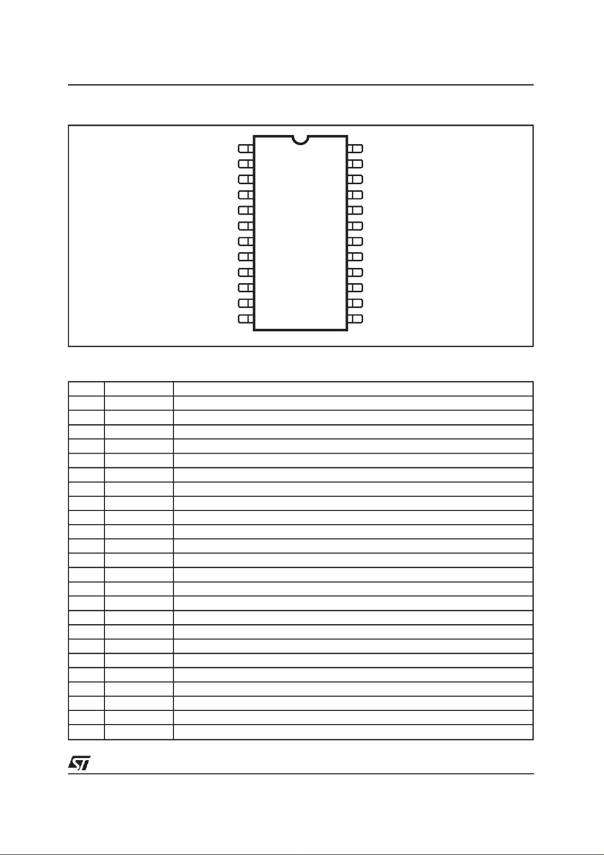
PIN CONNECTION(SO24)
L6270 - L6271
H-BRIDGE
GND-P
COIL
N.C.
OUT1-A
OUTK-A
SLEEP
INA(inv)
INA(not inv) INB(not inv)
V-SHIFTED DC2ref
2
3
4
5
6
7
8
9
10
24
23
22
21
20
19
18
17
16
15
HVP1
HVM
RC comp
LIN/BANG
V512-AP
OUT1-B
OUTK-B
INB(inv)
Vin 0-5 Iref11 14
1312GND-A Vref
D98IN969
PIN FUNCTIONS(SO24)
N. Name Description
1 H-BRIDGE 40V Half Bridge output for negative charge pump.
2 GND-P Power ground.
3 COIL Coil for positive step up.
4 N.C.
5 OUT1-A Output ampl.A.
6 OUTK-A Hi current output ampl.A.
7 SLEEP Sleep mode for stand-by condition (1=SLEEP 0=operative).
8 INA (inv) Inverting input of A-amplifier.
9 INA (not inv) Non Inverting input of A-amplifier.
10 V-SHIFTED Analog level shifter output Vin-Vref (-2.5 to +2.5 dynamic range)
11 Vin 0-5 Input positive voltage
12 GND-A Analog ground.
13 V
14 I
ref
ref
15 DC2ref Reference voltage for DC-DC converter X20.
16 INB (not inv) Non Inverting input of B-amplifier.
17 INB (inv) Inverting input of B-amplifier.
18 OUTK-B Hi current output ampl.B.
19 OUT1-B Output ampl.B.
20 V512-AP Analog&Power voltage supply 5 to 12V.
21 LIN/BANG Linear or Bang-bang select pin (V512 = BANG 0 = Linear)
22 RC comp DC-DC converter compensation network.
23 HVM Negative High voltage generated op amp supplier.
24 HVP Positive High voltage generated op amp supplier.
Precise 2.5V reference voltage.
External resistor for precise internal current reference.
3/10

L6270 - L6271
ABSOLUTEMAXIMUM RATINGS
Symbol Parameter Value Unit
V512 Supply voltage pin 20 referredto Ground 14 V
HVP Positive high voltage referred to HVM 84 V
HVM Negative high voltage referred to Ground -42 V
IN A&B Amplifier input voltage common mode ±6V
o to 5 Level shifts input voltage -0.5 to +5.5 V
Vi
n
T
amb
T
stg
All the voltagevalue are referred to ground.
Operative Ambient Temperature -20 to +80 °C
Storage Temperature -40to +125 °C
ELECTRICAL CHARACTERISTICS
(All the following parameters are specified @ 27°C and V512 =
12V, unless otherwisespecified.)
Symbol Parameter Test Condition Min. Typ. Max. Unit
V
512
HVP
HVM Output negative voltage -40 -25 V
HVripple HVP,HVM ripple External filter cap. 100nF
DC-DC gain Ratio of HVP and DC-DC ref.
I, hvp Output current (see figure 1a)
I, hvm
T
op
F
switch
R
ds,on
I
boost
CP-slope Charge Pump Slope 150 V/µs
I
sleep
V
ref
I
vref
V
ref, cap
I
ref, res
V
sup
DC gain OpAmp DC gain 130 dB
GBW OpAmp Gain Bandwidth
DCinp OpAmp Input dynamic voltage Double supply -5 5 V
DC-DC
OFF
Main power supply 4.5 13.2 V
(1)
Output positive Voltage Double Supply Voltage 25 40 V
Single Supply Voltage V
Single Supply Voltage V
512
512
≥ 8
≤ 8
30
25
Bang-BangMode
Linear Mode
19 20 21
voltage PIN15
Time to operating condition 5 ms
(2)
Switching Frequency 80 550 kHz
Boost transistor ON resistance 4
Boost transistor current limiting 700 mA
Total current in sleep mode 1 mA
Reference voltage at PIN13 2.4 2.5 2.6 V
Reference voltage output
-1 1 mA
current
Filter capacitor at PIN13 10 100 nF
Resistor at PIN14 for precise
25 k
internal current (100µA)
Minimum OpAmp supply
Voltage (HVP if externally
given)
Double Supply V512
+4
Single Supply V512
+4
product
Cload 0.4nF to 24nF
Double Supply Voltage
500 KHz
Single supply 1.2 10 V
DC-DC Converter switched-off
when DC
2
REF voltage lower
than
80
40
2.5
0.8
0.6 V
V
V
V
V
Ω
Ω
V
V
4/10

L6270 - L6271
ELECTRICALCHARACTERISTICS
(continued)
Symbol Parameter Test Condition Min. Typ. Max. Unit
V
DC, I
out
OpAmp Output dynamic voltage Capacitive load HVM HVP V
OpAmp Bias supply current
bias
7mA
(both)
I
out
PSRR,P OpAmp Positive power supply
OpAmp Dynamic Output current -75 75 mA
@ 50kHz TBD dB
rejection ratio
PSRR,N OpAmp Negative power supply
@ 50kHz TBD dB
rejection ratio
C
load
OpAmp Load capacitance
Voltage mode Gain min 20dB 0.4 24 nF
range
C
int
K OpAmp Current ratio
OpAmp Integration capacitance Charge mode Gain min 20dB 0.4 24 nF
9.8 10 10.2
OUTK/OUT1
(3)
DC
I
err
V
offset
Shift range
OpAmp Ioutk Iout1 = 0 -10 50 µA
OpAmp Input offset voltage
Dynamic Shifter
14V
10 mV
±
Input Range
Note 1: Selectableby externalresistor.
Note 2: Setby external Coil and Capacitor.
Note 3: Itwill be write after silicon characterization, it’s designed for a maximum offset of a few mA.
Incharge mode the Piezo isin openloop, andif Cpiezo= 0.4nF witha maximum Current error of ±5µA the Maximum long time voltage
driftis ±12mV/µs
Figure 1a. HVP load regulation in single supply
mode”.
V
S
(V)
38
36
34
32
30
28
26
24
22
0 0.004 0.008 0.012 0.016 IL(A)
Supply=8V
Supply=5V
D99IN1003
5/10

L6270 - L6271
Figure 1. Charge Mode Configuration (only a suggestion,the applicationis completelyfree
accordingwith ElectricalCharacteristics).
Qpiezo=K*[Cint*(1+Ra/Rb)+C]*Vdac
Qpiezo=Cost*Vdac
HVP
1
Cost=k*[Cint*(1+Ra/Rb)+C]
K
Rb
C
+
-
HVM
Ra
1
Vdac
OPERATIONALAMPLIFIERS DESCRIPTION
Each driver has two output stages scaled in current by a factorK = 10.
In voltage mode configuration the two outputsare
shorted.
In charge mode configuration OUT1 drives a capacitor Cint and is closed in feedback, while
OUTK drives the piezo, mirroring the current supplied to Cint, with a current multiplied by a K factor (see Fig.1).
The supply voltage can be internally generatedby
the DC-DCconverter,or external, maintainingthe
DC-DC converter in sleep mode (PIN15 shorted
to ground), in this case the supply voltage can be
0 to V512+4 minimum value up to 80V in single
supply or V512+4 to 40V symmetricalto ground.
The drivers have 130dB DC gain and the Bandwidth is 500KHz. Stability is granted with a minimum gain of 20dB, for a capacitive load in the
range 0.4nF up to 24nF.
The driverscan be supplied with HVP-HVM (double supply mode) or with HVP-Ground (single
supply mode). In both cases they can achieve a
rail-to rail output dynamic range with a maximum
load currentof ±75mA.
In double supply mode the input stage has 5V/+5V dynamic range, while in single supply
modeit has1.2V up to 10V input dynamicrange.
A 2.5V internal reference voltage is available at
one pin (Vref) thatcan be used to close the feedback if the input signal is symmetrical around
2.5V.
In this case the output dynamic is symmetrical
around 2.5V. It is present a 2.5V down level
shifter that can be connected between the input
signal and the input of the opamp, to work inter-
Cpiezo
K
Cint
D98IN970A
R
P
nally with a signal symmetricalto ground.
DC-DC CONVERTER DESCRIPTION
The DC-DC converterinside the chip can be supplied from 5V up to 12V andhas two parts, one to
supplythe positiveand one to supply thenegative
voltage.
The positiveone takes the reference from the pin
2
REF and multiplies it by 20 to have the output
DC
voltage.
2
If DC
REF is lessthan 0.6Vthe whole DC-DC converter is shut down and the high voltages have to
be supplied from external. In Sleep Mode (sleep
pin) HVM is shorted to GND. When in singlesupply,no loadhas to be connectedto H-bridge output
andHVM mustbe connectedto GND.
The topology is a standard resonant full-wave
boost one: the LC oscillation is kept running all
the time and a set of comparatorsis used to synchronize turning on and off of the power MOS in
order to have zero current and zero voltage
switchingand furthermorecontrolledrectification.
The step-up converter is designed to work in
”Bang-Bang” mode and in Linear mode, in this
case an AC compensation network is required
(RC-comp)to guaranteethe stabilityin a wide operative range (i.e. changing coil, load, output and
input voltage...).
Bang-Bangmode
In
(Bang/Lin=V512high condition) whenever the output HVP goes down fixed
threshold(Vt
=20⋅DC2REF),the next oscilla-
h,out
tion phase is more powerful and is used to transfer energy from the powersupply to the output.
Linear mode
In
, according to the ouput voltage,
the current loaded into the coil is changing like a
6/10

L6270 - L6271
Voltage Loop-Current Controlled system, and in
every pulse there is a regulated power transfer to
the load.
The resonantLC topology has been chosenin order to limit the voltage slew-rate across the coil
within reasonable values and so, to minimize irradiation problems.
The negative converter is a simple charge transfer: it is supplied by the positive high voltage and
it capacitively translates this positive voltage
Figure 3. DC-DC converter
HVP
BACK-UP
V512
OSCILL.
+
-
200µA
L
DC-DC
LOGIC
B
:5
L
2.5V
down to a negative one, obviously to limit irradiation problems also the chargeoutput has a limited
slew-rate; moreover to reduce intermodulation
phoenomenasthe charge output is synchronized
with the LC oscillationsof the resonant boost.
This negative voltage is (not counting drops on
external rectification diodes) in tracking with the
positive one and so the negativeoutput controller
is notrequired.
V512
V512
+
-
+
-
+
-
R
S
HVP
+40V
HVM
-40V
D98IN971A
7/10

L6270 - L6271
DIM.
MIN. TYP. MAX. MIN. TYP. MAX.
A 2.35 2.65 0.093 0.104
A1 0.1 0.3 0.004 0.012
B 0.33 0.51 0.013 0.020
C 0.23 0.32 0.009
D 12.6 13 0.496 0.512
E 7.4 7.6 0.291 0.299
e 1.27 0.050
H 10 10.65 0.394 0.419
h 0.25 0.75 0.010 0.030
L 0.4 1.27 0.016 0.050
K0°(min.)8°(max.)
mm inch
0.013
OUTLINE AND
MECHANICAL DATA
SO20
8/10
B
e
D
1120
110
L
hx45°
A
K
A1
C
H
E
SO20MEC

L6270 - L6271
DIM.
MIN. TYP. MAX. MIN. TYP. MAX.
A 2.35 2.65 0.093 0.104
A1 0.10 0.30 0.004 0.012
A2 2.55 0.100
B 0.33 0.51 0.013 0.0200
C 0.23 0.32 0.009
D 15.20 15.60 0.598 0.614
E 7.40 7.60 0.291 0.299
e 1.27 0,050
H 10.0 10.65 0.394 0.419
h 0.25 0.75 0.010 0.030
k0°(min.),8° (max.)
L 0.40 1.27 0.016 0.050
mm inch
0.013
OUTLINE AND
MECHANICAL DATA
SO24
0.10mm
.004
Seating Plane
1
A2
A
Be
A1
K
D
1324
E
12
hx45°
L
A1 C
H
SO24
9/10

L6270 - L6271
Information furnished is believed to be accurate and reliable. However, STMicroelectronics assumes no responsibility for the consequences
of use of such information nor for any infringement of patents or other rights of third parties which may result from its use. No license is
granted by implication or otherwise under any patent or patent rights of STMicroelectronics. Specification mentioned in this publication are
subject to change without notice. This publication supersedes and replaces all information previously supplied. STMicroelectronics products
are not authorized for use as critical components in life support devices or systems without express written approval of STMicroelectronics.
The ST logo is a registered trademark of STMicroelectronics
1999 STMicroelectronics – Printed in Italy – All Rights Reserved
STMicroelectronics GROUP OFCOMPANIES
Australia - Brazil - Canada - China- France - Germany - Italy - Japan - Korea - Malaysia - Malta - Mexico - Morocco - The Netherlands -
Singapore- Spain - Sweden - Switzerland - Taiwan - Thailand - United Kingdom - U.S.A.
http://www.st.com
10/10
 Loading...