

L6268
12VDISK DRIVE SPINDLE& VCM, POWER
& CONTROL“COMBO”
PRODUCT PREVIEW
GENERAL
12V (+/- 10%) OPERATION.
REGISTERBASEDARCHITECTURE
MINIMUMEXTERNAL COMPONENTS
BICMOS+ VERTICALDMOS (1.5mm)
VCM DRIVER
1.5ADRIVE CAPABILITY
0.9WTOTALBRIDGE IMPEDANCEAT 25°C
LINEARMODE
PHASESHIFT MODULATION(PWM MODE)
INSTANTANEOUS, (GLICH FREE) SWITCH
BETWEENTHE 2 MODES
CLASS ABOUTPUTDRIVERS
ZEROCROSSOVERDISTORSION
14 BIT DAC DEFINE OUTPUTCURRENT
SELECTABLETRANSCONDUCTANCE
4 PROGRAMMABLEPARKINGVOLTAGE
DYNAMICBRAKE
SPINDLEDRIVER
2.0ADRIVE CAPABILITY
0.8WTOTALBRIDGE IMPEDANCEAT 25°C
BEMF, INTERNAL OR EXTERNAL, PROC-
ESSING
SENSOR-LESSMOTOR COMMUTATION
PROGRAMMABLE COMMUTATION PHASE
DELAY
LINEARMODE AND CONSTANT TOFF PWM
OPERATIONMODE
INTERNAL FREQUENCY LOCKED LOOP
SPEEDCONTROL (FLL)
BEMFRECTIFICATIONDURING RETRACT
BUILT-INALIGNAMENT&GOSTART-UP
INDUCTIVE SENSINGSTART UP OPTION
RESYNCHRONIZATION
DYNAMIC& REVERSEBRAKE
CONTROLLABLEOUTPUTSLEW RATE
OTHER FUNCTIONS
12V AND 5V MONITORINGWITH EXTERNAL
SET TRIP POINTSANDHYSTERESIS
POWERUP/DOWN SEQUENCING
BICMOS TECHNOLOGY
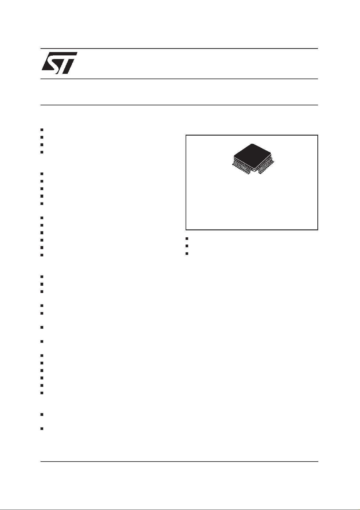
TQFP44 (10x10mm with slug)
ORDERING NUMBER: L6268
LOW VOLTAGESENSE
3.3V INPUT LOGICCOMPATIBILITY
THERMAL SHUTDOWN AND PRETHERMAL
WARNING
DESCRIPTION
The L6268 integrates into a single chip both spindle and VCMcontrollers as well as power stages.
The device isdesigned for 12V diskdrive application requiring up to 2.0A of spindle and 1.5A of
VCM peak currents.
A serialport with up to25 MHz capabilityprovides
easy interface to the microprocessor. A register
controlled Frequency Locked Loop (FLL) allows
flexibility in setting the spindle speed. Integrated
BEMF processing, digital masking, digital delay,
and sequencing minimize the number of external
componentsrequired.
Power On Reset(POR) circuitry is included.Upon
detection of a low voltage condition, POR is asserted, the internal registers are reset, and spindle powercircuitryis tri-stated.The BEMF is rectified providing power for actuator retraction
followed by dynamicspindlebraking.
The device is built in BICMOS technology allowing dense digital/analog circuitry to be combined
with a highpower DMOS outputstage.
April 1999
This is preliminary information on a new product now in development. Details are subject to change withoutnotice.
1/17
L6268
BLOCK DIAGRAM
CS
SW1
SDATA
SCLK
SDEN
TR_12V
TR_5V
CP
CHARGE
PUMP
ISO
DRIVER
SERIAL
INTERFACE
SUPPLY
FAULT
MONITORS
POR_DELAY
PORB
FLL_RES
FLL_FILTER
INDEX
FREQUENCY
LOCK LOOP
START-UP
REGISTERS
THERMAL
SUPPLY
VDD
GND
SYS_CLK
DGND
FCOM
SPINDLE SEQUENCER
RE_SYNC
DYNAMIC/
REVERSE
BRAKE
VCM
CURRENT
CONTROL PSM/LIN
VCM
CALIBRATION
14 BIT
VCM DAC
REFERENCE
GENERATOR
DAC
SPN_COMP
PROCESSING
ZERO CROSS
VOLTAGE
V12/2
BRK_CAP
PWM/SLEW
BEMF
DETECTION
SPINDLE
CURRENT
CONTROL
PWM/LIN
PARKING
BEMF
RECTIFICATION
VCM_CAL
ERROR_IN
+
-
A
B
C
A+
A-
-
A=4
+
SENSE_OUT
ERROR_OUT
VCC
OUT_A
CTAP
OUT_B
RSENSE
OUT_C
ISENSE
VCM_A+
VCC
VCM_AVCM_GND
SENSE_INSENSE_IN+
D99IN1042
PIN CONNECTION
2/17
FCOM
CTAP
PWM/SLEW
OUT_C
I_SENSE
R_SENSE
OUT_B
GND
R_SENSE
OUT_A
INDEX
SPN_COMP
VCC
AGND
DAC
ERROR_IN
TR-12V
ERROR_OUT
SENSE_OUT
44 43 42 41 3940 38 37 36 35 34
1
2
3
4
5
6
7
8
9
10
12 13 14 15 16
VCC
BRK_CAP
DGND
SDEN
SYS_CLK
171118 19 20 21 22
VDD
SCLK
SDATA
POR_DELAY
TR_5V
PORB
V12/2
VCM_CAL
FLL_FILTER
33
32
31
30
29
28
27
26
25
24
23
D98IN847
SW1
FLL_RES
VCC
VCM_A+
SENSE_INVCM_GND
SENSE_IN+
VCM_AVCC
CS
CP
PIN DESCRIPTION(Pin Types:D = Digital,P = Power,A = Analog)
N. Name Function
1 FCOM Output of the Spindle zerocross or Current Sense circuit.
2 CTAP Spindle Central Tap used for differential BEMF sensing.
3 PWM/SLEW RC network sets the Spindle LinearSlew Rateand PWM OFF-Time.
4 OUT_C Spindle DMOS Half BridgeOutput and Input C for BEMF sensing.
5 I_SENSE Input to sense the voltage the SPINDLE Sense Resistor.
6 R_SENSE Output connection for the Motor Current Sense Resistor to ground.
7 OUT_B Spindle DMOS Half Bridge Output and Input B for BEMF sensing.
8 GND Spindle Ground (Substrate).
9 R_SENSE Output connection for the Motor Current Sense Resistor to ground.
10 OUT_A Spindle DMOS Half BridgeOutput and Input A for BEMF sensing.
11 INDEX Input to allow Spindle to be locked to Index (servo) pulse.
12 BRK_CAP Storage Capacitor for brake circuit. typically 5.9V.
13 VCC +12V Power Supply for Spindle Power section.
14 DGND Digital Ground.
15 SYS_CLK Clock Frequency for system timers and counters.
16 SDEN Serial DataEnable. Active high input pin for the serialport enable.
17 SDATA Serial Port Data. Input/Output pin for serial data, 8bits of instruction/address followed by 8
bits of data. Open pin is at logic low as an input.
18 SCLK Serial Port Data Clock. Positive edge triggered clock input for the serial data.
19 VDD Digital/Analog power supply. +5V nominally.
20 V12/2 Reference Output for VCM control loop. Typically, half of the VCC except when parking.
21 FLL_FILTER Speed loop R/C compensation connection used for FLL mode operation.
22 VCM_CAL VCM loop offset voltage used forcalibration.
23 CP External Main Charge Pump Capacitor, Typically, Vz+Vcc is about 17.8V
24 CS External Charge Pump Capacitor.
25 VCC +12V Power Supply for VCM Power section.
26 VCM_A- VCM Power Amplifier negative output terminal.
27 SENSE_IN+ Non inverting Input of the Sense Amplifier for VCM block.
28 VCM_GND Ground for VCM Power section.
29 SENSE_IN- Inverting Input of the Sense Amplifier for VCM block.
30 VCM_A+ VCM Power Amplifier positive output terminal.
31 VCC +12V Power Supply for VCM Power section.
32 FLL_RES Resistor for setting accurate bias current sources for the chip (62K required).
33 SW1 External ISOFET driver.
34 PORB Power on Reset Output. Low signal indicates the failure of the supplies.
35 TR_5V Set Point Input for 5V Supply Monitor ( 2Vthreshold, 100mV Hysteresis)
36 POR_DELAY Capacitor connection to set thePower on Reset Delay (3V threshold, 2µA charging)
37 SENSE_OUT Output of the Sense Amplifier.
38 ERROR_OUT Output of the Error Amplifier.
39 ERROR_IN Inverting Input of the Error Amplifier.
40 TR_12V Set PointInput for 12V Supply Monitor (2V threshold, 100mV Hysteresis)
41 DAC Output of the VCM DAC.
42 AGND Analog Ground. For bang gap voltage reference.
43 VCC +12V Power Supply for Spindle Power section.
44 SPN_COMP External RC network that defines the compensation of theSpindle Transconductance Loop
in Linear Mode.
L6268
3/17
L6268
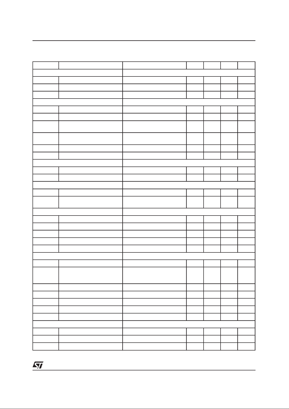
ABSOLUTEMAXIMUM RATINGS
Symbol Parameter Value Unit
V
CC
V
dd
V
in max
V
in min
SPINDLE I
VCM I
peak
P
(*) Maximum Total Power Dissipation ≈ 2.5
tot
T
stg,Tj
THERMAL DATA
Symbol Parameter Value Unit
R
th j-case
R
th j-amb
Maximum Supply voltage -0.5 to 14 V
Maximum Logic supply -0.5 to 6 V
Maximum digital input voltage Vdd+0.3V V
Minimum digital input voltage GND - 0.3V V
Spindle peak sink/source output current 2.1 A
peak
VCM peak sink/source output current 1.6 A
3 with soldered slug
≈
Maximum Storage/Junction Temperature -40 to 150 °C
Thermal Resistance Junction to Case
(*) Thermal Resistance to Junction to ambient
25 with soldered slug
≈
11 °C/W
≈
32
≈
W
W
°C/W
°C/W
(*) In typical application with multilayer 120mmx120mm Printead Circuit Board.
RECOMMENDED OPERATINGCONDITIONS
Symbol Parameter Value Unit
V
CC
V
dd
T
amb
T
j
ELECTRICAL CHARACTERISTICS
Supply voltage 10.8 to 13.2 V
Maximum Logic supply 4.5 to 5.5 V
Operating Ambient Temperature 0 to 70 °C
Junction Temperature 0 to 125 °C
(All specificationsare for 0 < T
<70°C, VCC= 12V; VDD= 5V,
amb
FLL_RES= 62kΩ, unless otherwisespecified.)
Symbol Parameter Test Condition Min. Typ. Max. Unit
POWER SUPPLIES
V
I
VCC
V
rectified
V
I
CC
dd
Vdd
12V Supply 10.8 13.2 V
VCCCurrent SPINDLE + VCM 20 mA
SPINDLE ONLY 7 mA
VCM ONLY 12 mA
VCCSupply Rectified 3.5 13.2 V
5V supply 4.5 5.5 V
5V supply SPINDLE + VCM 6 mA
SPINDLE ONLY 7 mA
VCM ONLY 12 mA
4/17
ELECTRICALCHARACTERISTICS (Continued)
Symbol Parameter Test Condition Min. Typ. Max. Unit
THERMAL SENSING
T
SD
T
HYS
T
EW
SUPPLY MONITOR
V
TR
V
HYS
I
DLY
R
on_por
V
DLY
I
IN
VOLTAGE BOOST
V
BOOST
F
osc
SW1 OUTPUT
R
GATE
V
GATE
DIGITAL LOGIC LEVELS
V
IH
V
IL
V
OH
V
OL
F
SYSCLK
VCM, DAC
T
C
VCM, ERROR AMPLIFIER
A
VOL
V
OS
I
IB
Shutdown Temperature 150 180 °C
Hysteresis 60 °C
Early Warning TSD-25 °C
Trip Point Input Rising 1.92 2 2.08 V
Hysteresis Voltage Input falling 100 mV
Porb Delay Current TR_5V, TR_12V> V
TR
1.5 2 2.5 µA
Vpordly = 2V
Porb Pull Down Ron Vdd> 2V and sink 1mA
V
=2V
pordly
Porb Dly Threshold TR_5V, TR_12V> V
TR
2.5 3.0 3.5 V
500
Input Current VIN<4V -1 1
Output Voltage VCC+5 VCC+6.3 V
Internal Oscillator 130 200 250 kHz
Gate Driver for External Mosfet Internal Resistor to CP 200 kΩ
Off Gate State Voltage for
IO= 1mA VCC= 3.5V 0.7 V
External Mosfet
Input Logic ”1” VDD= 5.5V 2.4 V
Input Logic ”0” VDD= 4.5V 0.5 V
Output Logic ”1” I
Output Logic ”0” I
=20µAV
SOURCE
= -400µA 0.4 V
SOURCE
-0.2 V
dd
System Clock 20 25 MHz
Resolution 14 Bits
Differential Linearity 1 LSB Change
-Tested
By design
-1
-0.5
1
0.5
Integral Linearity 9 Bits
Midscale Offset Referenced to V
/2 -5 5 mV
CC
Convertion Time 5
Full Scale Voltage Referenced to VCC/2
1V
±
Full Scale Error -4 4 %
Open Loop Gain DC 50 db
Input Offset Voltage -5 5 mV
Input Bias Current -250 250 nA
L6268
Ω
A
µ
LSB
s
µ
5/17
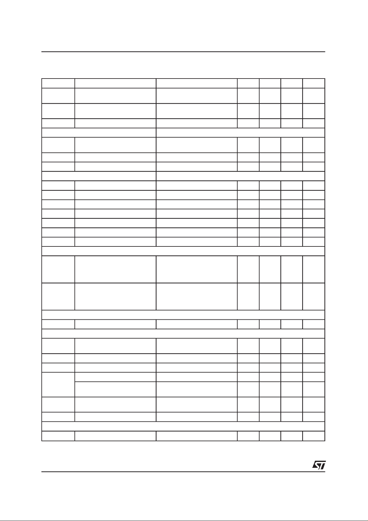
L6268
ELECTRICALCHARACTERISTICS (Continued)
Symbol Parameter Test Condition Min. Typ. Max. Unit
V
ICM
Vclamp Output Clamp Voltage -1mA < I
F
ODB
VCM, POWER STAGE
R
DS(ON)
I
O
I
O(LEAK)
VCM, CURRENT SENSE ANPLIFIER
A
V
V
ICM
V
OCM
V
OS
F
3dB
CMRR Input Common Mode Rejection 50 dB
PSRR Power Supply Rejection Ratio 60 dB
VCM, RETRACT
Vpark RETRACT VOLTAGE PKV_1 = 0 & PKV_2 = 0
Tretract Retract Time
SPINDLE, PWM CURRENT SENSE COMPARATOR
T
DLY
SPINDLE, POWER STAGE
R
DS(ON)
I
O
I
O(LEAK)
dV
O/dt
BEMF
V
HYS
FLL CHARGE PUMP OUTPUT
I
LEAK
Input Common Mode Range VCC/2-
0.5
<1mA
O
Lowside/Highside clamp
VCC/2±
2.2V
VCC/2+
0.5
Unity Gain Bandwidth 10 MHz
Output ON Resistance (Each
device)
Tj=25°C
T
= 125°C
j
0.5
0.8
Operating Current 1.3 A
Output Leakage Current VCC= 14V 1.0 mA
Voltage Gain 3.88 4 4.12 V/V
Input Common Mode Range -0.3 VCC+0.3 V
Output Common Mode Range -3mA < IO<3mA 2 VCC-2 V
Output Offset Voltage SENSE_IN (±)=VCC/2 -15 15 mV
3dB Bandwidth 1 MHz
850
650
1600
1150
320
640
160
320
limited by the internal oscillator
200kHz
PKV_1 = 0 & PKV_2 = 1
PKV_1 = 1 & PKV_2 = 0
PKV_1 = 1 & PKV_2 = 1
RT0 = 0 & RT1 = 0
RT0 = 0 & RT1 = 1
RT0 = 1 & RT1 = 0
RT0 = 1 & RT1 = 1
Delay to FCOM Out 200 500 ns
Output On Resistance (Each
device)
Tj=25°C
T
= 125°C
j
0.45
0.74
Start-Up Current 2A
Output Leakage Current VCC = 14V 1.0 mA
Output Slew Rate (Linear) R
Output Slew Rate (PWM) Reg#8Eh, Bit 0 = 0
Minimum BENF Voltage for
MIN
= 100k
slew
Ω
Reg#8Eh, Bit 0 = 1
0.2 0.3 0.5 V/µs
10
20
20 28 40 mVp-p
Detection
Hysteresis 15 mV
Off State Leakage 0 < Vfll_res , 3V -50 +50 nA
V
V
Ω
Ω
mV
mV
mV
mV
ms
ms
ms
ms
Ω
Ω
V/µs
V/µs
6/17

ELECTRICALCHARACTERISTICS (Continued)
Symbol Parameter Test Condition Min. Typ. Max. Unit
I
O
V
RCP
CURRENT SENSE AMPLIFIER
I
BIAS
Av Voltage Gain 3.8 4.0 4.2 V/V
dV
o/dt
SERIAL PORT
Symbol Parameter Min. Typ. Max. Unit
T
SCK
T
CKL
T
CKH
T
SDENS
T
SDENH
T
DS
T
DH
T
SDENL
T
SDV
T
SDV
On State Current FLL_RES = 62k
ICP = ”1”
ICP = ”0”
Current Set Voltage FLL_RES = 62k
Ω
22
80
Ω
1.18 1.225 1.25 V
25
100
32
120
Input Bias Current 2
Output Slew Rate 20 V/µs
SCLK Period 40 ns
SCLK low time 15 ns
SCLK high time 15 ns
Enable to SCLK 35 ns
SCLK to disable 20 ns
Data set-up time before rising edge SCLK 10 ns
Data Hold Time 10 ns
Minimum SDEN Low Time 50 ns
SCLK falling edge (A6) to SDATA valid on READ op. 3 10 ns
SCLK rising edge (D0-D7) to SDATATransition onREAD op. 5 35 ns
L6268
µA
µA
A
µ
Figure 1. SerialPort Timing Information.
SDEN
SCLK
SDATA
SDEN
SCLK
SDATA
0A0A1
1st Byte 2nd Byte
1A0A1
1st Byte 2nd Byte
A6 D0 D1 D2 D7
SERIAL PORT WRITE TIMING
A6 D0 D1 D2 D7
SERIAL PORT READ TIMING
D98IN844
7/17

L6268
SERIAL PORTOPERATION
The serial port interface is a bi-directional port for reading and writing programming data from/to the internal registers of this device. For data transfers SDEN* is brought high, serial data is presented at the
SDATA pin, and a serial clock is applied to the SCLK pin. After the SDEN* goes high , the first 16 pulses
applied to the SCLK pin will shift the data presented at the SDATA pin into an internal shift register on
the rising edge of each clock. An internal counter prevents more than 16 bits from being shifted into the
register. The data in the shift register is latched after the 16th SCLK pulse. If less than 16 clock pulses
are provided before SDEN* goes low, the data transferis aborted.
All transfers are shifted into the serial port LSB first. The first byteof the transfer is for R/W and address
and instructioninformation.The first bit is R/W instruction bit, 0 is for WRITE and 1 is for READ.
Following7 bits are Address.
Figure 2. SerialPort Data Transfer Format.
SDEN
SDATA
INSTRUCTION, 1 BIT
ADDRESS, 7 BITS
DATA, 8 BITS
SCLK
D98IN845
INTERNALREGISTER DEFINITION
Reg:
Name:
Type:
Address:
BIT LABEL DESCRIPTION
0 VDAC BIT8 VCM DAC bit 8
1 VDAC BIT9 VCM DAC bit 9
2 VDAC BIT10 VCM DAC bit 10
3 VDAC BIT11 VCM DAC bit 11
4 VDAC BIT12 VCM DAC bit 12
5 VDAC BIT13 MSB resistor ladder of the 14 bit VCM DAC
6 PSM/LINEAR Selects Voice Coil PSM or Linear Output Current Control. 1=PSM
7 VCM_CAL VCM calibration. 1 = Enables VCM control circuits and tristates
0
VCM DAC (High) Register
Write only
0Eh
0=Linear.
VCM power transistors.
8/17
L6268
INTERNALREGISTER DEFINITION
VCM DAC (High and Low)Registers
Bit 0 through 5 of the VCM DAC (High) Registers and bit 0 through 7 of the VCM DAC (Low) Registers
control the absolutevalue of the voice coil current. Bit is the sign bit, controlling the current direction. All
the 13 bitsare part of a resistordivider network.
Note. It is required to write on register 1 to make effectivechanges on register 0.
Reg:
Name:
Type:
Address:
BIT LABEL DESCRIPTION
0 VDAC BIT0 LSB resistor ladder of the 14 bit VCM DAC
1 VDAC BIT1 VCM DAC bit 1
2 VDAC BIT2 VCM DAC bit2
3 VDAC BIT3 VCM DAC bit3
4 VDAC BIT4 VCM DAC bit4
5 VDAC BIT5 VCM DAC bit5
6 VDAC BIT6 VCM DAC bit6
7 VDAC BIT7 VCM DAC bit7
Reg:
Name:
Type:
Address:
1
VCM DAC (Low) Registers
Write only
1Eh
2
Spindle Control Register
Write only
2Eh
BIT LABEL DESCRIPTION
0 INCRE_SEQ A 0 to 1 transition of this bit increments the spindle Sequencer.
1 START_UP 1 = Spindle Internal start up, 0 = Spindle External start up
2 R_SEQ Reset Spindle sequencer. 1 = Reset sequencer to phase 1.
3 RUN 1 = Start Spindle ALIGN & GO, 0= Reset Spindle control logic.
4 SPIN_EN Enable Spindle section. 1 = Enable, 0 = Disable.
5 MEC/ELEC Specifies electrical or mechanical cycle for Spindle FLL control.
6 PWM/LINEAR Selects Spindle PWM or Linear Output Current Control. 1 = PWM,
7 EXT/INT External or internal Spindle loop feedback. 1 = external feedback
1=Electrical, 0 = Mechanical.
0=Linear.
via index pin.
9/17

L6268
INTERNALREGISTER DEFINITION
Reg:
Name:
Type:
Address:
BIT LABEL DESCRIPTION
0 MASK_TIME Spindle BEMF Mask Time. 0 = 15 degree, 1 = 7.5 degree
1 MIN2 Control Spindle PWM on time Min 1 Min2 Min. on Time
2 MIN1 0 1 1.4µs
3 8_12_POLE Selects 8 or 12 pole motors. 1 = 8 pole, 0 = 12 pole.
4 SD3 Spindle commutation delay MSB
5 SD2 Spindle commutation delay bit
6 SD1 Spindle commutation delay bit
7 SD0 Spindle commutation delay LSB
3
Spindle Delay Register
Write only
3Eh
0 0 5.9µs
10 12
s
µ
SPINDLEPHASE DELAY
SD3-0 set the phase delay from BEMF zero crossing to the next commutation.The 30 theoreticaldegree
value can be changedto compensate for switchingand other delays that are always present.The delay
adjustmentrange is from1.875 throughto 30 electricaldegreesin 1.875 degree increments.
Reg:
Name:
Type:
Address:
BIT LABEL DESCRIPTION
0 C4 Bit 4 of Spindle FLL Coarse Counter
1 C5 Bit 5 of Spindle FLL Coarse Counter
2 C6 Bit 6 of Spindle FLL Coarse Counter
3 C7 Bit 7 of Spindle FLL Coarse Counter
4 C8 Bit 8 of Spindle FLL Coarse Counter
5 C9 Bit 9 of Spindle FLL Coarse Counter
6 C10 Bit 10 of Spindle FLL Coarse Counter
7 C11 MSB of Spindle FLL Coarse Counter
10/17
4
FLL Coarse Counter Register
Write only
4Eh

INTERNALREGISTER DEFINITION
L6268
Reg:
Name:
Type:
Address:
BIT LABEL DESCRIPTION
0 F8 Bit 8 of Spindle FLL Fine Counter
1 F9 Bit 9 of Spindle FLL Fine Counter
2 F10 MSB of Spindle FLL Fine Counter
3 Unused. Set = 0
4 C0 LSB of Spindle FLL Coarse Counter
5 C1 Bit 1 of Spindle FLL Coarse Counter
6 C2 Bit 2 of Spindle FLL Coarse Counter
7 C3 Bit 3 of Spindle FLL Coarse Counter
Reg:
Name:
Type:
Address:
5
FLL Coarse/FineCounter Register
Write only
5Eh
6
FLL Fine Counter Register
Write only
6Eh
BIT LABEL DESCRIPTION
0 F0 LSB of Spindle FLL Fine Counter
1 F1 Bit 1 of Spindle FLL Fine Counter
2 F2 Bit 2 of Spindle FLL Fine Counter
3 F3 Bit 3 of Spindle FLL Fine Counter
4 F4 Bit 4 of Spindle FLL Fine Counter
5 F5 Bit 5 of Spindle FLL Fine Counter
6 F6 Bit 6 of Spindle FLL Fine Counter
7 F7 Bit 7 of Spindle FLL Fine Counter
11/17

L6268
INTERNALREGISTER DEFINITION
Reg:
Name:
Type:
Address:
BIT LABEL DESCRIPTION
0 THERMAL Thermal Shutdown = 0 indicates that the chip temperature has exceeded 160°C.
1 THERM_WARN Thermal Shutdown Warning =0 indicates that the chip temperature is
2 ROTOR_STUCK 0 = A sequentialSpindle BEMF has not been detected
3 FAULT 1 = Rapid deceleration of the Spindle motor or High frequency on FCOM signal.
4 MASK_TIME Mask Time toggled to ”0” indicates thatthe Spindle BEMF is masked.
5 ERROR_LOCK 0 = Indicates error Spindle speed > 16msec/sample, either electrical or
6 ALIGN 0 indicate that the Spindle is in the Internal Start-Up Align Phase.
7 GO 0 indicate that the Spindle is in the Internal Start-Up Go Phase.
Reg:
Name:
Type:
Address:
7
Spindle StatusRegister
Read only
7Eh
The bit will reset (=1) when the temperature falls below 130°C. When Thermal
Shutdown =0, the spindle logic will tristate both high and low side drivers,
protecting the output circuitry.
approximately 25°C before the device goes inthermal shut down.
mechanical.
8
Spindle FLL Register
Write only
8Eh
BIT LABEL DESCRIPTION
0 SSLEW Spindle PWM (chopping) Slew Rate. 0 = 10VµS, 1 = 20VµS
1 ICP Spindle FLL Charge pump current. 1= 25µA, 0 = 100µA.
2 Unused. Set= 0.
3 ISNS 1 = Puts outputof the Spindle sense amplifier on FCOM pin and changes limit to
4 IL1 Adjust maximum voltage on SpindleRsense
5 IL0 Adjust maximum voltage on SpindleRsense
6 CPL 1 = Spindle FLL Charge pump low
7 CPH 1 = Spindle FLL Charge pump high
”IL0” ”IL1” ”ISNS” V(I_SENSE) LIMIT (±10%)
0 0 0 0.45V
1 0 0 0.50V
0 1 0 0.55V
1 1 0 0.75V
0 0 1 0.15V
1 0 1 0.20V
0 1 1 0.25V
1 1 1 0.30V
12/17
roughly 1/3 of normal.

INTERNALREGISTER DEFINITION
L6268
Reg:
Name:
Type:
Address:
BIT LABEL DESCRIPTION
0 PKV_1 VCM Parking Voltage
1 PKV_2 VCM Parking Voltage
2 VR 1 = connects internal VR reference (2V) to level shift Opamp (for
3 RT0 (*) VCM Retract Time
4 DOUBLE 1 = Spindle Internal Start-UpAlign and Energizationtime doubled.
5 VCM_EN Enable VCM section. 1 = Enable, 0 = Disable.
6 RT1 (*) VCM Retract Time
7 RETRACT 1= VCM retract
(*) When program Retract Time (RT0 and RT1), Bit 2 REG#8Eh mustbe always written to0.
9
SystemControl Register
Write only
9Eh
Vcm calibration).
”PKV_1” ”PKV_2” ”PARKING VOLTAGE”
0 0 0.850V
0 1 0.650V
1 0 1.600V
1 1 1.150V
”RT0” ”RT1” ”RETRACT TIME”
0 0 320ms
0 1 640ms
1 0 160ms
1 1 320ms
13/17

L6268
INTERNALREGISTER DEFINITION
Reg:
Name:
Type:
Address:
BIT LABEL DESCRIPTION
0 Unused. Set = 0
1 Unused. Set = 0
2 Unused. Set = 0
3 Unused. Set = 0
4 FLL_OUT 1 = Spindle Mech/Elec(see bit 5 register 2) output, 0 = Spindle
5 REV_BRAKE Spindle Reverse Brake command. 1 = Brake. “0” has to be
6 Unused. Set = 0
7 VB/DIS 1 = Disable Vboost
Reg:
Name:
Type:
Address:
10
Test ControlRegister
Write only
AEh
zero crossing output.
reinserted to enable the spindle start up.
11
VCM Control Register
Write only
BEh
BIT LABEL DESCRIPTION
0 VCMS VCM PSM (chopping) Slew Rate. 0 = 10V/µs, 1 = 20V/µs
1 VCMH 1 = Forces VCM outputsto be High in PSM mode.
2 SLEEP Unused (for futurepower saving mode).
3 COMSLEW Spindle PWM (phase commutation) Slew Rate. 0 = 30Vµs, 1 =
4 Unused. Set = 0
5 Unused. Set = 0
6 Unused. Set = 0
7 Unused. Set = 0
14/17
2Vµs.

INTERNALREGISTER DEFINITION
L6268
Reg:
Name:
Type:
Address:
12
Chip ID Register
Read only
FFh
BIT LABEL DESCRIPTION
0 ID_REV_0 Minor Revision Bit 0.
1 ID_REV_1 Minor Revision Bit 1.
2 ID_REV_2 Minor Revision Bit 2.
3 ID_REV_3 Minor Revision Bit 3.
4 ID_REV_4 Minor Revision Bit 0.
5 ID_REV_5 Minor Revision Bit 1.
6 ID_REV_6 Minor Revision Bit 2.
7 ID_REV_7 Minor Revision Bit 3.
Figure 3. ApplicationCircuit.
100nF
2.2µF
220pF(3)
5K(4)
15K
22µF
16V
(1)
1N4148
51K
10nF(4)
1µF
VCC
1N4148
100nF
22µF
16V
(1)
47nF
SW1
POR_DELAY
BRK_CAP
PWM/SLEW
DGND
SPN_COMP
AGND
TR_12V
GND
VDD
TR_5V
Voice Coil Ground
Power Ground
0.3(1W)
100nF
VCC RSENSE ISENSE2CTAP
CS
24
CP
23
33
36
12
3
14
44
42
40
8
19
35
VCM_CAL22V12/2 DAC ERROR_IN ERROR_OUT SENSE_OUT
13,43 6,9 5
20 41 39 38 37
10K 62K 10K
Analog Ground (1) This capacitormust be
Digital Ground
CTAP
OUT_A
1nF
(2) Place these components close to
(3) Do not mount this component if Spindle Linear mode is
(4) Do not mount this component if Spindle Pwm mode is used
OUT_A
OUT_B
10
Tantalum
12V_VCC
12V_VCC
5V_VDD
STN4NE03
5K(4)
20K
18.2K
OUT_B
7
thedevice
OUT_C
OUT_C
4
28
VCM_GND
25,31
26
27
30
29
21
32
11
1
34
15
18
17
16
VCM_A-
SENSE_IN+
VCM_A+
SENSE_INFLL-FILTER
FLL_RES
VCC
INDEX
FCOM
PORB
SYS_CLK
SCLK
SDATA
SDEN
used
VCM_A-
0.25(1W)
62K
4.7K
D99IN1049
1µF
VCM_A+
620K
100nF
VCC
INDEX
FCOM
5V_VDD
PORB
SYS_CLK
SCLK
SDATA
SDEN
15/17
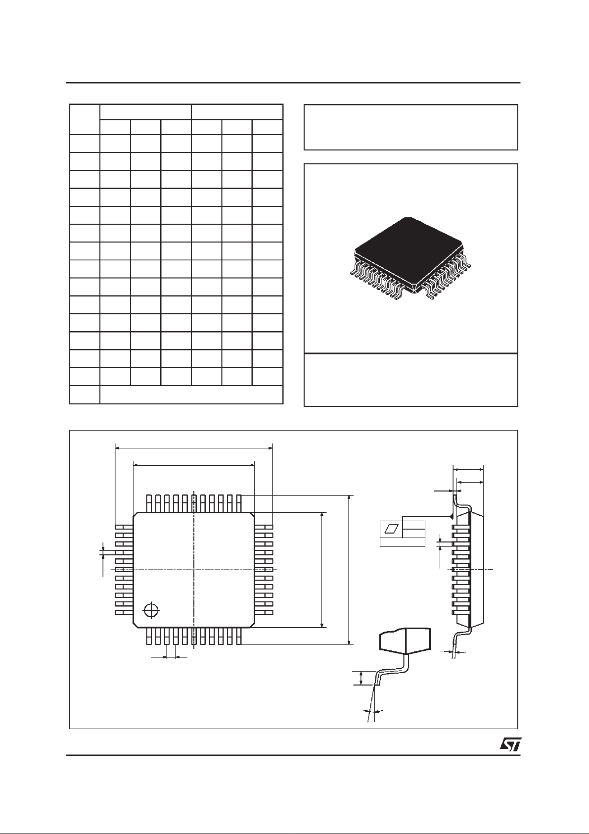
L6268
DIM.
mm inch
MIN. TYP. MAX. MIN. TYP. MAX.
A 1.60 0.063
A1 0.05 0.15 0.002
0.006
A2 1.35 1.40 1.45 0.053 0.055 0.057
B 0.30 0.37 0.45 0.012 0.014 0.018
C 0.09 0.20 0.004
0.008
D 12.00 0.472
D1 10.00 0.394
D3 8.00 0.315
e 0.80 0.031
E 12.00 0.472
E1 10.00 0.394
E3 8.00 0.315
L 0.45 0.60 0.75 0.018 0.024 0.030
L1 1.00 0.039
K 0°(min.), 3.5°(typ.),7°(max.)
OUTLINE AND
MECHANICAL DATA
TQFP44 (10 x 10)
D
D1
A1
2333
34
B
44
1
e
11
TQFP4410
22
E
E1
12
L
0.10mm
.004
Seating Plane
B
K
A
A2
C
16/17

L6268
Information furnished is believed to be accurate and reliable. However, STMicroelectronics assumes no responsibility for the consequences
of use of such information nor for any infringement of patents or other rights of third parties which may result from its use. No license is
granted by implication or otherwise under any patent or patent rights of STMicroelectronics. Specification mentioned in this publication are
subject to change without notice. This publication supersedes and replaces all information previously supplied. STMicroelectronics products
are not authorized for use as critical components in life support devices or systems without express written approval of STMicroelectronics.
The ST logois a registeredtrademark of STMicroelectronics
1999 STMicroelectronics – Printed in Italy – All Rights Reserved
STMicroelectronics GROUP OF COMPANIES
Australia - Brazil - Canada - China - France - Germany - Italy- Japan - Korea - Malaysia - Malta - Mexico - Morocco - The Netherlands-
Singapore- Spain - Sweden - Switzerland - Taiwan - Thailand - United Kingdom- U.S.A.
http://www.st.com
17/17
 Loading...