

L6260
4.5 – 5.5V DISK DRIVER SPINDLE & VCM,
POWER & CONTROL COMBO’S
GENERAL
5V OPERATION. *REGISTERBASED ARCHITECTURE
MINIMUMEXTERNALCOMPONENTS
SLEEP AND IDLE MODES FOR LOW
POWERCONSUMPTION
SELECTABLE GAINS FOR BOTH V.C.M.
AND SPINDLE
10 BIT (+ SIGN + GAIN ) VCM & 8 BIT SPIN-
DLE DACs
HIGH BANDWIDTH SPEED REGULATION
LOOP (ONCE PER MECH\ELEC CYCLE ACCURACY)
VCM DRIVER
CURRENT SENSE CONTROL (VOLTAGE
PROPORTIONALTO CURRENT)
300mADRIVE CAPABILITY
TWO CURRENT RANGES FOR SEEKING
AND TRACKING
INTERNAL REGISTER FOR POWER AMP
CONTROLLINES
SPINDLEDRIVER
BEMF PROCESSING FOR SENSORLESS
MOTOR COMMUTATION
PROGRAMMABLE COMMUTATION PHASE
DELAY
PROGRAMMABLE SLEW-RATE FOR REDUCED E.M.I.
0.8Ω FOR ANYHALF BRIDGE WORST CASE
SYNCHRONOUS RECTIFICATION OF THE
B.E.M.F.DURING RETRACT OPERATION
BIPOLAR\ TRIPOLAR OPERATION
SYNTHESIZEDHALL OUTPUTS
1.0 AMPDRIVE CAPABILITY
OTHER FUNCTIONS
POWERUP SEQUENCING
POWERDOWN SEQUENCING
LOW VOLTAGE SENSE
ACTUATORRETRACTION
DYNAMICBRAKE
THERMALSHUTDOWN
BICMOS TECHNOLOGY
TQFP64
ORDERING NUMBER: L6260
THERMAL& CURRENT PROTECTION
DESCRIPTION
The L6260 is single chip sensorless (DC) spindle
motor and voice coil controllers including power
stages suitablefor usein smalldisk drives.
These devices have a serial interfacefor a microprocessorrunning up to 10 Mega bits per second.
There are registers on chip to allow the setting of
the desired spindle speed via the on chip FrequencyLocked Loop (F.L.L.). No externalcomponents are requiredin the sensor-lessoperation as
the control functions are integrated on chip (e.g.
B.E.M.F.processing, digital masking, digitaldelay
and sequencing).
The V.C.M. driversuses a transconductanceamplifier, able to provide 2 different current ranges,
suitable forseeking and tracking.
When a low voltage is detected,a Power On Reset (P.O.R.) is issued and the internal registers
are reset, the spindle power circuitry is tri-stated,
B.E.M.F.synchronous rectification is enabled, the
actuator retracts and then dynamic braking of the
spindle is applied.
These devices are built in BICMOStechnologyallowing dense digital circuitry to be combined with
MOS\Bipolarpower devices.
November 1996
1/30
L6260
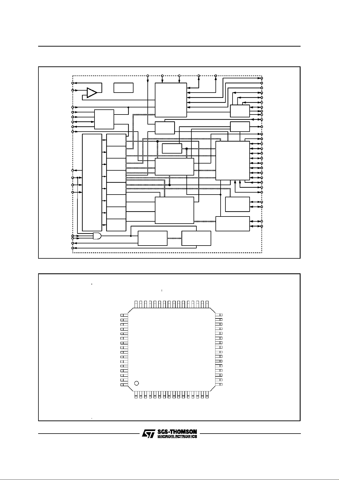
BLOCK DIAGRAM
VREFOUT
VREF/MINUS
DAC/GND
UV1
UV2
POR/DLY
POR
FCLK
SDIO
SCLK
SLOAD
R/W
TEST
TRISTATE
ATEST
DTEST
177
+
SERIAL
PORT
INTERFACE
POWER
MONITOR
CIRCUIT
REGISTER
0
REGISTER
1
REGISTER
2
REGISTER
3
REGISTER
4
REGISTER
5
REGISTER
6
REGISTER
7
BIAS
PARK/V VCM/COMP
VCM LOGIC &
VCM
PARK
ANALOG TEST
CIRCUIT
DAC
BEMF
AMP
SPINDLE
LOGIC
SPINDLE
FLL
DIGITAL TEST
CIRCUIT
VCM/PLUSVCM/I/SNS/2VCM/I/SNS/1
VOLTAGE
TRIPLER
CENTER TAP
DRIVER
SPINDLE
BLOCK
& DAC
CURRENT
GENERATOR
CHARGE
PUMP
VCM/MINUS
VVCM/2
VVCM/1
C1LOW
C1HIGH
C2LOW
C2HIGH
VHTRIP
VLTRIP
VPARKOUT
CTAP
SYNTH/HALL
VRECT
VSPIN/1
VSPIN/2
SPN/I/SNS
COIL/A
COIL/B
COIL/C
SPIN/GND1
SPIN/GND2
VPDOWN
BRK/DLY
SPN/I/COMP
SPN/SLEW
FLL/RES
SPD/COMP
SPD/COMP/SHT
D94IN087
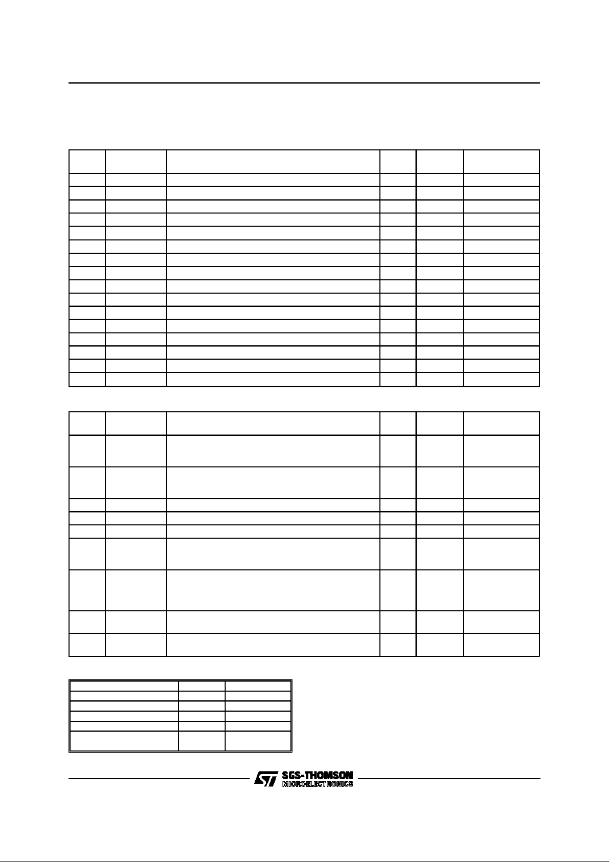
PIN CONNECTION(Top view)
SPN_DSBL_DLY
POR_DLY
VCM_I_SNS1
VVCM_1
VCM_MINUS
VCM_I_SNS2
VCM_PLUS
VVCM_2
C1HIGH
C1LOW
TRIPGND
C2HIGH
2/30
GND
UV
CTAP
ATEST
GND
GND
PARKV
AGRND
DACGND
VFER_MINUS
REF OUT
VCC
SPIN SLEW
FLL RES
SPD COMP SHT
48
49
64
116
L
ND
OW
G
2
C
RIP
T
L
V
OR
RIP
P
HT
V
P
COM
M
C
V
GND
IG
D
C
D
V
D
A
O
L
S
K
DIO
CL
S
S
SPD COMP
K
L
C
F
T
C
E
R
V
GND
S
NS
ND
I
G
N
P
S
33
GND
32
17
GND
VSPIN_2
VPDOWN
COIL_C
BRK_DLY
SPIN_GND_2
EXTFLL/DTEST
COIL_B
TRISTATE
VSPIN_1
SYNTH_HA LL
TEST
COIL_A
R/W_
SPN_GND_1
GND
GND
VPARKOUT
SPN1 COMP
PIN DESCRIPTION
Pin Types:I = Input,O = Output,P = Power, A= Analog (passive)
Power
L6260
PIN # PIN NAME DESCRIPTION
8 VDC Digital power. Positivenominally 5V or 3V AI No No
41 VCC Analog power. Positivenominally 5Vor 3V AI No No
54 VVCM_1 VCM power supply. Positive nominally 5V or 3V AI No No
58 VVCM_2 Same as above AI No No
23 VSPIN_1 Spindle power pin.Positive nominally 5V or 3V AI No No
31 VSPIN_2 Same as above AI No No
1 GND Ground AI No No
15-17 GND Ground AI No No
32-34 GND Ground AI No No
47-49 GND Ground AI No No
18 SPN_GND_1 Ground forspindle circuit AI No No
27 SPN_GND_2 As above AI No No
44 DAC_GND Ground forall DACs AI No No
45 AGND Analog ground AI No No
7 DIG_GND Digital ground AI No No
63 TRIPGND Voltage triplerground AI No No
PIN
TYPE
I\O
MAPPED?
TRI-STATE
@SLEEP/@POR
Serial Interface& Test Pins
PIN # PIN NAME DESCRIPTION
12 FCLCK System clock. 4-12MHz selectable via the
CLK_PRESCALE bit inthe System Control Register
B (Reg 4 Bit 4).
11 SDIO Serial port data I/O running up to 10MHz. For full
details of allserial port signals see theCircuit
Description section.
10 SCLK Serial port clock (max 10Mbits/s) DI Yes No
19 R/W Read / Write signal for serial interface DI Yes No
9 SLOAD Chip select input. DI Yes No
21 TEST Used to enable one of the test modes. The mode is
selcted in conjunction with the TRISTATE pin (see
below for more details).
24 TRISTATE Used to enable one of the test modes. The mode is
selcted in conjunction with the TEST pin (see below
for more details).This pin has no effect on the
spindle or VCM drivers, this is a test pin only.
60 ATEST Analog test pin. This pin carries the required analog
signal to allow external testing.
26 DTEST Digital Test Output Pin. This pin also doubles as the
Clock input if an external FLL is used.
PIN
TYPE
DI Yes No
DI/O Yes Yes
DI No No
DI No No
AO No No
DI/O No No
I\O
MAPPED?
TRI-STATE
@SLEEP/@POR
Test Mode TEST pin TRISTATE pin
IOMAPPING Test 1 0
DIGITAL Test* 1 1
ANALOG Test* 1 1
TRISTATE Test 0 1
Normal Operation (non
test mode)
00
For a detailed description please refer to the Test
Circuit section of the CIRCUIT OPERATION portion ofthis datasheet
* These two test modes operatesimultaneously through separate
test pins (ATESTand DTEST).
3/30
L6260
PIN DESCRIPTION(continued)
Pin Types:I = Input,O = Output,P = Power, A= Analog (passive)
VCM Driverand DAC
PIN # PIN NAME DESCRIPTION
53 VCM_I_SNS1 High side ofVCM sense resistornetwork. This pin
provides the current to the network as well as
sensing the total voltage across both sense
resistors. Sensing the total drop across both
resistors results in the low transconductancegain
feedback used fortrack following.
56 VCM_I_SNS2 Sensing across the lower VCM sense resistor for
high transconductance gain feedback for seek
operations.
6 VCM_COMP VCM compensation network. Typically, 200KΩin
series with 100nF is connected from this pin to
Ground.
57 VCM_PLUS VCM Power Amplifierpositive output terminal A No No
55 VCM_MINUS VCM Power Amplifier negativeoutput terminal A No No
46 PARK_V A resistor conneced between this pin and
VCM_PLUS determines the Parking Voltage
35 VPARKOUT Output from the retract circuit. This pinis usually
directly connected to the VCM_MINUS.
PIN
TYPE
ANo No
ANo No
ANo No
ANo No
AO No No
Spindle Driver and DAC
PIN # PIN NAME DESCRIPTION
40 SPN_SLEW The External.SpindleDriver Slew Rate resistor
(Rslew), typically250K isconnected from thispin to
Ground. When in nExternal Slew Rate Mode
(System Control Register B, Bit 10=0), the slew rate
is determined by:
SlewRate = (0.5Vto Rslew) X (DACslew+1) +20pF
DAC slew = System Control Register bits 7 - 9.
36 SPN_I_COMP A seroies RC network from this pin to ground sets
the spin drivercompensation. Typical a single 4nF
capacitor will provide adequate compensation.
14 SPN_I_SNS A current sensing resistor (2.5KΩTypical ).is
connected from this pin to ground. See the Circuit
Operation section for details.
20 COIL_A Spindle Power Amplifieroutput A. Also serves as
BEMF sensing forPhase A.
25 COIL_B Spindle Power Amplifieroutput B. Also serves as
BEMF sensing forPhase B.
29 COIL_C Spindle Power Amplifier output C. Also serves as
BEMF sensing forPhase C.
59 CTAP Spindle Motor Center Tap connection A No No
22 SYNTH_HALL CMOS level spindle speed output.When SYNHALL
(System Control Register B, bit 5) is set to 0, this
output switches stateat every zerocrossing of any
phase. With SYNHALL = 1, the output only switches
every zero crossingof Phase A.
37 SPD_COMP Change Pump RC network connection pin for FLL
mode operation.
38 SPD_COMP_SHTThis pin allows for shorting ofto the Charge Pump
Network resistor. This operation provides a quick
charge on the Charge Pump capacitor, reducing
settling time oncedesired speed isreached.
Operation is controlledby bit 9 of System Control
Register A.
39 FLL_RES Frequency LockedLoop charge pump gain resistor.
(Rep), typically 12.5KΩ , is connectedfrom this pin
to Ground. Change Pump current is determined by:
I = (0.5Vto Rcp) X (FLLGAIN DAC +1)
FLLGAIN DAC = System Control Register B bits 0-4
PIN
TYPE
ANo No
ANo No
AO No No
ANo No
ANo No
ANo No
DO Yes Yes
ANo No
ANo No
ANo No
I\O
MAPPED?
I\O
MAPPED?
@SLEEP/@POR
@SLEEP/@POR
TRI-STATE
TRI-STATE
4/30
PIN DESCRIPTION(continued)
Pin Types:I = Input,O = Output,P = Power, A= Analog (passive)
Power down sequencing, POR, other voltage pins
L6260
PIN # PIN NAME DESCRIPTION
13 VRECT Outputofthe synchronous rectifiersupplying powerto
28 BRK_DLY An external parallel RC network from thispoint to
30 VPDOWN Voltage triplerreservoir capacitor. Thisis used for
61 C1HIGH Positive terminalof charge pump capacitor.
62 C1LOW Negative terminal of charge pump capacitor.
64 C2HIGH Positive terminalof charge pump capacitor for
2 C2LOW Negative terminal of charge pump capacitor for
52 POR_DLY An external capacitor from this pinto ground sets
5 POR Power On Reset. Thisopen drain output goeslow
50 UV1 Under voltage detector 1.This defines the
51 SPN_DSBL_
DLY
4 VHTRIP High tripler/Doubler output. 330nF (typ). 11V max. AO No No
3 VLTRIP Low tripler/Doubler output. 330nF (typ). for stability. AO No No
theretractcircuitry.Filteredbyan internal 400pF
capacitor.Normally notexternallyconnected.However,
ifretractcommandistobeused, asmall signalsilicon
diodemustbeconnectedbetweenthispinandVcc
(Cathode to VRECT)to supply theadditional current
whichmaybe requiredtobrakethe VCM.
ground sets the Brake dELAY:T= 0.45 RC.
Typical values are R = 4MΩ, C=0.1µF (0.16sec,
delay).
the brake operation when power is removed from
the chip. NoDC load allowed.1µF minimum, 10µF
prefered.
10nF (typ) for Tripler operation;
330nF (typ0 or Doubler operation
10nF (typ) for Tripler operation;
330nF (typ)or Doubler operation
Tripler operation. 330nF (typ).
Connected tp VHRTRIP for Doubler operation.
Tripler operation. 330nF (typ).
Not connected forDoubler operation.
the duration of POR after power has been re-
established. T (por)= 32 X C (por)
where: C (por)is in pFand T is expresssed in µs.
when the voltageat either UV1 or UV2 goesbelow
1.25V.
VOLTAGE GOOD thresholdby comparing the
voltage on this pin to the internal 1.25V reference.
An external resistor divider network and capacitor
filter provides the selection of threshold and supply
noise rejection. There is an internal pull-up (2µA
max). Hysteresis is 20mV.
Spindle Disable Delay. A capacitor connected
between this pin and Vcc programs the delay
between POR and the disabling of the Spindle
section..
Delay = 80 xC (C in pF; Delay in µs)
PIN
TYPE
AO No No
ANo No
ANo No
ANo No
ANo No
ANo No
ANo No
ANo No
DO Yes No
AI Yes No
AI Yes No
I\O
MAPPED?
TRI-STATE
@SLEEP/@POR
5/30
L6260
PIN DESCRIPTION(continued)
Pin Types:I = Input,O = Output,P = Power, A= Analog (passive)
AuxiliaryFunctions
PIN # PIN NAME DESCRIPTION
PIN
TYPE
I\O
MAPPED?
TRI-STATE
@SLEEP/@POR
42 REFOUT Output from auxiliaryOPAMP. A No No
43* VREF_MINUS
(L6260 only)
26 EXTFLL/
DTEST
Negative input toauxiliary OPAMP. This is prsent
ONLY on the L6260.
See previous description of this pin(Serial interfaca
& Test Pinsection).
ANo No
DI/O No No
ABSOLUTE MAXIMUM RATINGS
Symbol Parameter Value Units
V
dd,Vp max
V
in max
V
in min
I
peak
I
dc
P
tot
T
stg,Tj
Maximum Supply voltage 6.5 V
Maximum input voltage Vdd + 0.3V V
Minimum input voltage GND - 0.5 V V
Peak sink/source output current 1.5 A
DC sink source output current 1.0 A
Maximum Total Power Dissipation 1.0 W
Maximum storage/junction temperature -40 to 150 °C
POWERDISSIPATION
Symbol Parameter Test Condition Min. Typ. Max. Units
V
dd,Vp
READY QUIESCENT CURRENT VCM ENABLED SPINDLE
IDLE QUIESCENT CURRENT VCM DISABLEDSPINDLE
SLEEP QUIESCENT CURRENT VCM DISABLEDSPINDLE
Supply voltage range 4.5 5.5 V
20 mA
ENABLED
10 mA
ENABLED
5mA
DISABLED
THERMAL DATA
Symbol Parameter Value Unit
R
th j-case
R
th j-amb
(*) In typical application with multiplayer printed circuit board.
Thermal Resistance Junction to Case 10
(*) Thermal Resistance Junction toCase 41.5
RECOMMENDED OPERATING CONDITIONS
Symbol Parameter Value Unit
Supply Voltage 4.5 to 5.5 V
Operating Ambient Temperature 0 to 70 °C
Junction Temperature 0 to 125 °C
6/30
V
ddn
T
amb
T
j
C/W
°
C/W
°
ELECTRICALCHARACTERISTICS
VCM Driver
Symbol Parameter Test Condition Min. Typ. Max. Units
I
ocr
I
ofr
ABEF Source & Sink On Resistance
R
dson
R
dson
V
jump
V
deadband
I
csbias
PSRR DC Power Supply Rejection
BW Current LoopBandwidth La = 1mH Ra=40ohms
Max Current Coarse Range 300 mA
Max Current Fine Range 75 mA
Coarse
Tj=125 °C,
= 300 mA
I
load
1.0 2.5 Ohms
CD Sink On ResistanceFine Range C, D VCM drive transistors 5.0 10.0 Ohms
Current SenseJump
1 LSB
Discontinuity
Current SenseDeadband 200 µV
Current SenseBias Current 1 µA
4.5 to5.5 V 50 dB
V
Ratio
dd
20 KHz
I
=75mA
max
Figure 1: Vjumpvs. Deadband
Y(at) UNITS imax 1024
+3
L6260
+2
Operational
Nominal
Area
+1
UNITS L.D.D.
X(in) DAC
JT
Register
Value
-1
-2
-3
+3 +2 +1 +1 +2 +3
D94IN090
VCM DAC
Symbol Parameter Test Condition Min. Typ. Max. Units
R
es
Resolution 10 Bits Resistive
Ladder PlusSign (1 Bit)
N.L. Differential Non-Linearity 1 LSB
I.N.L. Integral Non - Linearity 3.0 LSB
C
T
Conversion Time 0 - 90 % From Input Of LastBit (for any
FSTC Full ScaleTemperature
Coefficient
Voh High Output Voltage 25 °C, No Load 0.240 0.250 0.260 V
Vol Low output Voltage 25 °C, No Load 100 µV
PSRR Power SupplyRejection 50 dB
Unipolar 11 bits
1.0 µs
change of code)
0 to 125°C 250 ppm/C
7/30
L6260
ELECTRICALCHARACTERISTICS(continued)
Spindle Motor
Symbol Parameter Test Condition Min. Typ. Max. Units
I
o
R
Sink Sink On Resistance Tj=125°C,I
dson
Total Total drive resistance
R
dson
dv/dt Voltage Slew Rate 0.2 2 V/µs
Spindle Current Sense FET
linearity
Large signal
Linearity
small signal
BW Current loopbandwidth small
FS Full scale current error 5 %FS
matching Current sense matching 25 to 250 mA 5 %
DAC AccelerationControl
res Resolution Full scale 8 bits
NL Differential Non-linearity 0.5 LSB
INL Integral Non-linearity 1 LSB
FS Full scale accuracy 5 %
CT Conversion time 10 ms
FSTC Full ScaleTemp Coefficient 250 ppm/°C
V
oh
V
ol
Gain1X Current SenseGain at 500:1 502 525 554
Gain5X Current SenseGain at 2500:1 2400 2900
Step-up Converter
V
su3
Digital Inputs (Alldigital inputs are CMOS compatible)
V
ih
V
il
V
oh
V
ol
I
in
Power On Reset(Either lowvoltage detectorcan be disabled bytrying the dividerto a high voltage)
T
delay
V
ref
Retract
Maximum Output Current 1 A
= 1A 0.4 Ohms
load
T
R
dson
sink +R
dson
source
Current sense circuit linearity
=125 °C, I
j
1% to fullscale current 5 %FS
= 1A 0.8 Ohms
load
(spin-up). 2000:1 current sense.
Current sense circuit linearity(at
1% to 10%full scale 0.5 %
speed). 500:1current sense.
Lmotor 100µHto1µH 20 KHz
signal (atspeed)
1.235 1.25 1.245 V
0 0.2 0.3 V
Step-up converter voltage
(using Tripler as a doubler)
= 4.5 to 5.5 volts,
V
dd
Maximum load
6V
above 5V.
High level input voltage Iin= TBD 30%
V
dd
Low level inputvoltage Iin= TBD 70%
V
dd
High level output voltage I
Low level outputvoltage I
= TBD Vdd-0.6 V
out
= TBD 0.4 V
out
Input leakage current Tj=125°C+1-1
Minimum delay powerOK to
RESET high
C
POR_DELAY
= 0.22*H 50.32 70.4 64.46 ms
Voltage reference 1.235 1.25 1.265 V
V
V
A
µ
I for V
8/30
T
R
retract
dson
Retract time beforebrake power low detected
= 0.4 x RC
T
retract
TBD TBD ms
Total switch circuitresistance 10 Ohms
2 quadrant retract voltage V
retract
> PARK_Voltage 11 13 15 µA
BEMF
INTERNAL REGISTERDEFINITION
System Status Register(Reg 0)
Reg: 0
Name: SystemStatus Register
Type: Readonly.
BIT LABEL DESCRIPTION @POR
0 THERMAL Thermal shutdown = 1, normal = 0.One signifies that the chip
temperature has exceeded the 180°C. The bit will reset when the
temperature falls from 180°C to 140°C (the hysteresis prevents
rapid changing ofthis bit). When this bitis activated,the spindle
logic will tristateboth high and low side driversto allow thedisk to
coast and cooldown the chip.
1 UV Under Voltage=0, good voltage =1. This signals whether the under
voltage circuit has been activatedor not. NOTE: When UV=0,the
POR is activated and allserial port controllogic is reset. This
means that writes are impossible, however, the user can still poll
the status ofthis registerprovided the logicvoltage is sufficient for
the logicto function.
2 FLL_UP Providing mainly for testing. When the FLL is sourcing current into
the charge pump capacitor this isset to 1. A 0 means that the
sourcing current isdisabled.
3 FLL_DOWN Providing mainly for testing. When the FLL is sinking current from
the charge pump capacitor this isset to 1. A 0 means that the
sourcing current isdisabled.
4 BEMF_SENSE Toggles with BEMF. 0
5 MASK_TIME Mask time currently in use = 1. When 1this means theBEMF
comparator will notsense the zero crossingat this time. A 0
means zero crossingsensing will occur.
6 DELAY Delay time currently in use = 1. e.g. A commutation delay isactive
and at theend of this delay the next commutation is executed.
7 AT_SPEED 1=spindle is at speed (set by the first ”down pulse”of the FLL.It is
reset at POR.
8 UNUSED 0
9 UNUSED 0
10 UNUSED 0
11 UNUSED 0
L6260
0
0
0
0
0
0
0
9/30

L6260
VCM DAC Register(Reg 1)
The VCM DAC register is used to control the current in the voice coil motor. All 10 bits are part of
a resistor divider network. Bit 10 is the sign bit
and logically controlsthe current direction through
the VCM. Bit 11 selects the currentsense resistor
to use for current control. A 0 selects coarse and
therefore only the lower sense resistor, a 1 selects the top of both resistors so that the sense
resistor is the sum of the coarse and fine resistance’s.
To clarify the manner in which the 2’s complementis used hereare someexamples:
Value entered to
register (0x means hex)
0x000 0x000 + 0
0x800 0x000 + 1
0x3FF 0x3FF + 0
0x400 0x3FF - 0
0x401 0x3FF - 0
0x7FF 0x001 - 0
DAC value Sign Gain
Reg: 1
Name: VCMDAC Register
Type: Write only.
BIT LABEL DESCRIPTION @POR
0 VDAC BIT 0 LSB resistor ladder of the 10 bit VCM DAC. This is a trueunsigned 0
1 VDAC BIT 1 representation of the DAC input. The valueentered here isa 2s- 0
2 VDAC BIT 2 complement of the required DAC value encodedacross eleven bits 0
3 VDAC BIT 3 (10 bit data and 1 sign bit encoded into 11 bits in 2s-complement) 0
4 VDAC BIT 4 0
5 VDAC BIT 5 0
6 VDAC BIT 6 0
7 VDAC BIT 7 0
8 VDAC BIT 8 0
9 VDAC BIT 9 MSB resistor ladder. 0
10 VCMSIGN Sign bitof the above2s-complement number. 0
11 VCMGAIN This changes the gain of the VCM DAC 0
Spin Control Register(Reg 2)
The spincontrol register has two functions:
(1) The first (bits 0-7) is to program the current to
the spindle motor to allow motor control and
to presetthe ”at speed”voltage for the charge
pump.
(2) The second (bits 8-11) is to set the phase lag
from when a BEMF zero crossing occurs to
the next commutation. Nominally the delay
would be 30 electrical degrees but it often is
better to advanced the commutation, due to
the presence of other sources of delay, related to switching. The range is from 1.875
through to 28.125 electrical degree delay at
1.875degree increments.
Reg: 2
Name: SpinControl Register
Type: Write only.
BIT LABEL DESCRIPTION @POR
0 SPIN_DAC BIT 0 Spindle current limit LSB (LSB of 8 bits written to the spindle DAC) 0
1 SPIN_DAC BIT 1 0
2 SPIN_DAC BIT 2 0
3 SPIN_DAC BIT 3 0
4 SPIN_DAC BIT 4 0
5 SPIN_DAC BIT 5 0
6 SPIN_DAC BIT 6 0
7 SPIN_DAC BIT 7 Spindle current limit MSB 0
8 SPINDLY BIT 0 Spindle commutation delay LSB 0
9 SPINDLY BIT 1 0
10 SPINDLY BIT 2 0
11 SPINDLY BIT 3 Spindle commutation delayMSB 0
10/30

System Control Register A (Reg 3)
Reg: 3
Name: SystemControl RegisterA
Type: Write only.
BIT LABEL DESCRIPTION @POR
L6260
0 SPIN_ENABLE Enable spindle functions(1 = enabled; 0 = Disabled). Together
with VCM_ENABLE, determinethe Normal,Idle or Sleep mode of
operation. See Mode Table for details.
1 VCM_ENABLE Enable VCM functions (1 = enabled;0 = Disabled). Together with
SPIN_ENABLE, determine the Normal, Idle orSleep mode of
operation. See Mode Table for details.
2 SRESET Reset spindle state machine (sequencer). 0=Reset. All spindle
and FLL registersare also reset. Also used tocontrol the charge
pump (1 = off).
3 INCRE A 0 to 1 transitionof this bit increments the spindle state machine.
Normally used in SEARCH mode. Must be set to 1 in RUN Mode.
4 RUN_SRCH 1=Auto-increment enabled (RUN Mode)
0 = Auto-increment disabled (SEARCH MODE)
5 8_12P Selects8/12 pole motor:1 = 8pole, 0 = 12 pole 0
6 BIP_TRIP Define Tristate, Bipolar, or Tripolaroperation: 0
7 UNI_TRIP See Spindle Drive Mode Table. 0
8 VCMRET Activated VCM Retract:1 = retract. 0
9 SPEED Programs theSpindle Speed Control Method.
SPEED= 0: The L6260 operates open loop, with speed error
sensing performed externallyand speed effortwritten into the
SPIN_DAC.
SPEED = 1: The speed is controlled internally through the built-in
control loop.
0
0
0
0
0
0
10 EL_MECH Specifies electrical or mechanical cycle for the FLL control.
1 = Electrical, 0 = Mechanical
11 TEST_COUNT_RESET Writinga 0 resets the test sequence. Must be set to 1 toallow
ATEST and DTEST functions.
MODE OFOPERATION (REGISTER3 BITS 0 AND 1)
SPIN_ENABLE VCM_ENABLE MODE DESCRIPTION
(0) DISABLED (0) DISABLED SLEEP MINIMUM POWER DISSIPATION.
(0) DISABLED (1) ENABLED NOT NORMAL VCM IS FORCED TO A PARK CONDITION
(1) ENABLED (0) DISABLED IDLE VCM DISABLED FOR REDUCED DISSIPATION
(1) ENABLED (1) ENABLED NORMAL NORMAL MODE OF OPERATION
SPINDLEDRIVE MODE(REGISTER 3 BITS6 AND 7)
BIP_TRIP UNI_TRIP SPINDLE DRIVE MODE
0 0 TRISTATE
0 1 NOT DEFINED
1 0 BIPOLAR
1 1 TRIPOLAR
0
0
11/30

L6260
System Control Reg B (Reg4)
Reg: 4
Name: SystemControl RegisterB
Type: Write only
BIT LABEL DESCRIPTION @POR
0 FLLGAIN BIT 0 Frequency Locked Loop (FLL) gain control. A gain factor of 1 to 8
1 FLLGAIN BIT 1 0
2 FLLGAIN BIT 2 0
3 EXT_INT External or internalspindle loop feedback. This bit is programmed
4 CLK_PRESCALE This selectsa one bit pre-scaler for the internal clock,minimizing
5 SYNHALL This selectsthe signal at the SYNTH_HALL pin.
6 SFETGAIN Selects the gain of the sense FET circuit of the spindle driver.
7 SLEW BIT 0 Slew ratecontrol Bit 0 ( LSB) 0
8 SLEW BIT 1 Slew ratecontrol Bit 1 0
9 SLEW BIT 2 Slew ratecontrol Bit 2 (MSB) 0
10 SLEW BIT 3 Setting this bit to 1 selects an internal 250K slew rate resistor.
11 MASK_PHASE Selects between 7.5°and 15°mask time (0=15°, 1=7.5°)
can be programmed, This register value varies the FLL gain by
changing the Integrator Current. Bit 0 isthe LSB.
to 0 for BEMF feedback, 1 forexternal feedback. External
feedback is connected via the DTESTpin, which is configured as
an inputin this mode.
the effectof differing fequencies on the FLL and logic counters.
Set to 1for 4-6MHz system clock,Set to 0 for 8-12MHz system
clock
When set to0, Synth Hallpin will producea once perBEMF
crossing signal (from BEMF comparitor). Setting the bit to 1,
Synth Hall pin will give a once per electrical cycle signal (from zero
crossing detector).
0 = Spindle is high transconductance loop gain, 1 = low gain
Setting it to 0 allows slew rate control by an external resistor.
0
0
0
0
0
0
Figure 2: Thefollowing diagramexplainsbits 5 ”SYNTH HALL”and the effectit has on thepin named
SYNTH_HALL
MOTOR PHASES
Below are the threepossible waveforms
available from the SYNTH-HALL pin.
The desired waveform is selected via
”Synth Hall” bits inthe System Control
Register B.
Once per ”BEMF Crossing”
(Once per zero cross)
Once per ”electricalcycle”
D94IN091
12/30

L6260
FrequencyLocked Loop Coarse Counter (Reg 5)
This register contains the ”coarse” FLL counter
value for the FLL. This register givesa worst case
resolution of 16µs with the worst case (i.e. slowest) 4MHz clock and has a valid range of 001 to
FFF hex.
Reg: 5
Name: FLLCoarse Counter Register
Type: Write Only
BIT LABEL DESCRIPTION @POR
0 CLATCH BIT 0 FLL Coarse counterLSB 0
1 CLATCH BIT 1 0
2 CLATCH BIT 2 0
3 CLATCH BIT 3 0
4 CLATCH BIT 4 0
5 CLATCH BIT 5 0
6 CLATCH BIT 6 0
7 CLATCH BIT 7 0
8 CLATCH BIT 8 0
9 CLATCH BIT 9 0
10 CLATCH BIT 10 0
11 CLATCH BIT 11 FLL Coarse counterMSB 0
Frequency Locked Loop Fine Counter (Reg 6)
This register contains the ”fine” counter value of
the FLL. The worst case resolution (i.e. with a
4MHz clock) is 1µs. It is important that the
most significant bit of this register must be a
zero when a write is made. Valid writes to this
registermust be between001 and 7FFhex.
Reg: 6
Name: FLLFine Counter Register
Type: Write only.
BIT LABEL DESCRIPTION @POR
0 FLATCH BIT 0 FLL Fine counter LSB 0
1 FLATCH BIT 1 0
2 FLATCH BIT 2 0
3 FLATCH BIT 3 0
4 FLATCH BIT 4 0
5 FLATCH BIT 5 0
6 FLATCH BIT 6 0
7 FLATCH BIT 7 0
8 FLATCH BIT 8 0
9 FLATCH BIT 9 0
10 FLATCH BIT 10 0
11 FLATCH BIT 11 FLL Fine counterMSB -NOTE: Ona writeto this register, this bit
must be zero.
0
13/30

L6260
Frequency Locked Loop Fine Error Counter
(Reg 7)
This register contains the error detected between
the ”fine” counter value of the FLL and the actual
spindle rotationtime (in either mechanicalor electricalmode).
Reg: 7
Name: FLLFine Error CounterRegister
Type: ReadOnly
BIT LABEL DESCRIPTION @POR
0 FINEC BIT 0 FLL Fine errorcount LSB 0
1 FINEC BIT 1 0
2 FINEC BIT 2 0
3 FINEC BIT 3 0
4 FINEC BIT 4 0
5 FINEC BIT 5 0
6 FINEC BIT 6 0
7 FINEC BIT 7 0
8 FINEC BIT 8 0
9 FINEC BIT 9 0
10 FINEC BIT 10 0
11 FINEC BIT 11 FLL Fine errorcount MSB 0
CIRCUIT OPERATION
General
This device includes a sensorless spin driver,
VCM driver, power sequencing, actuator retraction with dynamic braking, serial interface for a
microprocessor and frequency locked loop for
speed control. The device is register based and
designed to operate via either 3V or 5V power
supply.
POR & UnderVoltage
The L6260 has an on chip power monitoring system that controls all aspects of powering up,
Power On Reset of the Logic (POR), low voltage
detection and power down sequencing. The circuitry consists of a Bandgap referencegenerator,
hysteresis comparitor (for low voltage detection)
and a POR timer circuit (which controls the duration of the reset).
Four external pins determine the behavior of this
circuit.
UV1 & UV2: These two pins are provided to
the user to connect to the supply voltages for
14/30
low voltage detection. The voltage on these
pins is compared to the internal Bandgap voltage to determineif a low voltage on one of the
supplypins has been detected.The comparitor
has built in hysteresis to reduce the effects of
noise on the supply lines triggering a false
POR. In other words, if either one of these inputs falls below 1.25V then the supply is regarded as being ”under voltage”. Normally one
of thesepins will be connectedto allow a sensing of a 3V supply and the other to the5V supply but thisis arbitrary
POR_DLY:This is a pin from whicha capacitor
can be connected to ground. This sets the duration of the reset state of the this chip. On
power up, an internal current source charges
the capacitor with a current of approximately
2mA. Whenthe voltage onthis pin reaches the
bandgap voltage, the chip comes out of its reset state. The duration of this reset is determined by the size of an external capacitor to
ground.
POR: The POR pin is an output from the chip
for resettingother devices.

APPLICATIONDIAGRAM
L6260
5V
4 - 12MHz
1.5nF
220pF
VREFOUT
VREF/MINUS
DAC/GND
SPN-DSBL-DLY
POR/DLY
POR
FCLK
SDIO
SCLK
SLOAD
TEST
TRISTATE
ATEST
DTEST
VCM coil
VCM/MINUS
VVCM/2
VVCM/1
C1LOW
C1HIGH
C2LOW
C2HIGH
VHTRIP
VLTRIP
VPARKOUT
CTAP
SYNTH/HALL
VRECT
VSPIN/1
VSPIN/2
SPN/I/SNS
COIL/A
COIL/B
COIL/C
SPIN/GND1
SPIN/GND2
VPDOWN
BRK/DLY
SPN/I/COMP
SPN/SLEW
250KΩ typical
12.5KΩ typical
FLL/RES
SPD/COMP
TBD
SPD/COMP/SHT
330nF (Typ)
330nF (Typ) for Tripler
operation not
used
for Doubler operation
330nF(Typ)
330nF(Typ)
V
CC
e.g. 2.5KΩ
1µFmin(10µF Recommended)
1nF 4MΩ
4nF
10nF
62K
Connected
for
Doubler
operation
CIRCUIT
100nF
VCM LOGIC &
DAC
VCM
PARK
BEMF
AMP
SPINDLE
LOGIC
SPINDLE
FLL
0.83Ω (min)3.3Ω (min)220KΩ
DIGITAL TEST
CIRCUIT
VCM/PLUSVCM/I/SNS/2VCM/I/SNS/1
VOLTAGE
TRIPLER
CENTER TAP
DRIVER
SPINDLE
BLOCK
& DAC
CURRENT
GENERATOR
CHARGE
PUMP
D94IN089A
0.5V
40KΩ FOR
RETRACT
PARK/V VCM/COMP
BIAS
POWER
MONITOR
CIRCUIT
REGISTER
0
REGISTER
1
REGISTER
2
REGISTER
3
REGISTER
4
REGISTER
5
REGISTER
6
REGISTER
7
ANALOG TEST
177
+
UV1
SERIAL
PORT
INTERFACE
R/W
15/30

L6260
Figure 3.
BANDGAP
1.25V reference
REFERENCE
1.25V(rising)
1.23V(falling)
UV1 pin
UV2 pin
+
Comp
-
+
Comp
-
HYSTERESIS
CONTROL
POR
TIMER
POR pin
POR-DLY pin
External Cap
RESET DURATION =
C
POR_DLY
X 1.25
D94IN092
2E -6
POR Parameters
SYMBOL PARAMETER MIN. TYP. MAX UNITS
C
PORDLY
T
delay
UV
rise
UV
fall
T
UVD
(*) Seeprevious equation
(**) Seehysteresis transferfunction below
POR delay capacitor 220 2200 4700 pF
Delay time (*) (*) (*)
Rising edge reference 1.25 V (**)
Falling edgereference 1.23 V (**)
Under voltage detect to POR low 250 ns
Figure 4: HysteresisComparitor TransferCharacteristicfor UnderVoltage Detection.
1.25V (POWER GOING UP)
POWER OK
UV/2
UNDER VOLTAGE DETECTED
1.23V (POWER GOING DOWN)
16/30
D94IN093

L6260
The duration of the brake delay is defined by an
external resistor and capacitor connected to the
brake delay pin (BRK_DLY). Charge stored in an
external capacitor connected to the Voltage Tripler (VPDOWN)is used to supply the brakedelay
circuit afterthe loss of power.
During the application of power to the IC, the
power on reset signal (POR) is asserted, forcing
all registersto their default state (see @POR column of the register definitions) and disabling the
VCM and spindle drivers. Once the supply voltage has exceeded the Voltage Good (VGT)
threshold, the POR delay begins.When this delay
has expired, POR is de-asserted. It is this delay
whose duration is determined by an external capacitor connectedto the POR_D
LY
pin.
When a low voltage condition is detected (the
supply voltage falls below the VGT) the following
happens (inorder):
SYMBOL DESCRIPTION MIN. TYP. MAX. UNITS
t
RWS
t
SLS
t
RWH
t
SLH
t
SCKD
t
RWD
t
AS
t
DS
t
AH
t
DH
t
SDZ
t
RWZ
t
PER
t
REC
(*) For 10MHz system clock operation (in other words. 1 or moreclock cycles of SCLK).
R/W setup time to SCLK going high 100 ns
SLOAD setup time to SCLKgoing high 100 ns
R/W hold time after SCLK going high 100 ns
SLOAD hold timeafter SCLK goinghigh 100 ns
SCLK high toData Valid 30 50 ns
R/W High to Data Valid
Data bit D[0] valid from HiZ
Address setup time to SCLK goinghigh 30 ns
Data setup time to SCLK going High 30 ns
Address Hold afterSCLK going high 10 ns
Data Hold time after SCLK going High 10 ns
SDIO tri-state after SLOAD going High 30 ns
SDIO tri-state after R/W going low 30 ns
Minimum SCLK period 100 ns
(*) Recycle - Time between successive accesses 100 ns
1) Internal registers are reset and POR is asserted.
2) The automatic parking of the actuator is enabledand the brake delaystarts.
3) After thebrake delay expires,all lowside drivers areenabled to brakethe spindle.
SerialInterface
The serial interface is designed to be compatible
with the Intel 80196 (and other similarmicros) serial interface but is capable of faster data rates,
up to 10 MHz. All read and write operationsmust
consist of 16 bits, with the 80196 this would be
two 8 bit accesses. The first four bits are address
and the next 12 are data. If the address is a read
register then the L6260 will use the SCLK from
the systemto shift out 12 bits of data from the addressed register. The system must provide 16
SCLK pulses to insure that the read operation
completes.
30 50 ns
Serial InterfaceTruthTable
R/W SLOAD SDIO DIRECTION
1 1 Tri-state (Port unselected) Tri-state
0 1 Tri-state (Port unselected) Tri-state
0 0 Address/Data input Input
1 0 Data output Output
17/30

L6260
Figure 5: SerialWrite Timing Diagram
R/W
t
RWS
SLOAD
t
SLS
t
SCLK
SDIO
A0 A1 A2 A3 D0 D1 D2 D3 D4 D5 D6 D7 D8 D9 D10 D11
PER
4 bit address (FIXED) 12 bit data (FIXED)
The write cycle has a fixed address and data
length. Four bits of address and 12 bits of data
must be clocked in to allowthe data to be loaded
into the desired register. The write cycle is initiated by settingSLOAD and R/W low. SettingR/W
low causes the SDIO line to be tri-stated for data
input. SLOAD low enables the internal counter to
increment on the rising edge of SCLK. The address and data are clocked into the chip serially
Figure 6: SerialReadTiming Diagram
t
RWH
t
SLH
D94IN094
on each rising edge of SCLK as shown above.
When boththe 4 bits of addressand the 12 bits of
the data have been clocked in, then the addressed register will be written to with the provided data. Setting SLOAD high will clear the internal logic and tri-state the SDIO line. This also
provides a way of safely aborting a write by simply forcing SLOAD high. NOTE: SLOAD must be
kept low during the entire duration of the 16 write
clocks.
R/W
SLOAD
t
SCLK
SDIO
A0 A1 A2 A3 D0 D1 D2 D3 D4 D5 D6 D7 D8 D9 D10 D11
PER
t
INPUT OUTPUT
RWD
HiZ
DATA
INVALID
t
RWS
t
SLS
t
SCKD
The read cycle is initiated by setting SLOAD low
and clocking in a valid read address. Only four
bits of address are necessary, if more than four
bits are clocked in, the four MSBs will be ignored
(i.e. only the first four bits will be used). If a valid
address is detected, the rising edge of R/W will
load the desired register into the internal serial/parallel register ready for clocking out. The
18/30
D94IN095
data in the serial/parallel register is then serially
clocked out on every rising edge of SCLK (LSB is
clocked out first). Additional padded bits clocked
out willbe zero.
Note: If SLOAD is set low with R/W high, the current contents of the internal shift register can be
clocked out. Thisis useful for a ”read back” of the
data last written into therequired register.

L6260
Figure 7: SystemLevel Interface
MICRO
D94IN096
CLK
DATA
CS1
R/W
CS2
SCLK
SDIO
SLOAD
R/W
R/W
CLK
DATA
CS
L6260
OTHER
DEVICE
System clock(FCLK input)and its Pre Scale
System clock (FCLK input) and its Pre Scale The
chip must be clocked via the FCLK pin at one of
two possible input frequency ranges, 4-6MHz or
8-12MHz. The required range is set up via register bit 4.3 (System Control Register B, Sys Clock
Prescale bit) where 0 selectsthe lower frequency
of 4-6MHz and a 1 selects the higher input range
of 8-12MHz.
VCM System
The following functions are provided: Voltage
controlled retract including sourcing and sinking
current, two quadrant retract, with ”Spindle Powered” or ”Commanded” Retract. The VCM DAC
register is accessed via the serial port and allows
the DAC value to be changed. This drives the
VCM DACand in turn theVCM driver.
VCM Compensationand Loop Equations
This information will be included in the next version ofthis datasheet.
VCM Driver
The VCM driver is capable of supplying +/- 300
mA of current although higher peak currents are
acceptable for short periods of time. Closed loop
control of the load current is provided by the
power amplifier which consists of an error amplifier followed by an H bridge output section. The
loop is compensated by an external RC network
connectedto the VCM_C
OMP pin.
The direction of the currentflowing in thebridge is
determined by the sign bit. The H bridge has two
pairs of lower drivers, only one of which is selected at a given time. Such a configuration
makes it possible to choose between two values
of transconductance by selecting the appropriate
pair of drivers. This gain selection is accomplished usingthe VCM DAC Register.
The VCM currentsense amplifierproduces a voltage whichis proportional to the currentflow in the
voice coil. When the system is operating in a linear fashion, the steady state voltage at the
VCM_I_SNS pins is approximately equal to the
voltagecommanded by the DAC. However,under
Figure 8.
VCM
DAC
REGISTER
(REG 1)
DAC BIT 9
DAC BIT 8
DAC BIT 7
DAC BIT 6
DAC BIT 5
DAC BIT 4
DAC BIT 3
DAC BIT 2
DAC BIT 1
DAC BIT 0
VCM
DAC
DACOUT
REF/5
VREF 1.25V
0.0 - 0.25V
AUTOZERO
OFFSET
+
OTA
VCM
DRIVER
LOGIC
+COURSE
VCM
DRIVER
LOGIC
-COURSE
POS
NEG
+FINE
-FINE
COURSE/FINE
D94IN097A
INDUCTOR
19/30

L6260
certain transientconditions, the control loop which
regulatesthe load current canrecirculate, causing
the VCM_I_SNS voltage to be different from the
commanded voltage. This information is useful in
optimizing thecommandprofile during a seek.
The retractvoltage is set byexternal components.
The current loop bandwidth is greater than
20Khertz.
VCM DAC
The VCM DAC consists of 10 bits via the DAC, 1
bit sign and 1 gain bit. However, externally this
can be viewed as being a single 11 bit signed
value with a gainbit in the MSB position.The sign
bit controls the direction of the current. Positive
values of the DAC are regarded as moving the
actuator towards the inside diameter (this is required for parking/braking).The magnitude is converted to a voltage which is used for closed loop
regulation of the magnitude of the load current.
The gain bit
Retract
Automaticactuator retraction isinitiated when any
of the following conditions occur: disabling the
spin system while the VCM system is still enabled, excessive junction temperature (thermal
shutdown), loss of power or microprocessor issued retract. In all cases except the loss of
power, the voltage applied to the voice coil is limited by an active clamp. When power is lost, the
BEMF generated by the spinning motor is rectified and applied across the voice coil to perform
the parkingoperation.
Command retract is activated via the System
Control Register.
VCM Gain Considerations
I
OUT
= ± 0.25⋅
DAC_VALUE
1024
1
⋅
(High current
R
S1
setting)
or
= ±
I
OUT
current
0.25
⋅
DAC_VALUE
1024
1
⋅
+
R
R
S1
S2
(Low
setting)
Modes of Operation
The L6260 provides for four different modes of
operation, namely, Unipolar, Bipolar, Tripolar and
Tristate. The Tripolar mode is includedfor achieving reliable start-ups in a stuck rotor condition
(lengthening drive life-time). These modes are initiated via the System Control Register A, bits 7 &
8 as follows:
20/30
Bit 6 Bit 7 # of driverson
Tristate 0 0 None
Unipolar 0 1 1 low side, no highside
Bipolar 1 0 1 low side and 1high side
Tripolar 1 1 1 high side and2 low side
OR 2 highside and 1 low
side
Spindle compensationand Loop Equations
This material will be available in the next version
of thisdatasheet.
Spindle State Machine
The spindle state machine provides the logic and
timing signals to the spindle driver in support of
the variousmodes of operation.
When the spindle driver is disabled (via the System Control Register), the state machine puts the
spindle driver into a high impedance mode and
places all spindle related circuit into a reduced
powermode.
After a POR, at boot up or after RESET (via System Control Register) the state machine is in the
known state as defined by the System Control
Registers (A & B) initial condition after POR (see
the @PORcolumn of theseregisters).
When in Unipolar mode the commutation sequence is CTR/lA, CTR/lB CTR/lC where lA =
lower A driver (NOTE: Unipolar mode is only
guaranteed at 3V operation). In Bipolar the commutation sequence is uA/lB (upper A and lower
B), uA/lC, lC/uB, uB/lA, lA/uCand uC/lB. In Tripolar mode the state machine does not auto commutate, the microprocessor must increment the
state. The sequence is uA/lBC (upper A and
lower B & C), uAB/lC, uB/lAC, uCB/lA, uC/lAB
and uAC/lB. The Uni/Bi/Tri-polar operation is set
by two bits in the System Control Register A (3.7-
3.8) describedabove (Modes of Operation).
If the RUN/SEARCH bit (SystemControl Register
A, bit 4) is false or 0 (SEARCH mode), the commutation state only increments when the INC
STATE bit is strobed (also in the same register,
bit 3). If the RUN/SEARCH bit is true or 1 (RUN
mode) the state will increment either on a INC
STATE strobe or if a qualified BEMF CROSSING
occurs thestate will increment afterthe commutation delaytimes out.
If either THERMAL=1 (register.bit 0.0) or the
POR=0, all the drivers are turned off. Tristate is
the default mode of operationat power up.
Period counters and delay and masking functions
The period counter is an internal 11 bit register
that is used to time the interval between successive zero crossings. Whenever a zero crossing is
encountered, the period counter is loaded into

L6260
both a mask counter (9 bits) and a delay counter
(11 bits). The period counter is automatically reset to count thenext zero crossing period.
The clock used for the period and mask counters
is a function of the system clock.If the FCLK (the
system clock) is set to the 8-12MHz range then
the period and mask countersare clocked at 1/64
of the system clock, other wise the registers are
clocked at 1/32 of the system clock. The delay
counter clockis programmablevia the SPINCOM
DLY bits in the Spin Control Register (2.8-2.11).
This value is used to divide down the system
clock. Since there is 60 electrical degrees between zero-crossings, the delay counter can provide 1.875 throughto 28.125 electricaldegree delay at 1.875 degreeincrements.
When the period counter reacheszero, the masking of the zero-crossing starts (to avoid seeing
current recirculation spikes). The delay counter
then starts to count down and when it reaches
zero the masking of the BEMF is released so that
zero crossings can once again be detected. The
masking hides the commutation of the motor
which takesplace during themask.
The clocking frequency of the mask and delay
counters is identical. However, thedelay is 11 bits
and the mask only 9 bits. This means that the
mask can provide 15 electrical degrees of masking time. In the System Control Register B, bit
MAKE_PHASE (4.11) a bit value of zero gives
this 15 electrical degrees mask time but a one
gives 7.5 electricaldegrees of mask.
Speed Control & F.L.L.
The rotational position of the motor is inferred
from the BEMF wave form generatedby the floating coil. The chip uses the instant of a particular
zero-crossingand the period between successive
zero crossings to dictate the commutation timings. The completecontrol loop is on chip andthe
speed is controlled bya reference clockFCLK.
The speed control loop uses a frequency locked
loop whichin conjunctionwith an externalcompensation network brings the frequency of the tachometersignalto be equalto the internallygenerated reference frequency. The tachometer signal
can either be the BEMF signal divided down to a
once per mechanical revolution signal or an externally generated tachometer signal, sector burst.
The output of the speed control is a current demandsignalthatgoesto theSpindleDriver.
The spindle current and the commutation delay is
programmed via the Spin Control Register. There
is a ”fine” and a ”coarse” counter that defines the
speed of themotor.
In more detail, the two registers are used in conjunction with two down counters which form a frequency detector that in turn creates feedback
through to a charge pump to maintain the motors
speed regulation.
The course counter is 12 bits and is clocked at
th
the rate of the frequencyclock (FCLK). The
1/64
fine counteris clocked at 1/4th FCLK. The onchip
Frequency Locked Loop (FLL) uses the electrical
cycle pulses (”ec pulse”) to time the motors rotation. Upon the first ec pulse, the course register’s
contents (loaded via the serial port) is loaded into
the internal course counteris then loaded from its
correspondingregister. Thefine counterthen also
immediately starts to count down. In theory (but
not normally in run mode, possibly at start up) the
fine counter could count down through zero an
continue counting down the 2’s complement of
the originalfine counter value.
The period betweenthe start of the course counter
and the zero crossing during the fine counter operation is the programmed period. Any differences
betweenthe desiredperiod and the ec pulse(zero
crossing) is the error in the transconductanceloop
and corrective action is take by the charge pump.
Thiserroris a numbergivenfrom acounterstarting
when the fine counter reaches zero and resetting
when the BEMF pulse occurs. Thevice versa happens if the BEMF anticipatethe ending of the fine
counter.Theerrornumberis loadedin REG.7.
The course and fine counter arrangemen t is
guarateedto work in allpossiblecircumstances (providing there is enough BEMF). For example if the
zero crossing is within or outsidethe finewindow or
even if the zero crossing is in the course register
range.Thissystemwill evenwork ifthe zerocrossing
occursacrossmultiple course/finecycles.
The FLL has a prescaler (defined by the System
Control Register bits EL_MECH and 8_12P (3.10
& 3.5) that changes the cycle counting mechanism between electrical,8 pole or 12 pole (i.e. dividing theec clock by 1,4or 6) respectively.
The procedure for setting the motor speed is as
follows:
let’s call T0 this quantity. T0=
T0⋅0.9⋅FCLK
Doing
64
weobtain Ncourse e.g.
60
SPEED
the number to load in the course register. If this
number exceed 4096 the desired speed is not
achievable. Let’s call ErrNc the decimal part of
Ncoursedoing
T0⋅ 0.1 ⋅ Fclk
4
ErrNc
+
⋅ 16 we obtainNfine e.g.
thenumberto loadin thefineregister.If thisnumber
exceed 2048 all the procedure must be repeated
changing0.9with0.91and0.1with0.09andsoon.
The spindle is enabled via the System Control
Registers.
The slew rate is defined by attaching a resistor to
ground from the S
_SLW pin. The current loop
PN
has a compensation RC network on the
PN_I_COMP pin and the sense resistor is at-
S
PN
tachedto the S
_I_SNSpin(to ground).
21/30

L6260
Figure 9.
Counter value
FLL
Course
register value
FLL
Fine
register value
Course
counter
counting down
Fine
counter
counting down
Zero
expected here
crossing
Course
counter
counting down
Fine
counter
counting down
”Previous”
crossing
Figure 10.
zero
Desired period
between zero crossings
MECH CYCLE
SYSTEM
STATUS
(REG 0)
SYSTEM
CONTROL
(REG 3)
ELEC CYCLE
BEMF CYCLE
MASK
DELAY
CONTROL
SPIN ENABLE
RESET
INC STATE
RUN/SEARCH
SPIN GAIN
8/12 POLE
BRAKE/BI/TRI
ELEC/MECH
SPEED CONTROL
SPIN
(REG 2)
e.g. Actual
zero crossing
12
e.g. Actual
zero crossing
Actual error between expected zero
and actual zero crossing. This value isfed into
the charge pump to either speedup or slowdown the rotation.
HIGH
SIDE
PREDRIVER
CONTROL
LOGIC
LOW
SIDE
PREDRIVER
BEMF
DETECT
crossing
N-MOS
Time
D94IN098
FLL SATURATION
FLL DOWN
FLL COURSE
FLL UP
FLL
(REG 5)
(REG 4)
FINE
FREQUENCY
LOCKED
LOOP
A SyntheticHall output is also provided from this
chip once per electrical orBEMF crossing.
Using the remote current sensing of the Spindle current
The remote currentsensing allows the connection
of the powerdrivers directly to ground.The bene-
22/30
+
-
D94IN099
I SENSE
fit here is the elimination of the externalsense resistor.
Under normal operation there is a 500:1 difference between the current seen on the sense pin
and the current in the spindle power drivers. At
start up this ratio is changed to 2500:1 (five time
the normal operation).The recommended voltage
at thesense pin is approximatelyone volt.

L6260
Example
Assuming that your motor requires 200mA run
current then the sense current would be 200/500
= 400µA. Therefore for 1 volt at the sense pin a
2500 Ohm resistor is required (R = 1/400µA).
Also assuming you require 1 Amp start-up current. You need to change the sense range to 5X.
This also gives1A/2500 = 400µA or1V on a 2500
Ohm resistor.
In the normal ”at-speed” running the voltage at
this pin will vary between 0 and 2 volts approximately (e.g.when using the FLL).When using the
spindle DAC the voltage swing is from 0 to 1.25
Volts
Using the Spindle DACfor Start-Up
When the SPEED bit in the System Control Register A (Register 3.9) is set (to 1), the speed control is given to the DAC (i.e. control is removed
from the FLL). The normal method of start-up is
achieved using the DAC rather than the FLL.
However the FLL can be used from zero speed
with an align-and-goalgorithm but start-up will be
slower. The 8-bit DAC gives 4.88mVper step with
a maximumvoltage of 1.25V.
Start-Upexample
Assume that oneneeds 1A max. start currentand
expects a runningcurrent of 200mA.
For startup, one would program the SFETGAIN
bit to 0 and the SPEED bit to 1. With this value,
1A spindle current results in 1A/3000,or 333µAat
the SPN_I_SNS pin. Using a 3300Ωresistor and
programmingthe Spindle DACto 1V resultsin the
desired 1A startupcurrent.
The startup algorithm is implemented by writing
into theSpindle Control Register A.
Once running speed is attained, the AT_SPEED
bit (System Status Register, bit 7) will go to a 1.
The CPU then sets the SFETGAIN bit to 1 and
the SPEED bit to 1. The normal running current
of 200mA again results in 200mA/600, or 333µA
at the SPN_I_SNS pin. The FLL will regulate the
speedwith a npminal valueof 1V.
During ”DAC control” the FLL change pump capacitor is shorted to the Spindle DAC voltage..
This allows for a smoothertransition from DAC to
FLL control.
Power Devices
When S_BIPLOAR (internal) is turned on and
saturated when the spindle driver is placed in
unipolarmode and has anRdson of 1 Ohm (worst
case over temperature). To support retract without requiring an isolation diode the transistor is
designed so as not to conduct current from
source to drain even if the supplies Vp and Vdd
are at ground and the source is at a positive voltage.
S_A_U, S_B_Uand S_C_U are the upper spindle
drive transistors. They are active whenever the
drive is in bipolar mode and can be turned on in
pairs in tripolar mode. To support retract without
requiring an isolation diode these transistors are
designed so as to not conduct current from
source to drain even if the supplies Vdd and Vp
are at ground and the source is at a positive voltage.
S_A_L, S_B_L and S_C_L are the lower spindle
drive transistors. Theyare activein unipolar,bipolar and tripolar drive. In linear mode the active
transistor’s gate drive is controlled so as to bring
the current in the motor to the level set by the
speed control compensation circuit or the current
Figure 11.
B-POLAR
SPINDLE MOTOR
S-A-U S-B-U S-C-U
PHASE A
PHASE B
PHASE CCENTER TAP
S-A-L S-B-L S-C-L
SR-A
VRECT
VPARK
SR-B
SR-C
PARK
CONTROL
VDD
VCM-A-U VCM-B-U
VCM
VCM-A-L VCM-B-L
D94IN100
23/30

L6260
limit DAC.
The power circuits will be as shown in the follow-
ing figure 11.
Synth Hall
The Synth Hallpin can be programmedto provide
one of two possible outputwave forms (seeregister definitions). Bysetting the SYNTH_HALL bit in
register System Control Register B (4.5) to zero,
the signal is a once per BEMF crossing signal
which has the same phaseas the BEMFamplifier
on chip with all the noise and false transitionsremoved. With this bitset to one, a onceper electrical cyclesignal with 50%duty cycle is produced.
Brake
The BRAKE mode commands a retract & then
turns on the lower three drivers, S_A_L, S_B_L
and S_C_L, to cause immediate braking of the
spindle.
Retract
The retract voltage is defined by a resistor to
ground fromthe R
ETRACT_
V pin.
Test Circuits
1) I/O Mapping Test Mode. This mode is activated by taking the TEST pin high and hold-
ing the TRISTATE pin low. This puts the device into a test mode that allows certain pins
to be directly internally connected to other
pins for the purpose of testing continuity of
solder joints on a board. The following table
defines which pins are I/O mapped and which
is an input and which is an output. Noticethat
I/O mapped pins in one group are not physically adjacent in the package allowing more
thoroughtestability.
INPUT PIN #
20 R/W 11 SDIO
9 SLOAD 11 SDIO
10 SCLK 22 SYNTH_HALL
12 FCLK 22 SYNTH_HALL
50 UV1 5 POR
51 UV2 5 POR
INPUT PIN
NAME
OUTPUT
PIN #
OUTPUT PIN
NAME
2) Digital and Analog Test Mode. This mode is
activated by taking both the TEST pin and
TRISTATEpin high. Once this hasbeen done
the SCLK pin of the serial interfaceis used to
clock out digital data through the DTEST pin.
Simultanously, the ATEST pin cycles through
carrying different analog signals from around
the chip.
SCLK ATEST pin carries... DTEST pin carries...
1 Nominal Bandgap Voltgage (normally 1.25V) Postive/Negative incrementing of theFLL
2 Low Bandgap Voltage (normally 1.23V) Spindle mask
3 Bias Voltage(normally 0.5V) Spindle delay
4 Spindle DAC Output FCLK/16 or FCLK/32 depending on
5 VCM DAC Output BEMF Comparitor output (raw)
6 Temperature Shutdown Voltage (input- used to
alter the point at which thermalshutdown starts
operation)
7 Connected to the A gate of the spindles Low Side
Driver. Allows Rds(on) testing.
3) Tristate Test Mode. This mode is activated by
keeping the TEST pin low and taking the
TRISTATE pin high. This disables the digital
CLK_PRESCALE bitin System Control Reg B (4.4)
VCM predriver(A)
VCM predriver(F).
SDIO.
4) No Test Modes. All test modesare disabledby
keepingthe TEST pin & TRISTATEpin low
outputs, specifically SYNTH_HALL, POR &
Sleep & IdleFunctions
MODE STATE POWER LEVEL POWER DISS.
Ready Spin & VCM enabled Full 20mA
Idle Spin enabled, VCM disabled Reduced 10mA
Sleep Both spin and VCM disabled Minimum 2mA (typical) 5mA(max)
INVALID Spin disabled, VCM enabled*
Spindle set to lowgain
If the spindleis disabledwhile the VCM is enabledthe automaticparking functionis invoked.
24/30

Figure 12: VCMEqivalentCircuit
L6260
5V
R1Rn
Figure 13: VCMModel
Ron
gmn
(Vdac)
Con
+
gmn
-
opened
(Loop
X
here for analysis)
gm1
(Vdac)
gm1
(Vz)
Ron
+
-
Con
Ro1 Ro
gm1+X1
Co1 Cc
ViVz
Rc
Co1
D96IN357
+
-
Vi
Rc
Vg
Cgd
Ra
Cgs
Vi
gm2
(Vgs)
Ro1
Cc
Csb
Cs
L1
Vo
Vg
Vs
Rs
Vd
Ro2
R1
Rn
Cdb
Vs
Rs
L
Cs
D96IN358
25/30

L6260
MATCAD ANALYSIS OF l6286 VCM CURRENT CONTROL LOOP(High Gain)
(User specifiedparameters)
Rc: =240 ⋅ 10
: = 240 ⋅ 10
C
c
R1 : = 20 Coil resistance
L : =1.1 ⋅ 10
: = 100⋅10
C
s
: = 75 Snubber resistance
R
n
:=40⋅10
V
dac
: = 0.8 Sense resistance
R
s
d :=
I
(Device Parameters)
gmn : = 24.2⋅ 10
: = 3.18 ⋅ 10
R
on
:=50⋅10
C
on
gm1 : = 1100 ⋅ 10
o1 : = 1.773 ⋅ 10
R
o1 : = 1.6⋅ 10
C
gm2 = 0.964√ I
VA = 68.7 Early voltage of FET, with±5% variations
R
=
o2
Ra: = 420 Predriver output resistance,with±20% variation
: =10.2⋅10
C
sb
:=49⋅10
C
db
:=11⋅10
C
gd
: = 156 ⋅ 10
C
gs
V
R
VA
dac
I
3
-9
-3
-9
-3
s
-6
6
-12
-6
6
-12
d
d
-12
-12
-12
-12
Compensation resistance
Compensation capacitance
Coil inductance
Snubber capacitace
DAC Voltage
Output current Id = 0.05
Nulling OTA transconductance, with ± 20% variation
Nulling OTA output resistance,with ± 50% variation
Nulling OTA output capacitance,with ± 10% variation
Main OTA transconductance,with ± 20%variation
Main OTA output resistance, with ± 50% variation
Main OTA output capacitance, with ± 10% variation
FET transconductance,with æ 10% variation gm2 = 0216
FET output resistance Ro2= 1.374 ⋅ 10
3
FET source-bulk capacitance, with±10% variation
FET drain-bulk capacitance, with ± 10% variation
FET gate-draincapacitance, with ± 10% variation
FET gate source capacitance, with ±10% variation
1ST STAGE(OTA) TRANSFER FUNCTION:
√
-1
i: =
f(n) : = 10
S(n) : = 2⋅i
n
n
⋅π ⋅
10
n : = 2, 2.01,⋅7
A1: = gmn⋅ Ron ⋅ gm1 ⋅ Ro1 A1 = 1.501⋅ 10
fp1=
1
π ⋅ Ron⋅ C
2⋅
fp1 = 1.001 ⋅ 10
fp2
=
1
⋅
π ⋅
2
R
eq
fp2 = 4.706 ⋅ 10
26/30
on
fz1=
3
⋅
C
o1
5
fz1 = 7.703 ⋅ 10
fzc
fzc = 6.631
gmn
π ⋅ C
2⋅
=
⋅
π ⋅
2
5
⋅
R
Rc
on
Req =
4
1
⋅
R
C
c
c
Req = 2.114⋅ 10
fpc
Ro1 +Rc
=
⋅
π ⋅ (
2
o1
5
1
+
R
c
) ⋅
R
C
o1
c
fpc =0.791

L6260
H1(n) := A1 ⋅
1 +
2 ⋅
1 +
S(n)
π ⋅ fzc
2 ⋅
⋅
)
S(n
π ⋅ fzc
1 +
⋅
S(n)
2 ⋅ π ⋅
2ND STAGE(POWER NMOS) TRANSFER FUNCTION:
1
Zsn(n): = Rn +
ZL(n) : =
H2(n) : =
Cs⋅S(n
Zsn(n) ⋅ ZLo(n)
Zsn(n)+ZLo(n)
(snubber)
)
(load)
1
+ Ci·S(n)
Ra
- (Cgs·S(n) + gm2)
Co·S(n) +
1 +
fp1
S(n
2 ⋅
π ⋅ fz1
⋅
1 +
)
S(n)
2 ⋅ π ⋅
fp2
(OTA)
ZLo(n) : +LS(n) + R1 (motor)
Ci : = Cgs = Cgd Co : =Cgd + Cdb
- (Cgd·S(n)
1
Ro2
1
-0
Ro2
+- (Cgd·S(n) - gm2)
1
ZL(n)
1
Ra
0
{H2
(
n
)=
left|[{matrix{ccol
1
+ Ci·S(n)
Ra
- (Cgs·S(n) + gm2)
- (Cgd·S(n)
Co·S(n) +
-
1
Ro2
1
Ro2
+- (Cgd·S(n) - gm2)
1
ZL(n)
- (Cgs·S(n)
- gm2 +
D96IN361
1
Ro2
1
Ro2
1
+(Cgs + Csb)·S(n) + gm2 +
Rs
27/30

L6260
OPEN LOOPRESPONSE: H(n): = H1(n)⋅H2(n) |H(0)|= 1.367⋅10
MAGNITUDE RESPONSE(dB)
(dB)
70
60
50
40
20⋅ log( H(n) )
30
20
10
0
-10
-20
100 1K 10K 100K 1M f(n)
4
|H2(0)|= 0.145
D96IN359
PHASE RESPONSE(%)
(dB)
135
90
45
arg(H(n))⋅
360
2⋅π
0
-45
-90
-135
-180
100 1K 10K 100K 1M f(n)
D96IN360
28/30

TQFP64 PACKAGE MECHANICAL DATA
L6260
DIM.
mm inch
MIN. TYP. MAX. MIN. TYP. MAX.
A 1.60 0.063
A1 0.05 0.15 0.002 0.006
A2 1.35 1.40 1.45 0.053 0.055 0.057
B 0.18 0.23 0.28 0.007 0.009 0.011
C 0.12 0.16 0.20 0.0047 0.0063 0.0079
D 12.00 0.472
D1 10.00 0.394
D3 7.50 0.295
e 0.50 0.0197
E 12.00 0.472
E1 10.00 0.394
E3 7.50 0.295
L 0.40 0.50 0.75 0.0157 0.0236 0.0295
L1 1.00 0.0393
K
(min.), 7°(max.)
0°
D
D1
TQFP64
3348
32
E3D3E1
17
16
E
L1
L
K
0.10mm
SeatingPlane
49
B
64
1
e
A
A2
A1
B
C
29/30

L6260
Information furnished is believed to be accurate and reliable. However, SGS-THOMSON Microelectronics assumes no responsibilityfor the
consequences of useof such information nor for any infringement of patents or other rights ofthird partieswhich may result from its use. No
license is granted by implication or otherwise under any patent or patentrights of SGS-THOMSON Microelectronics. Specificationmentioned
in this publication are subject to change without notice. This publication supersedes and replaces all information previously supplied. SGSTHOMSON Microelectronics products are not authorized for use as critical components in life support devices or systems without express
written approval of SGS-THOMSON Microelectronics.
Australia - Brazil - Canada- China - France - Germany - HongKong -Italy- Japan - Korea - Malaysia - Malta - Morocco - The Netherlands -
1996SGS-THOMSON Microelectronics – Printedin Italy– All Rights Reserved
Singapore - Spain - Sweden - Switzerland - Taiwan - Thailand - United Kingdom - U.S.A.
SGS-THOMSON Microelectronics GROUP OF COMPANIES
30/30
 Loading...