

®
PWM CONTROLLED - HIGH CURRENT
DMOS UNIVERSAL MOTOR DRIVER
ABLE TO DRIVE BOTH WI NDINGS OF A BIPOLAR STEPPER MOTO R OR TWO DC MOTORS
OUTPUT CURRENT UP TO 1.5A EACH
WINDING
WIDE VOLTAGE RANGE : 12V TO 45V
FOUR QUADRANT CURRENT CONTROL,
IDEAL FOR MICROSTEPPING AND DC MOTOR CONTROL
PRECISION PWM CONTR O L
NO NEED FOR RECIRCULATION DIODES
TTL/CMOS COMPATIBLE INPUTS
CROSS CONDUCTION PRO TECTION
THERMAL SHUTDOWN
DESCRIPTION
L6258 is a dual full bridge for motor control applications realized in BCD technology, with the capability of driving bot h windings of a bipolar stepper motor or bidirectionally control two DC
motors.
L6258 and a few external components form a
L6258
PRELIMINARY DATA
PowerSO36
ORDERING NUMBER:
complete control and drive circuit. It has high efficiency phase shift chopping that allows a very low
current ripple at the lowest current control levels,
and makes this device ideal for steppers as well
as for DC motors.
The power stage is a dual DMOS full bridge capable of sustaining up to 45V, and includes the diodes for current recirculation.
The output current capability is 1.5A per winding
in continuous mode, with peak start-up current up
to 2A.
A thermal protection circuitry disables the outputs
if the chip temperature exceeds the safe limits.
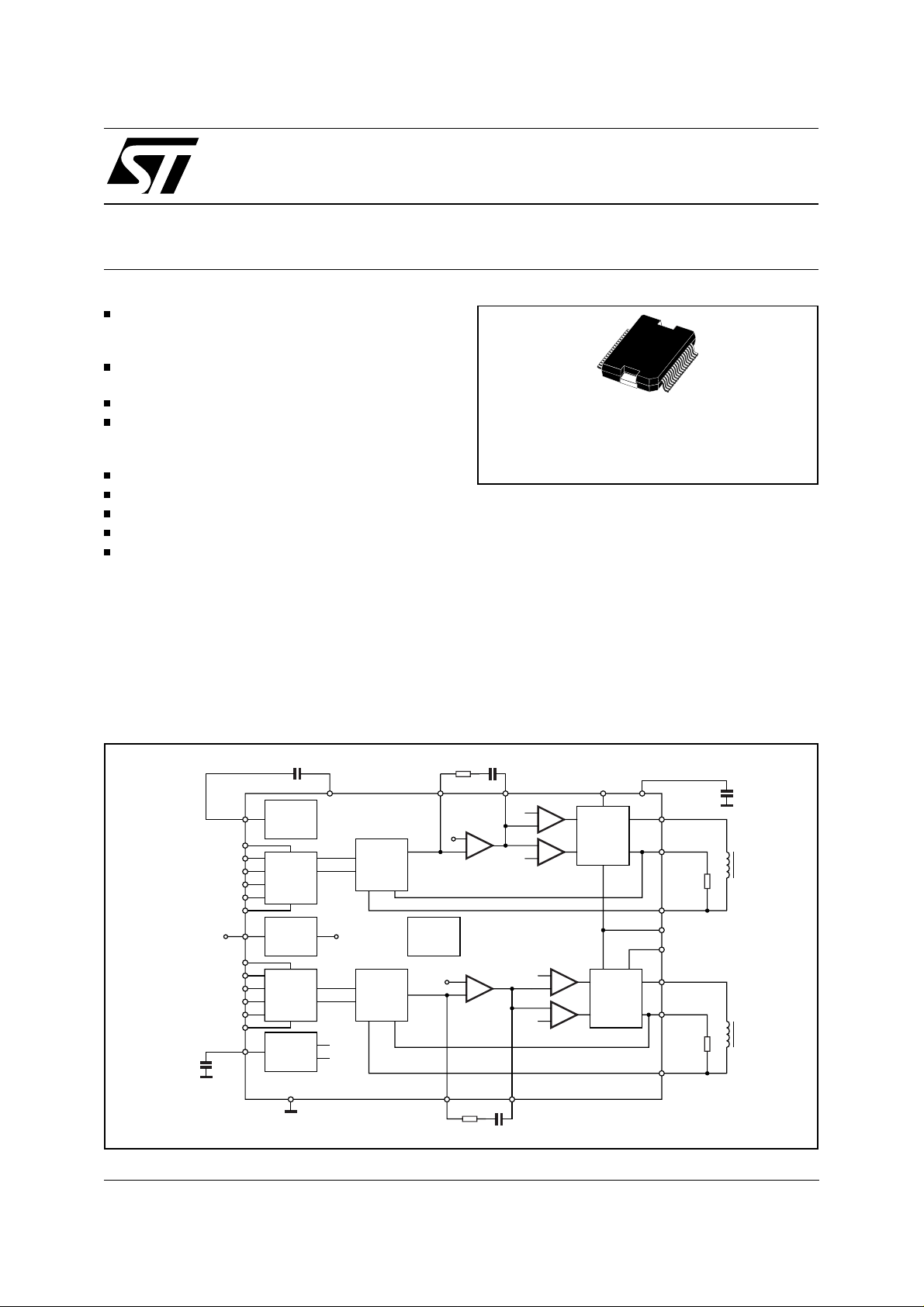
L6258
BLOCK DIAGRAM
C
C2
R
C2
VS
POWER
BRIDGE
1
+
C
-
+
-
BRIDGE
C
POWER
2
VBOOT
D96IN430D
OUT1A
OUT1B
SENSE1B
SENSE1A
DISABLE
VS
OUT2A
OUT2B
SENSE2B
SENSE2A
C
BOOT
R
s
R
s
1/18
INPUT
&
SENSE
AMP
INPUT
&
SENSE
AMP
EA_IN2 EA_OUT2VCP2
THERMAL
PROT.
EA_IN1 EA_OUT1GND
TRI_0
+
TRI_180
C1
TRI_0
TRI_180
C
-
+
C
-
ERROR
V
R
AMP
+
-
ERROR
V
R
AMP
+
-
R
C1
C
VDD(5V)
VCP1
VREF1
I3_1
I2_1
I1_1
I0_1
PH_1
VREF1
I3_2
I2_2
I1_2
I0_2
PH_2
TRI_CAP
C
FREF
C
P
CHARGE
PUMP
DAC
VR GEN
DAC
TRIANGLE
GENERATOR
VR (VDD/2)
TRI_0
TRI_180
April 2000
This is preliminary information on a new product now in development or undergoing evaluation. Details are subject to change without notice.

L6258
ABSOLUTE MAXIMUM RATINGS
Symbol Parameter Value Unit
Vs Supply Voltage 50 V
V
V
ref1/Vref2
I
I
V
V
boot
V
boot - Vs
T
T
CC
O
O
in
j
stg
Logic Supply Voltage 7 V
Reference Voltage 2.5 V
Output Current (peak) 2 A
Output Current (continuous) 1.5 A
Logic Input Voltage Range -0.3 to 7 V
Bootstrap Supply 60 V
Maximum Vgate applicable 15 V
Junction Temperature 150 °C
Storage Temperature Range -55 to 150 °C
PIN CONNECTION
(Top view)
PWR_GND
PH_1
I1_1
I0_1
OUT1A
DISABLE
TRI_CAP
V
CC
GND
VCP1
VCP2
VBOOT
VS
OUT2A
I0_2
I1_2
PH_2
PWR_GND
1
2
3
4
5
6
7
8
9
36
35
34
33
32
31
30
29
28
10 27
11
12
26
25
13 24
14
15
16
17
18
23
22
21
20
19
PWR_GND
SENSE1
OUT1B
I3_1
I2_1
VS
EA_OUT1
EA_IN1
VREF1
SIG_GND
VREF2
EA_IN2
EA_OUT2
I2_2
I3_2
OUT2B
SENSE2
PWR_GND
2/18
D96IN432E

PIN FUNCTIONS
Pin # Name Description
1, 36 PWR_GND Ground connection (1). They also conduct heat from die to printed circuit
2, 17 PH_1, PH_2 These TTL compatible logic inputs set the direction of current flow through
3I
4I
1_1
0_1
5 OUT1A Bridge output connection (1)
6 DISABLE Disables the bridges for additional safety during switching. When not
7 TRI_cap Triangular wave generation circuit capacitor. The value of this capacitor
8V
(5V) Supply Voltage Input for logic circuitry
CC
9 GND Power Ground connection of the internal charge pump circuit
10 V
11 V
12 V
13, 31 V
CP1
CP2
BOOT
S
14 OUT2A Bridge output connection (2)
15 I
16 I
0_2
1_2
18, 19 PWR_GND Ground connection. They also conduct heat from die to printed circuit copper
20, 35 SENSE2, SENSE1 Negative input of the transconductance input amplifier (2, 1)
21 OUT2B Bridge output connection and positive input of the tranconductance (2)
22 I
23 I
1_3
2_2
24 EA_OUT_2 Error amplifier output (2)
25 EA_IN_2 Negative input of error amplifier (2)
26, 28 V
REF2
, V
REF1
27 SIG_GND Signal ground connection
29 EA_IN_1 Negative input of error amplifier (1)
30 EA_OUT_1 Error amplifier output (1)
32 I
33 I
2_1
3_1
34 OUT1B Bridge output connection and positive input of the tranconductance (1)
Note: The number in parenthesis shows the relev ant Power Bridge of the circui t. Pins 18, 19, 1 and 36 are connected together.
copper.
the load. A high level causes current to flow from OUTPUT A to OUTPUT B.
Logic input of the internal DAC (1). The output voltage of the DAC is a
percentage of the Vref voltage applied according to the thruth table of page 7
See pin 3
connected the bridges are enabled
defines the output switching frequency
Charge pump oscillator output
Input for external charge pump capacitor
Overvoltage input for driving of the upper DMOS
Supply voltage input for output stage. They are shorted internally
Logic input of the internal DAC (2). The output voltage of the DAC is a
percentage of the VRef voltage applied according to the truth table of page 7
See pin 15
See pin 15
See pin 15
Reference voltages for the internal DACs, determining the output current
value. Output current also depends on the logic inputs of the DAC and on
the sensing resistor value
See pin 3
See pin 3
L6258
3/18
L6258
THERMAL DATA
Symbol Parameter Value Unit
R
th j-amb
R
th j-case
(*) Depending on board and soldering.
ELECTRICAL CHARACTERISTICS
S
= 42V; VCC = 5V; V
(V
Symbol Parameter Test Condition Min. Typ. Max. Unit
V
S
V
CC
V
BOOT
V
Sense
V
S(off)
V
SH/VCC14
V
CC(off)
I
S(on)
I
S(off)
I
CC (OFF )
T
SD
∆T
SD-H
T
J
f
osc
TRANSISTORS
I
DSS
R
ds(on)
V
f
Thermal Resistance Junction Ambient 20 °C/W
Thermal Resistance Junction-case (*) 2.2 °C/W
boot
= 52V; Tj = 25°; unless otherwise specified.)
Supply Voltage 12 40 V
Logic Supply Voltage 4.75 5.25 V
Storage Voltage VS = 12 to 45V VS+6 VS+12 V
Max Drop Across Sense Resistor 1.25 V
Power on Reset Off Threshold 6 7.2 V
Power on Histeresys 0.3 V
Power on Reset Off Threshold 3.3 4.1 V
VS Quiescent Current Both bridges ON, No Load 15 mA
VS Quiescent Current Both bridges OFF 7 mA
VCC Operative Current DISABLE = LOW 7 mA
Shut Down Temperature 145 °C
Shut Down Hysteresis 25 °C
Thermal Shutdown 150 °C
Triangular Oscillator Frequency (*) C
= TBD 12.5 15 17.5 KHz
FREF
Leakage Current OFF State 500 µA
On Resistance ON State 0.6 0.75 Ω
Flywheel diode Voltage If =1.0A 1 1.4 V
CONTROL LOGIC
V
in(H)
V
in(L)
I
in
I
dis
V
ref1/ref2
I
ref
FI =
V
ref/Vsense
V
FS
V
offset
lnput Voltage All Inputs 2 V
CC
Input Voltage All Inputs 0 0.8 V
Input Current (Note 1) 0 < Vin < 5V -150 +10 µA
Disable Pin Input Current -10 +150 µA
Reference Voltage operating 0 2.5 V
V
Terminal Input Current V
ref
= 1.25 -2 5 µA
ref
PWM Loop Transfer Ratio 2
DAC Full Scale Precision Vref = 2.5V I0/I1/I2/I3 = L 123 134 mV
Current Loop Offset Vref = 2.5V I0/I1/I2/I3 = H -30 +30 mV
DAC Factor Ratio Normalized @ Full scale Value -2 +2 %
SENSE A MPLIFIER
V
cm
I
inp
lnput Common Mode Voltage
-0.7 VS+0.7 V
Range
Input Bias sense1/sense2 -200 0 µA
ERROR AMPLIFIER
G
V
SR Output Slew Rate Open Loop 0.2 V/µs
GBW Gain Bandwidth Product 400 kHz
Note 1: This is true for all the logic inputs except the disable input.
(*) Chopping frequency is twice fosc value.
Open Loop Voltage Gain 70 dB
V
4/18

L6258
FUNCTIONAL DESCRIPTION
The circuit is intended to drive both windings of a
bipolar stepper motor or two DC motors.
The current control is generated through a switch
mode regulation.
With this system the direction and the amplitude
of the load current are depending on the relation
of phase and duty c ycle bet ween the two outputs
of the current control loop.
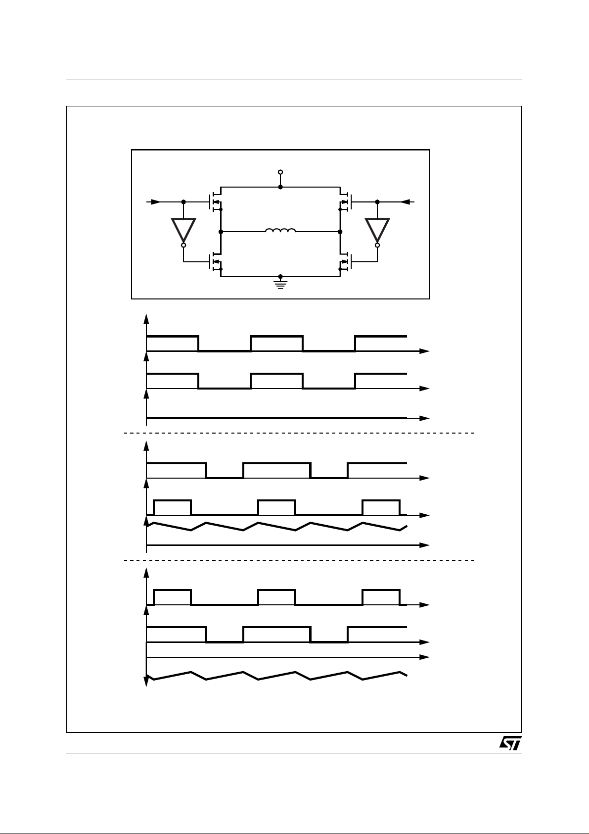
The L6258 power stage is composed by power
DMOS in bridge configuration as it is shown in figure 1, where the bridge outputs OUT_A and
OUT_B are driven to Vs with an high level at the
inputs IN_A and IN_B while are driven to gr ound
with a low level at the same inputs .
The zero current condition is obtained by driving
the two half bridge using signals IN_A and IN_B
with the same phase and 50% of duty cycle.
In this case the outputs of the two half bridges are
continuously switched between power supply (Vs)
and ground, but keeping the differential voltage
across the load equal to zero.
In figure 1A is shown the timing diagram of the
two outputs and the load current for this working
condition.
Following we consider positive the current flowing
into the load with a direction from OUT_A to
OUT_B, while we consider negative the current
flowing into load with a direction from OUT_B to
OUT_A.
Now just increasing the duty cycle of the IN_A
signal and decreasing the duty cycle of IN_B signal we drive positive current into the load.
In this way the two outputs are not in phase, and
the current can flow into the load trough the diagonal bridge formed by T1 and T4 when the output OUT_A is driven to Vs and the output OUT_B
is driven to ground, while there will be a c urrent
recirculation into the higher side of the bridge,
through T1 and T2, when both the outputs ar e at
Vs and a current recirculation into the lower side
of the bridge, through T3 and T4, when both the
outputs are connected to ground.
Since the voltage applied t o the load for recircula-
tion is low, the resulting current discharge time
constant is higher than the current charging time
constant during the period in which the current
flows into the load through the diagonal bridge
formed by T1 and T4. In this way the load current
will be positive with an average amplitude depending on the diff erence in dut y cycle of t he two
driving signals.
In figure 1B is shown the timing diagram in the
case of positive load current
On the contrary, if we want to drive negative current into the load is necessary to decrease the
duty cycle of the IN_A signal and increase the
duty cycle of the IN_B signal. In this way we obtain a phase shift between the two outputs such
to have current flowing into the diagonal bridge
formed by T2 and T3 when the output OUT_A is
driven to ground and output OUT_B is driven to
Vs, while we will have the same current recirculation conditions of the previous case when both
the outputs are driven to Vs or to ground.
So, in this case the load current will be negative
with an average amplitude always depending by
the difference in duty cycle of the two driving signals.
In figure 1C is shown the timing diagram in the
case of negative load current .
Figure 2 shows the device block diagram of the
complete current control loop.
Reference Voltage
The voltage applied to V
pin is the reference
REF
for the internal DAC and, together with the sense
resistor value, defines the maximum current into
the motor winding according to the following relation:
I
MAX
=
0.5 ⋅ V
R
S
REF
=
FI
V
1
REF
⋅
R
S
where Rs = sense resistor value
5/18
L6258
Figure 1.
Power Bridge Configuration
IN_A IN_B
OUTA
OUTB
V
S
T1
OUT_A OUT_B
T3
LOAD
T2
T4
Iload
OUTA
OUTB
Iload
OUTA
OUTB
Iload
Fig. 1A
0
Fig. 1B
0
Fig. 1C
0
D97IN624
6/18

L6258
Figure 2.
VREF
I0
I1
I2
I3
PH
Current Control Loop Block Diagram
INPUT TRANSCONDUCTANCE
VDAC
DAC
AMPL.
+
-
Gin=1/Ra
ia
ERROR AMPL.
V
R
+
ic
Rc
ib
Gs=1/Rb
SENSE TRANSCONDUCTANCE
AMPL.
Cc
-
+
VSENSE
Tri_0
Tri_180
-
+
-
+
POWER AMPL.
VS
OUTA
LOAD
R
L
L
VS
OUTB
D97IN625
L
R
S
Input Logic
(I0 - I1 - I2 - I3)
The current level in the motor winding is selected
according to this table:
I3 I2 I1 I0
H H H H No Current
HHHL 9.5
HHLH 19.1
H H L L 28.6
H L H H 38.1
HLHL 47.6
H L L H 55.6
HLLL 63.5
LHHH 71.4
L H H L 77.8
LHLH 82.5
L H L L 88.9
L L H H 92.1
LLHL 95.2
L L L H 98.4
LLLL 100
Current level
% of I
MAX
Phase Input
( PH )
The logic level applied to this input determines
the direction of the current flowing in the winding
of the motor.
High level on the phase input causes the motor
current flowing from OUT_A to OUT_B through
the load.
Triangular Generator
This circuit generates the two triangular waves
TRI_0 and TRI_180 internally used t o generate
the duty cycle variation of the signals driving the
output stage in bridge configuration.
The frequency of the triangular wave defines the
switching frequency of the output, and can be adjusted by changing the capacitor connected at
TR1_CAP pin :
K
=
F
ref
C
where : K = 2 x 10⁻⁵
7/18

L6258
Charge Pump Circuit
To ensure the correct driving of the high side drivers a voltage higher than Vs is supplied on the
Vboot pin. This boostrap voltage is not needed for
the low side power DMOS transistors because
their sources terminals are grounded. To produce
this voltage a charge pump method is used. It is
made by using two external capacitors; one connected to the internal oscillator (CP) and the other
) to storage the overvoltage needed for the
(C
boot
driving the gates of the high side DMOS. The
value suggested for the capacitors are:
C
boot
C
P
Storage
Capacitor
Pump
Capacitor
100 nF
10 nF
Current Control LOOP
The current control loop is a transconductance
amplifier working in PWM mode.
The motor current is a function of the programmed DAC voltage.
To keep under control the out put current, the cur-
Figure 3. Output comparator waveforms
rent control modulates the duty cycle of the two
outputs OUT_A and OUT_B, and a sensing resistor Rs is connected in series with the motor winding in order to produce a voltage feedback compared with the programmed voltage of the DAC .
The duty cycle modulation of the two outputs is
generated comparing the voltage at the outputs of
the error amplifier, with t he two triangular wave
references .
In order to drive the output bridge with the duty
cycle modulation explained before, the signals
driving each output ( OUTA & OUTB ) are generated by the use of the two comparators having as
reference two triangular wave signals Tri_0 and
Tri_180 of the same amplitude, the same average
value (in our case Vr), but with a 180° of phase
shift each other.
The two triangular wave references are respectively applied to the inverting input of the first
comparator and to the non inverting input of the
second comparator .
The other two inputs of the comparators are connected together to the error amplifier output voltage resulting by the difference between the programmed DAC. The reset of the comparison
between the mentioned signals is shown in fig. 3.
Tri_0
Error Ampl.
Output
Tri_180
First Comp.
Output
Second Comp.
Output
8/18

L6258
In the case of V
equal to zero, the trans con-
DAC
ductance loop is balanced at the value of Vr, so
the outputs of the two comparators are signals
having the same phase and 50% of duty cycle .
As we have already mentioned, in this saturation,
the two outputs OUT_A and OUT_B are simultaneously driven from Vs t o ground ; and the differential voltage across the load in this case is zero
and no current flows in the motor winding.
With a positive differential voltage on V
DAC
(see
Fig 2, the transconductance loop will be positively
unbalanced respected Vr.
In this case being the error amplifier output voltage greater than Vr, the output of the first comparator is a square wave with a duty cycle higher
than 50%, while the output of the second comparator is a square wave with a duty cycle lower
than 50%.
The variation in duty cycle obtained at the outputs
of the two comparators is t he same, but one is
positive and the other is negative with respect to
the 50% level.
The two driving signals, generated in this case,
drive the two outputs in such a way to have
switched current flowing from OUT_A through the
motor winding to OUT_B.
With a negative differential voltage V
, the tran-
DAC
sconductance loop will be negatively unbalanced
respected Vr.
In this case the output of the first comparator is a
square wave with a duty cycle lower than 50%,
while the output of the second comparator is a
square wave with a duty cycle higher than 50%.
The variation in the duty cycle obtained at the outputs of the two comparators is always of the
same.
The two driving signals, generated in this case,
drive the the two outputs in order to have the
switched current flowing from OUT_B through the
motor winding to OUT_A.
Current Control Loop Compensation
In order to have a flexible system able to drive
motors with different electrical characteristics, the
non inverting input and the output of the error amplifier ( EA_OUT ) are available.
Connecting at these pins an external RC compensation network it is possible to adjust the gain
and the bandwidth of the current control loop.
PWM CURRENT CONTROL LOOP
Open Loop Transfer Function Analysis
Block diagram : refer to Fig. 2.
Application data:
VS = 24V Gs transconductance gain = 1/Rb
LL = 12mH Gin transconductance gain = 1/Ra
= 12Ω Ampl. of the Tria_0_180 ref. = 1.6V
R
L
= 0.33Ω Ra = 40KΩ
R
S
RC = to be calculated
C
= to be cal-
C
culated
(peak to peak)
Rb = 20KΩ
Vr = Internal reference equal to
V
/2 (Typ. 2.5V)
CC
these data refer to a t ypical application, and will
be used as an example during the analysis of the
stability of the current control loop.
The block diagram shows the schematics of the
L6258 internal current control loop working in
PWM mode; the current into the load is a function
of the input control voltage V
, and the relation
DAC
between the two variables is given by the following formula:
I
⋅ RS ⋅ GS = V
load
I
⋅ RS
load
I
= V
load
⋅
DAC
1
R
⋅
= V
b
Ra ⋅ R
R
DAC
DAC
b
⋅ G
⋅
= 0.5
S
in
1
R
a
V
DAC
⋅
R
S
(A
)
where:
V
DAC
is the control voltage defining the
load current value
G
in
is the gain of the input transconductance amplifier ( 1/Ra )
G
s
is the gain of the sense transconductance amplifier ( 1/R
)
b
Rs is the resistor connected in series
to the output to sense the load
current
In this configuration the input voltage is compared
with the feedback voltage coming from the sense
resistor, then the difference between this two signals is amplified by the error amplifier in order to
have an error signal controlling the duty cycle of
the output stage keeping the load current under
control.
It is clear that to have a good performance of the
current control loop, the error amplifier must have
an high DC gain and a large bandwidth .
Gain and bandwidth must be chosen depending
on many parameters of the application, like the
characteristics of the load, power supply etc...,
and most important is the stability of the system
that must always be guaranteed.
To have a very flexible system and to have the
possibility to adapt the system to any application,
the error amplifier must be compensated using an
9/18

L6258
RC network connected between the output and
the negative input of the same.
For the evaluation of the stability of the system,
we have to consider the open loop gain of the
current control loop:
Aloop = ACerr ⋅ ACpw ⋅ ACload ⋅ ACsense
where AC... is the gain of the blocks that refers to
the error, power and sense amplifier plus the attenuation of the load block.
The same formula in dB can be written in this
way:
AloopdB = ACerrdB + ACpwdB + ACloaddB + ACsense
dB
So now we can start to analyse the dynamic characteristics of each single block, wit h particular attention to the error amplifier.
Power Amplifier
The power amplifier is not a linear amplifier, but is
a circuit driving in PWM mode the output stage in
full bridge configuration.
The output duty cycle variation is given by the
comparison between the voltage of the error amplifier and two triangular wave references Tri_0
and Tri_180. Because all the current control loop
is referred to the Vr reference, the result is that
when the output voltage of the error amplifier is
equal to the Vr voltage the two output Out_A and
Out_B have the same phase and duty cycle at
50%; increasing the output voltage of the error
amplifier above the Vr voltage, the duty cycle of
the Out_A increases and the duty cycle of the
Out_B decreases of the same percentage; on the
contrary decreasing the voltage of the error amplifier below the Vr voltage, the duty cycle of the
Out_A decreases and the duty cycle of the Out_B
increases of the same percentage.
The gain of this block is defined by the amplitude
of the two tr iangular wave references; more precisely the gain of the power amplifier block is a reversed proportion of the am plitude of the two references.
In fact a variation of the error amplifier output voltage produces a larger variation in duty cycle of
the two outputs Out_A and Out_B in case of low
amplitude of the two triangular wave references.
The duty cycle has the max value of 100% when
the input voltage is equal to the amplitude of the
two triangular references.
The transfer function of this block consist in the
relation between the output duty cycle and the
amplitude of the triangular references.
V
= 2 ⋅ VS ⋅ (0.5 - DutyCycle)
out
ACpw
= 20 ⋅ log
dB
ACpw|dB = 20 ⋅ log
∆V
∆V
out
=
in
2
2 ⋅ V
S
Triangular Amplitude
⋅ 24
29.5dB
=
1.6
Moreover, having the two references Tri_0 and
Tri_180 a triangular shape it is clear that the
transfer function of this block is a linear constant
gain without poles and zeros.
Load Attenuation
The load block is composed by the equivalent circuit of the motor winding (resistance and inductance) plus the sense resistor.
We will considered the effect of the Bemf voltage
of the motor in the next chapter.
The input of this block is the PWM voltage of the
power amplifier and as output we have the voltage across the sense resistor produced by the
current flowing into the m otor winding. The relation between the two variable is :
V
out
⋅
V
sense
=
RL + R
R
S
S
so the gain of this block is:
ACload
=
ACloaddB
ACloaddB
V
=
=
sense
V
out
20
20
=
R
⋅
log
⋅
log
R
S
+
R
L
S
R
S
R
+ R
L
S
0.33
12 + 0.33
= −
31.4dB
where:
R
= equivalent resistance of the
L
motor winding
R
= sense resistor
S
Because of the inductance of the motor LL, the
load has a pole at the frequency :
Fpole
Fpole
=
=
2π ⋅
6.28
1
L
L
RL + R
1
12 ⋅ 10
⋅
+ 0.33
12
S
=
163Hz
−
3
Before analysing the error amplifier block and the
sense transconductance block, we have to do this
consideration :
10/18

L6258
AloopdB = AxdB + Bx
Ax|dB = ACpw|dB + ACload|
dB
dB
and
= ACerr|dB + ACsense|
Bx|
dB
dB
this means that Ax|dB is the sum of the power amplifier and load blocks;
= (29,5) + (-31.4) = -1.9dB
Ax|
dB
The BODE analysis of the transfer function of Ax
is:
The Bode plot of t he Ax|
function shows a DC
dB
gain of -1.9dB and a pole at 163Hz.
It is clear now that (because of the negative gain
of the Ax function), Bx function must have an high
DC gain in order to increment the total open loop
gain increasing the bandwidth too.
Error Amplifier and Sense Amplifier
As explained before the gain of these two blocks
is :
= ACerrdB + ACsense
Bx
dB
dB
Being the voltage across the sense resistor the
input of the Bx block and the error amplifier voltage the output of the same, the voltage gain is
given by :
ib = Vsense ⋅ Gs = Vsense ⋅
Verr_out = -(ic ⋅ Zc) so ic = -(Verr_out ⋅
1
Rb
1
Zc
)
because ib = ic we have:
Bx =
Verr_out
−
Vsense
= −
Zc
Rb
In the case of no external RC network is used to
compensate the error amplifier, the typical open
loop transfer function of the error plus the sense
amplifier is something with a gain around 80dB
and a unity gain bandwidth at 400kHz. In this
case the situation of the total transfer function
Aloop, given by the sum of the Ax
and BxdB is :
dB
The BODE diagram shows together the error amplifier open loop transfer function, the Ax function
and the resultant total Aloop given by the following equation :
Aloop
= AxdB + Bx
dB
dB
The total Aloop has an high DC gain o f 78.1dB
with a bandwidth of 15KHz, but the problem in
this case is the stability of the system; in fact the
total Aloop cross the zero dB axis with a slope
of -40dB/decade.
Now it is ne cessary to compensate the err or amplifier in order to obtain a total Aloop with an high
DC gain and a large bandwidth. Aloop must have
enough phase margin to guarantee the stability of
the system.
A method to reach the stability of the system, using the RC network showed in the block diagram,
is to cancel the load pole with the zero given by
the compensation of the error amplifier.
The transfer function of the Bx block with the
compensation on the error amplifier is :
1
j
π ⋅
⋅
2
f
Cc
Rb
Bx =
−
Zc
−
Rb
Rc
= −
In this case the Bx block has a DC gain equal to
the open loop and equal to zero at a frequency
given by the following formula :
Vsense ⋅
1
= -(Verr_out ⋅
Rb
1
Zc
)
Fzero =
π ⋅
2
1
Rc ⋅ Cc
11/18

L6258
In order to cancel the pole of the load, the zero of
the Bx block must be located at the same frequency of 163Hz; so now we have to find a compromise between the resistor and the capacitor of
the compensation network.
Considering that the resistor value defines the
gain of the Bx block at the zero frequency, it is
clear that this parameter will influence the total
bandwidth of the system because, annulling the
load pole with the error amplifier zero, the slope
of the total transfer function is -20dB/decade.
So the resistor value must be chosen in order to
have an error amplifier gain enough to guarantee
a desired total bandwidth .
In our example we fix at 35dB the gain of the Bx
block at zero frequency, so from the formula:
Bx_gain
@zero freq.
= 20 ⋅ log
we have : Rc = 1.1M
Rc
where: Rb = 20K
Rb
Ω
Ω
Therefore we have the zero with a 163Hz the capacitor value :
Cc =
1
π ⋅ Fzero ⋅ Rc
2
=
6.28
⋅
163
1
⋅ 1.1 ⋅ 10
= 880pF
6
Now we have to analyse how the new Aloop
transfer function with a compensation network on
the error amplifier is.
The following bode diagram shows :
- the Ax function showing the position of the load
pole
- the open loop transfer function of the Bx block
- the transfer function of the Bx with the RC com-
pensation network on the error amplifier
- the total Aloop transfer function that is the sum
of the Ax function plus the transfer
function of the compensated Bx block.
We can see that the effect of the load pole is cancelled by the zero of the Bx block ; the total Aloop
cross a the 0dB axis with a slope of -20dB/decade, having in this way a stable system with an
high gain at low frequency and a bandwidth of
around 8KHz.
To increase the bandwidth of the system, we
should increase the gain of the Bx block, keeping
the zero in the same position. In this way t he result is a shift of the total Aloop transfer function up
to a greater value.
Effect of the Bemf of the stepper motor on the
current control loop stability
In order to evaluate what is the effect of the Bemf
voltage of the stepper motor we have to look at
the load block :
OUT+
Bemf
R
L
L
L
R
S
OUT-
to Sense
Amplifier
The schematic now shows the equivalent circuit
of the stepper motor including a sine wave voltage generator of the Bemf. The Bemf voltage of
the motor is not constant, its value changes depending on the speed of the motor.
Increasing the motor speed the Bemf voltage increases :
Bemf = Kt
⋅ ω
where:
Kt is the motor constant
ω
is the motor speed in radiant per second
12/18
The formula defining the gain of the load considering the Bemf of the stepper motor becomes:
R
S
RL + R
S
ACload =
ACload =
Vsense
Vout
−
Bemf
V
S
V
S
=
(
V
− Bemf) ⋅
S
R
⋅
RL
V
S
S
+
R
S

ACloaddB
=
20
⋅ log
V
− Bemf
S
V
S
⋅
RL + R
R
S
S
we can see that the Bemf influences only the gain
of the load block and does not introduce any
other additional pole or zero, so from the stability
point of view the effect of the Bemf of the motor is
not critical because the phase margin remains the
same.
Practically the only effect of the Bemf is to limit
the gain of the total Aloop with a consequent variation of the bandwidth of the system.
APPLICATION IN FOR MATION
A typical application circuit is shown in Fig.4.
Note: For avoid current spikes on falling edge of
DISABLE a "DC reaction" would be added
to the ERROR Amplifie r. (R1-R2 on F ig. 4).
Interference
Due to the fact that the circuit operates with
switch mode current regulation, to reduce the effect of the wiring inductance a good capacitor
(100nF) can be placed on the board near the
Figure 4:
Typical Application Circuit.
L6258
package, between the power supply line (pin
13,31) and the power ground (pin 1,36,18,19) to
absorb the small amount of inductive energy.
It should be noted that this capacitor is usually required in addition to an electrolytic capacitor, t hat
has poor performance at the high frequencies, always located near the package, between power
supply voltage (pin 13,31) and power ground (pin
1,36,18,19), just to have a current recirculation
path during the fast current decay or during the
phase change.
The range value of this capacitor is between few
µ
F and 100µF, and it must be chosen depending
on application parameters like the motor inductance and load current amplitude.
A decoupling capacitor of 100nF is suggested
also between the logic supply and ground.
A non inductive resistor is the best way to implement the sensing. Whether this is not possible,
some metal film resistor of the same value can be
paralleled.
The two inputs for the sensing of the winding motor current (SENSE_A & SENSE_B) should be
connected directly on the sensing resistor Rs terminals, and the path lead between the Rs and the
two sensing inputs should be as short as possible.
10nF
100nF
1nF
VCP1
VCP2
VBOOT
GND
TRI_CAP
I0_1
I1_1
I2_1
I3_1
PH2
I0_2
I1_2
I2_2
I3_2
DISABLE
EA_IN1
OUT2B
SENSE2
OUT2A
SENSE1
OUT1B
OUT1APH1
VS
PWR_GND
V
DD
SIG_GND
VREF1
VREF2
0.33
0.33
D97IN626D
M
VS
VDD(5V)
VREF
STEPPER
MOTOR
12mH 10Ω
13,31
18,19
820pF
21
20
14
35
34
5
1,36
8
27
28
26
24
10
11
12
9
7
L6258
2
4
3
32
33
17
15
16
23
22
6
29
EA_OUT1
1M
820pF
SOP36
PACKAGE
30
EA_IN2
25
EA_OUT2
1M
R2 1MR1 1M
13/18

L6258
Motor Sele ctio n
Some stepper motor have such high core losses
that t hey are not suitable for switch mode cur rent
regulation. Furthermore, some stepper motors are
not de sign ed for c ont in uous oper at in g at maxi mum
curren t. Since the cir cuit can drive a constant current through the motor, its temperature might exceed, bo t h at low and high s peed operation.
Unused Inputs
Unused inputs should be connected to the proper
voltage levels in order to get the highest noise immunity.
OPERATION MODE TIME DIAGRAMS
Figure 5:
Full step operation mode timing diagram (Phase - DAC input and Motor Current)
Position
Phase
1
Phase
2
DAC 1
Inputs
DAC 2
Inputs
Motor drive
Current 1
Motor drive
Current 2
5V
0
5V
0
5V
I0_1
0
5V
I1_1
0
5V
I2_1
0
5V
I3_1
0
5V
I0_2
0
5V
I1_2
0
5V
I2_2
0
I3_2
0
0
0
Notes on PCB Design
We recommend to observe the following layout
rules to avoid application problems with ground
and anomalous recirculation current.
The by-pass capacitors for the power and logic
supply must be kept as near as possible to the IC.
It’s important to separate on the PCB board the
logic and power grounds and the internal charge
pump circuit ground avoiding that ground traces
of the logic signals cross the ground t races of the
power signals.
Because the IC uses the board as a heat sink, the
dissipating copper area must be sized in accordance with the required value of R
023103210
Ph2
95.2%
19.1%
95.2%
19.1%
D97IN629A
FULL Step Vector
Ph1
1
Ph1
I3 I2 I1 I0
0000 100
0001 98.4
0010 95.2
0011 92.1
0100 88.9
0101 82.5
0110 77.8
0111 71.4
1000 63.5
1001 55.6
1010 47.6
1011 38.1
1100 28.6
1101 19.1
1110 9.5
1 1 1 1 No Current
Current level
thj-amb
0
32
% of I
.
Ph2
MAX
14/18

L6258
Figure 6:
Phase
1
Phase
2
DAC 1
Inputs
DAC 2
Inputs
Motor drive
Current 1
Motor drive
Current 2
Half step operation mode timing diagram (Phase - DAC input and Motor Current)
I0_1
I1_1
I2_1
I3_1
I0_2
I1_2
I2_2
I3_2
5V
5V
5V
5V
5V
5V
5V
5V
5V
07465213067451320Position
0
0
Ph2
0
0
0
0
0
0
0
0
0
0
D97IN627B
4
95.2%
19.1%
95.2%
19.1%
Half Step Vector
Ph1
2
3
5
6
Ph1
I3 I2 I1 I0
0000 100
0001 98.4
0010 95.2
0011 92.1
0100 88.9
0101 82.5
0110 77.8
0111 71.4
1000 63.5
1001 55.6
1010 47.6
1011 38.1
1100 28.6
1101 19.1
1110 9.5
1 1 1 1 No Current
Current level
% of I
1
Ph2
0
7
MAX
15/18

L6258
Figure 7:
Position
Phase
1
Phase
2
DAC 1
Inputs
DAC 2
Inputs
Motor drive
Current 1
Motor drive
Current 2
4 bit microstep operation mode timing diagram (Phase - DAC input and Motor Current)
I0_1
I1_1
I2_1
I3_1
I0_2
I1_2
I2_2
I3_2
5V
5V
5V
5V
5V
5V
5V
5V
5V
24 28201612840
32
0
0
0
0
0
0
0
0
0
0
0
0
60 64565248444036
Micro Step Vector
Ph1
16
8
56
Ph2
24
32
40
48
Ph1
I3 I2 I1 I0
Current level
% of I
MAX
0000 100
0001 98.4
0010 95.2
100%
95.2%
82.5%
63.5%
47.6%
38.1%
19.1%
0%
0011 92.1
0100 88.9
0101 82.5
0110 77.8
0111 71.4
1000 63.5
1001 55.6
1010 47.6
1011 38.1
1100 28.6
1101 19.1
1110 9.5
1 1 1 1 No Current
Ph2
0
16/18
D97IN628A

L6258
DIM.
MIN. TYP. MAX. MIN. TYP. MAX.
mm inch
A 3.60 0.141
a1 0.10 0.30 0.004 0.012
a2 3.30 0.130
a3 0 0.10 0 0.004
b 0.22 0.38 0.008 0.015
c 0.23 0.32 0.009 0.012
D (1) 15.80 16.00 0.622 0.630
D1 9.40 9.80 0.370 0.385
E 13.90 14.50 0.547 0.570
e 0.65 0.0256
e3 11.05 0.435
E1 (1) 10.90 11.10 0.429 0.437
E2 2.90 0.114
E3 5.80 6.20 0.228 0.244
E4 2.90 3.20 0.114 0.126
G 0 0.10 0 0.004
H 15.50 15.90 0.610 0.626
h 1.10 0.043
L 0.80 1.10 0.031 0.043
N10°(max.)
S8°(max.)
(1): "D" and "E1" do not include mold flash or protrusions
- Mold flash or protrusions shall not exceed 0.15mm (0.006 inch)
- Critical dimensions are "a3", "E" and "G".
OUTLINE AND
MECHANICAL DATA
PowerSO36
NN
a2
A
1936
0.12 AB
⊕
e
M
E1
DETAIL B
lead
a3
B
Gage Plane
PSO36MEC
BOTTOM VIEW
DETAIL B
0.35
S
E
DETAIL A
L
E2
DETAIL A
118
h x 45˚
A
e3
H
D
b
c
a1
slug
E3
D1
- C -
SEATING PLANE
GC
(COPLANARITY)
17/18

L6258
Information furnishe d is beli eved to be accu rate and reliable. However, STMicroelec tronics assumes no res ponsibility for the consequences
of use of such i nformation nor for any i nfringement of patents or ot her rights of third par ties which may result from its use. No license i s
granted by impli cation or otherwis e under any patent or patent righ ts of STMicroelect ronics. Specifica tion mentioned in this publication are
subject to change without notic e. This public ation supers edes and replaces all information prev iously supplied. STMic roelec tronic s products
are not authorized for use as critical components in life support devices or systems without express written approval of STMicroelectronics.
The ST logo is a registered trademark of STMicroelect roni cs
© 2000 STMicroelectronics – Printed in Italy – All Rights Reserved
STMicroelectronics GROUP OF COMPANIES
Australia - Brazil - Canada - China - France - Germany - Italy - Japan - Korea - Malaysia - Malta - Mexico - Morocco - The Netherlands -
Singapore - Spain - Sweden - Switzerland - Taiwan - Thailand - United Kingdom - U.S.A.
http://www.st.com
18/18
 Loading...