

Page 1
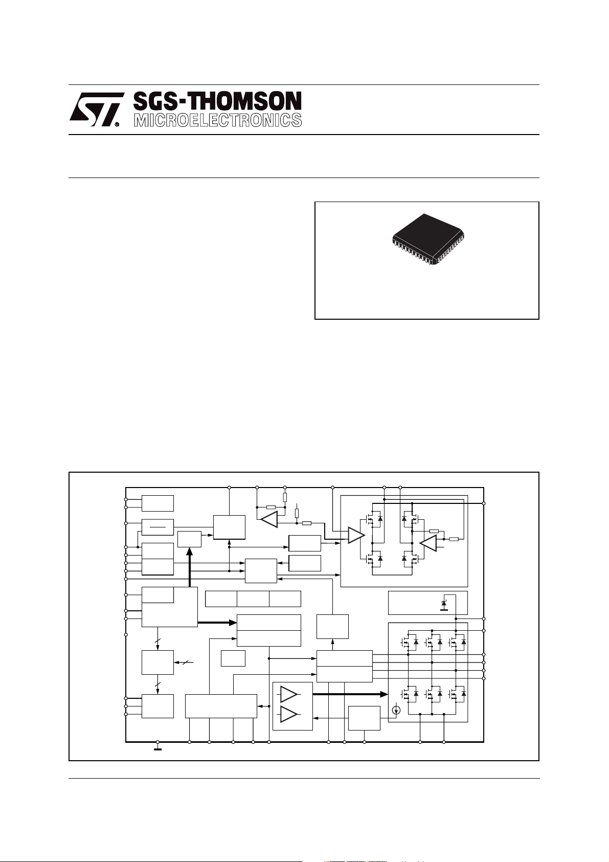
DESCRIPTION
The 12 Volt Combo chip is a combination spindle
motor driver, voice coil driver and D/A converter.
The part can be used in,application like HDD.
The VCM amplifiers drive a low impedance coil
and are set up to accept RC compensation, which
allows a wide bandwidth with absolute minimum
phase lag. The sense resistor/amplifier arrangement allows full current loop operation. The loop
gain is changeable by attenuating the VCM DAC
voltage amplitude in cascadable stages.
The Spindle driver is a PWM only voltage loop
with power supply feedforward, driving a 3 phase
sensorless brushless DC motor. Since it uses
PWM operation at full run speed, it has output
slew rate control during start and run modes.
There is an inductive clamp circuit to limit flyback
voltage transients across the supply voltage during motor phase changes and during the braking
sequence. Only the 2 phase or bipolar commutation pattern is produced by the internal commutation circuitry. A commutation register allows arbi-
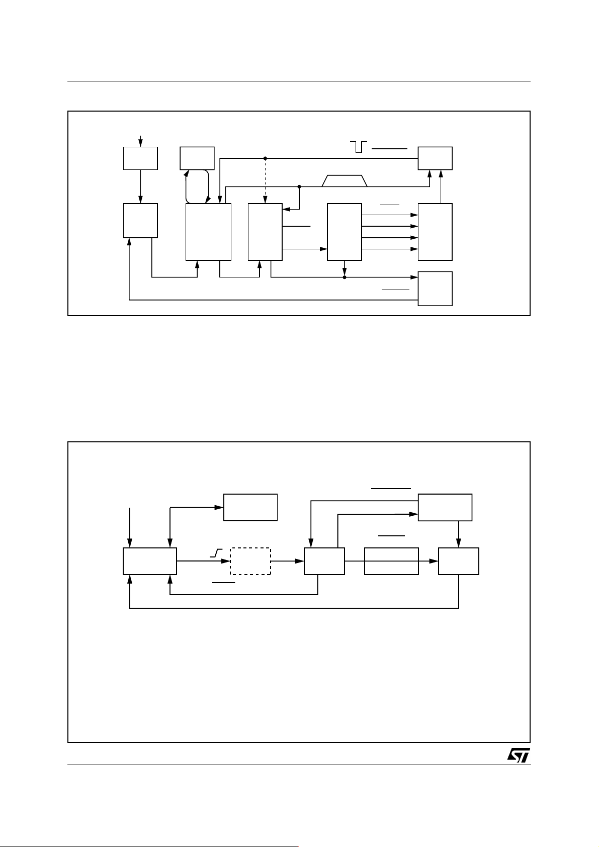
Figure 1. Block Diagram
L6256
12V COMBO
PLCC44
ORDERING NUMBER:
trary winding sequencing during certain operations. Internal protection against crossover
spikes is built in.
3 phase or tripolar commutation can be supported
in software during start by writing a commutation
pattern directly to the preload register.
Tripolar operation requires that more than two
phase drivers contribute current simultaneously.
The current limit circuitry reflects this and allows
33% higher current limit, which produces nearly
L6256
CP_OUT
CP_CAP
H_VPWR
VDD
VCC
nPOR
POR_RC
PARK
SCLK
SDIO
CSELB
BYPASSC
QDRIVE
VREG_IN
CUR_IN
December 1997
18
19
33
34
15
10
9
27
13
14
28
16
20
21
22
3.3V LINEAR
REGULATOR
6,7,17,29,39,40
CHARGE
PUMP
VPWR
2
UV
DETECT
POR
CLK
SYNC
SERIAL INTERFACE
3
ANALOG
TEST MUX
3
VCM
LOGIC
h_vpwr
BRAKE
DELAY
COUNTER
SH_
OUT
A_INI_VCIO_VC
BEMF SENSING
ZERO CROSSING
DETECTION
BEMF_
DET
DAC
VCM
COMMAND
10 BIT
DAC
8 11 36 37 5 38 12 35 44 4
R_
SLEW
CHANNEL
VCM CONTROL
BANDGAP
24
FEEDFORWARD
COMPENSATION
PWM_INPWM_DCFF_
VOLTAGE
REFERENCE
SPINDLE SEQUENCER
SYNC
CLAMP
COMP
VCM
RETRACT
CURRENT
SOURCES
SPINDLE LOGIC
SP_
CLK
THERMAL
upper
lower
PRE-DRIVERS
VCM CLASS AB
DRIVERS
-
+
A
AMP
CURRENT
LIMIT
SENSING
REF_
IN
A_OUT B_OUT
232530263132
PWR GND
SPINDLE DRIVERS
DYNAMIC
CLAMPING
SP_G2SP_
AMP
B
24
VC_PWR
-
+
h_vpwr
2
SP_P1
42
SP_P2
43
SP_A
1
SP_B
3
SP_C
41
C_TAP
D97IN571
G1
1/28
Page 2
L6256
DESCRIPTION
(Continued)
constant torque. This is a very high power dissipation mode, meant only for momentary operation in unusual circumstances.
Spindown during a power failure uses the back
EMF voltage generated by the spindle motor to
provide power to the VCM amplifier. The Spindle
motor coasts during the Brake Delay time to allow
time to park the head actuator. The park circuit is
a constant voltage circuit settable externally.
After the head is parked, braking commences.
The brake operates by shorting all 3 windings.
required to bring the motor to a complete stop,
even if no power is applied to the part.
A Power On Reset (POR) function provides pulse
stretching for the bidirectional POR\ bus, to ensure that the processor and clocks are at running
speed before allowing them to function.
5 volt and 12 volt pins are used directly for the undervoltage detect circuit.
This allows direct use internally of both supplies.
Voltage monitor margining is supported.
An external 3.3V linear regulator is provided and
tied into the POR circuit.
The spindle output stages stay on as long as is
OPERATING CONDITIONS
= 4.5 to 5.5V
V
CC
= 10.8 to 13.2V
V
dd
0°C < T
amb
< 70°C.
ABSOLUTE MAXIMUM RATINGS
Symbol Parameter Value Unit
V
PWR
V
PVR
V
dd
V
CC
I_VCM, Aout -2 to V
Logic I/O, SH_Out, PWM_DC -0.3 to V
All other pins -0.3 to V
T
stg
(1) Limited by chip clamp voltage.
Normal Operating Voltage 15 V
Inductive Clamp Voltage @ 2mH, 1.6A, 3% Duty Cycle <20 V (1)
Storage Ambient Temperature -65 to +150 °C
ESD capability
15 V
6.4 V
+2V
PWR
+0.3
CC
+0.3V
PWR
2kV
±
PIN CONNECTION
2/28
GND
R_SLEW
POR_RC
nPOR
PWM_IN
BEMF_DET
SCLK
SDIO
VCC
BYPASSC
5V_GND
7
8
9
10
11
12
13
14
15
16
17
SP_CLK
GND
CP_CAP
CP_OUT
SP_C
SP_G1
QDRIVE
VREG_IN
SP_B
SP_P1
123564
2322211918 20 28272624 25
B_OUT
CUR_IN
SP_G2
SP_A
A_OUT
VC_PWR
C_TAP
SP_P2
I_VC
PARK
GND
40414244 43
CSELB
39
38
37
36
35
34
33
32
31
30
29
GND
SH_OUT
FF_COMP
PWM_DC
REF_IN
VDD
H_VPWR
DAC
IO_VC
A_IN
GND
D97IN572
Page 3
THERMAL DATA
Symbol Description Value Unit
R
th j-pins
R
th j-amb
(*) Mounted on board with minimized dissipating copper area.
Thermal Resistance Junction-pins
Thermal Resistance Junction-ambient (*)
Max.
Max.
12
50
PIN DESCRIPTION
Pin # Pin Name Pin Description Type
1 SP_B Spindle Output, Ph B Power/Output
2, 42 SP_P1, SP_P2 Spindle driver Supply Power/Input
3 SP_C Spindle Output, Ph C Power/Output
4,44 SP_G1,SP_G2 Spindle Driver Ground Power/Output
5 SP_CLK Spindle Clock Input Cmos/Input
6,7,29,39,40 GND Power Ground Ground/Heatsink
8 R_SLEW Spindle Slew/FeedFwd Osc. Freq. Analog/Input
9 POR_RC Ext. POR Timing Cap. Analog/Output
10 nPOR POR Reset (Active LOW) Cmos/BIO
11 PWM_IN Spindle PWM Input Cmos/Input
12 BEMF_DET Spindle BEMF Output Cmos/Output
13 SCLK Serial Data Clock Cmos/Input
14 SDIO Bidirectional Serial Data I/O Cmos/BIO
15 VCC 5V Digital Supply Supply/Input
16 BYPASSC Not to be used -
17 5V_GND 5V Supply Ground Ground/Output
18 CP_OUT Charge Pump Pumping Cap Analog/Output
19 CP_CAP Charge Reservoir Cap Analog/Input
20 QDRIVE 3.3V Regulator Base Drive Analog/Output
21 VREG_IN 3.3V Regulator Voltage Feedback Analog/IO
22 CUR_IN 3.3V Regulator Current Feedback Analog/IO
23 B_OUT VCM Driver Output, B Power/Output
24 VC_PWR VCM Drivers Supply Power/Input
25 A_OUT VCM Driver Output, A Power/Output
26 I_VC VCM Sense Amplifier Input Analog/Input
27 PARK VCM Park Pin Analog/Input
28 CSELB Chip Select -
30 A_IN VCM A-Amplifier Input Analog/Input
31 IO_VC VCM Sense Amplifier Output Analog/Output
32 DAC VCM DAC Command Output Analog/Output
33 H_VPWR VCM Vpwr/2 Reference Voltage Analog/Output
34 VDD 12V Analog Supply Supply/Input
35 REF_IN Spindle Current Limit/Win Threshd Analog/Input
36 PWM_DC Spindle Filtered PWM Input Analog/Input
37 FF_COMP Spindle Feedforwd Ramp Generator Analog/Input
38 SH_OUT Spindle BEMF Sample/Hold Analog/Output
41 C_TAP Spindle Centre Tap Analog/Input
43 SP_A Spindle Output, Ph A Power/Output
L6256
C/W
°
C/W
°
3/28
Page 4
L6256
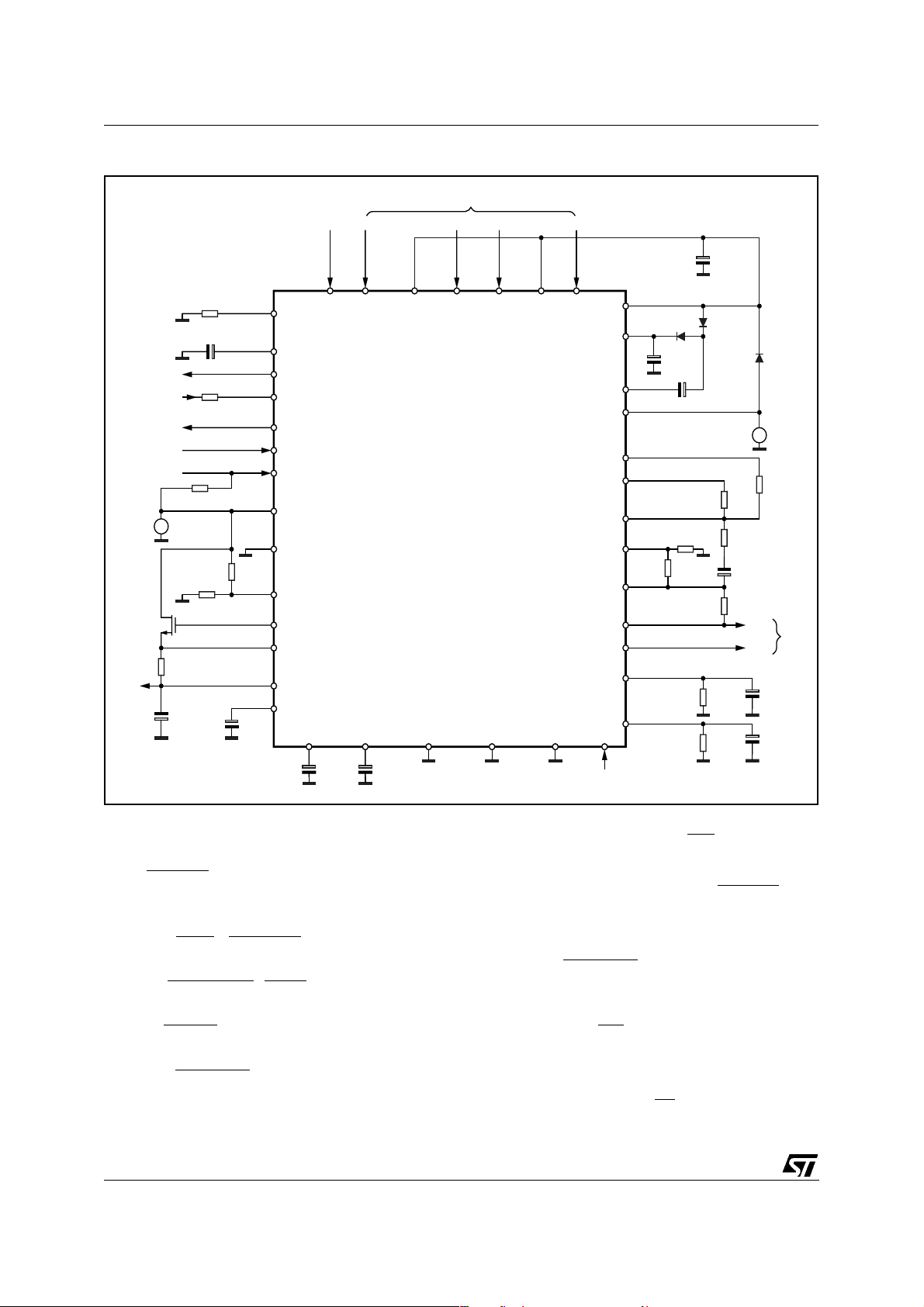
TYPICAL APPLICATION DIAGRAM
SP_CLK SP_C SP_B SP_A C_TAP
SP_C SP_B SP_A C_TAP
SP_CLK
5
33
H_VPWR
BEMF_DET
V
3.3V
C3
22µF
esr 0.5Ω
nPOR
PWM
SCLK
SDIO
CC
R
1.5Ω
S
+
V
-
R
SLEW
100KΩ
C2 47nF
R
PWM
33KΩ
RDIO 1.2KΩ
R
REF2
R
REF
62.5KΩ
Cbyp
10nF
R_SLEW
POR_RC
nPOR
PWM_IN
BEMF_DET
SCLK
SDIO
VCC
5V_GND
120KΩ
REF_IN
QDRIVE
CUR_IN
VREG_IN
BYPASSC
C
HVPWR
100nF
8
9
10
11
12
13
14
15
17
35
20
22
21
16
37
FF_COMP
SP_P1
C
ffc
470pF
SPINDLE
vpwr
C1
4.7µF
D4
33nF
51KΩ
p1
R
p2
100KΩ
R
sh
pwindc
25V
D5
D1
+
V
V
DD
-
R
b
4.3KΩ
R
a
1.5KΩ
R
fb
120KΩ
C
fb
390pF
R
SENSE
0.75Ω
I_VC
VCM
B_OUT
C
sh
3.3nF
C
dc
10nF
SP_P2
414313
SP_G2
42
6,7,29,39,40
GND
CSelB (from µP)
2
4
SP_G1
44
28
24
19
18
34
32
31
30
27
25
26
23
38
36
CSELB
VC_PWR
CP_CAP
CP_OUT
VDD
DAC
IO_VC
A_IN
PARK
A_OUT
I_VC
B_OUT
SH_OUT
PWM_DC
C
PCAP
2.2µF
35V
C
POUT
R
100KΩ
R
100KΩ
D97IN573
DESIGN FORMULAS:
1.
Spindle Run Mode Slew Rate:
1500 ⋅ 10
SR
=
2.
Feedforward Compensation:
Fpwm =
Dout =
=
V
ref
Vrslew =
Fpwm = PWM chopping frequency
Din = Input duty cycle at pwm_in
Dout = Spindle output duty cycle
4/28
Rslew
1
Tpwm
Tpwm
Tpwm
Rpwmdc
Rpwm
Vpwr
(
3
(Volts
=
Cffc
+ 0.7µs
⋅ 2.47 (V
0.8
+
1.86
/µs
)
(V
⋅
⋅
)
1
Rslew
Vref
Vrslew
)
)
(
Hz
⋅
Din
Vcc
3.
Current Limit: Ilimit = 20 ⋅ 10
4.
BEMF Zero Crossing Detector:
- Slope Compensation: Csh ⋅ Rsh =
Vbemf = Amplitude of bemf
3
(A
⋅
Rref
)
5.9683
Vbemf
⋅ N
(sec
)
N = Run mode speed of the motor in RPM
)
- Window width:
t
= 15404
win
5.
VCM PARKING VOLTAGE:
V
= 0.5
A,park
6.
3.3V REGULATOR:
Max Load Current: I
Vcc ⋅ Rref
⋅
Rref
1 +
⋅
Rref2
+
Rp2
Rp1
MAX
⋅ Vbemf ⋅ N
V
)
(
0.3
=
Rs
Polepair (µs
⋅
(A)
)
Page 5

L6256
GENERAL BLOCK DESCRIPTIONS
(see figure 1)
Charge Pump
The Charge Pump provides bias for the upper drivers, for the brake circuit, and for internal circuitry as
required for normal and spindown operation. Slew
rate control is built in for quiet operation.
Serial Interface
The serial interface will transfer all control, status
and data to and from the processor. Internal testing provisions have also been made through this
port. The interface is compatible with an
8X196MP,NU or K17 series processor at low
speed only, due to internal limitations of the processors. External chip select is mandatory on the
L6256. Chip Select is also used to reset and synchronize the serial port. The serial port is used to
indicate thermal shutdown of the Dolphin chip.
Brake Delay Timer
The brake delay will, upon start of a park or brake
sequence, delay 128 negative zero crossings of
the A spindle phase to allow the park circuit to operate. (The delay will typically be on the order of
400 msecs.) Then the braking sequence can begin. The output of this timer is provided to the serial port registers to indicate the start of the brake
action, and to indicate the start and end of the
park period.
Spindle Section
SPINDLE CURRENT LIMIT
The spindle current limit value in start mode is set
by the value of the external resistor on the Ref_In
pin during start (which at start is shorted to Vcc,
and the current out of the pin sets the current limit
value).
During run, various internal methods are used to
set a nominal maximum current value for circuit
protection only. Consult the data sheets and application notes for a description of this circuitry.
Current limit operates on a cycle by cycle basis.
The current limit comparator output is provided to
the serial port to indicate when the spindle is in
current limit. The current limit bit is reset when
the status register is read.
NOTE: Current limit operation involves chaotic
states, and careful firmware control can be used,
if desired, to prevent audible squels. Actual current limit value is also affected significantly by
motor inductance. See application notes.
COMMUTATION COUNTER (CCTR)
The Commutation Counter provides commutation
control for the spindle motor. It advances the
spindle phases according to the bipolar phase
control sequence, every time a SPIN_CLK positive edge is received. Its reset state (B C\) is governed by the Commutation Preload Register
(CPR). Operation of the register is synchronous
with SP_CLK, but the reset is asynchronous.
3.3V Regulator
The 3.3V external regulator provides a logic 3.3V
using an external pass element (N channel FET),
tied into the undervoltage detection system. It has
the following features:
●
Voltage mode control, using no external compensation.
●
3:1 foldback current limit to protect the pass
element in case of component failure.
●
Absolute regulation of 8% under all operating
conditions
Control Registers
See serial port section.
Internal Testing
This circuitry is per vendor’s specifications. No
test functions actuated by the serial port software
allow chip or drive damage to inadvertently occur.
Double level write enabling is used. Differing vendor test requirements are accomodated using the
unique vendor code bits. Various external pins
are used for this function; consult the manufacturer’s data sheets.
COMMUTATION PRELOAD REGISTER (CPR)
During the initial start period, phase on/off control
is preloaded into the counters from the Commutation Preload Register, which is loaded from the
serial port. This allows direct commutation control from the processor. Various commutation
schemes are implemented during startup by software through this register. High side bits take
precedence over low side bits.
For both high and low drivers, logic high input to
this register turns on the respective driver. Any
pattern other than all 1’s holds the CCTR in reset,
and sets the MUX to bring data from the CPR
register for the drive pattern. An all 1’s pattern
(an illegal state) releases the CCTR reset and
switches the MUX to read the CCTR.
An all 0 pattern in the CPR spindle control bits
both tristates the spindle drivers and resets the
commutation counter.
The commutation latch holds data from either the
CPR or the CCTR depending on whether all 1’s
are loaded into the CPR. The latch loads the previous state of the counter when the SP_CLK edge
comes in. The latch circuitry also provides chop
commutation information.
5/28
Page 6

L6256
UPPER AND LOWER SPINDLE DRIVERS
The spindle drivers provide commutation
switches. Internal inductive flyback protection is
provided, dumping the energy into Vpwr node.
This protection network also provides the energy
transfer to the VCM to allow parking after power
is lost.
The high/low and low/high slew rate of the drivers
during run mode is controlled by the R_Slew pin
to ensure that cross conduction with the lower
drivers does not occur, and that excessive voltage slew rates are not produced. Provisions are
made to drive inductive loads due to the possible
filtering requirements. Windings must be damped
with suitable external resistors to allow back EMF
to be detected through the chopping waveform.
INDUCTIVE CLAMP CIRCUIT
The inductive clamp is applied to the motor pins
to prevent the energy from the spindle motor coils
from producing excessive voltages on the part,
when the spindle drivers are tristated or when
commutation occurs.
Back Emf Detect
The back EMF voltage from the spindle motor is
monitored by a sample/hold circuit. First order
slope compensation, set by the value of Rsh and
Csh on the SH_Out pin, is used to reduce jitter.
Sampling will occur during the spindle PWM on
time, and hold during the off time and the
ON_DELAY time. Slope compensation must be
optimized for operation at run speed. During
startup, the zero crossings are detected from all
three phases. During run, only the falling edge of
phase A is useful for timing. A very small amount
of hysteresis is provided to prevent noise glitches.
A fixed offset of approximately
Vebias
millivolts is
internally introduced to the comparator during
start mode.
The inductive flyback pulse must be masked by
the width of the SP_CLK pulse provided by the
Western Digital controller chip. The width of this
pulse is affected by motor speed and current, as
well as inductance.
Additional back EMF conditioning circuitry is being provided by Western Digital’s digital controller
chip. The back EMF_Det pin is masked for approximately 1/4 of the expected commutation cycle, and is latched to prevent multiple transitions.
At power on reset, BEMF_Det is tristated to allow
for in circuit testing.
During run mode, the Ref_In pin sets a prequalifier comparator voltage level, which enables the
zero crossing detection circuit about 20µs ahead
of the actual position. Once speed has been stabilized, the spindle phase advance is used to adjust the EMF crossing to be coherent with the
PWM timing. This is done by observing the output
of the preqalifier comparator and comparing it
with the ON_DELAY signal internal to the chip.
This output comparison is provided through the
serial port.
Feedforward Compensation (FFWD Comp)
Any VPWR variations are nulled out by the ratiometric adjustment of the PWM duty cycle. This
circuit converts the fixed processor PWM frequency down to a frequency determined by the
R_Slew resistor and the FF_Comp capacitor.
This frequency is very constant over the entire
specified supply voltage range.
VCM Section
VCM DAC
The VCM DAC buffer brings the VCM_DAC out-
put up to the required drive capability. A 10 bit
monotonic DAC is provided for the VCM.
ATTENUATOR SWITCHES
These provide variable attenuators for the VCM
current control loop, settable from the control register. Attenuation settings are cascadable in binary form, thus requiring 1 bit for each attenuator.
Ratios of 1.5:1, 2:1 and 4:1 give the additional
combinatorial gains of 3:1 (1.5*2), 6:1 (1.5*4), 8:1
(2*4) and 12:1 (all 3 attenuators on simultaneously). Attenuator gain ratios are not precisely
controlled relative to one another and differ
slightly between manufacturers.
An overall attenuator enable bit has been added
to the VCM_DAC register address field. If this bit
is a 1 (Combo compatible mode), then the attenuators are enabled. If the bit is a 0, then full gain is
requested. This enables the VCM_DAC write to
accomplish a complete gain shift and DAC write
in a single serial port operation (2 bytes).
LEVEL SHIFT
The level shift circuitry shifts the center voltage of
the VCM current command up to approximately
half of the supply voltage, to provide for symmetric operation of the VCM power amplifiers.
The reference voltage output is a high impedance
input point of approximately
Rref
ohms to allow
for external bypassing.
VCM AMPLIFIERS
The VCM amplifiers are complementary class AB
output amplifiers, with Bout having higher gain
than the Aout amplifier. This ensures uniform
saturation in either direction.
6/28
Page 7

SATURATED SEEK BIT
The processor can command the VCM amplifiers
to hard saturate, in the polarity determined by the
sign bit of the DAC. The saturation detector bit is
not the echo of this bit, but is a separate comparator bit representing the true state of the amplifier. Thus, it can be used for loopback testing of
the DOLPHIN.
VCM CURRENT SENSE AMPLIFIER
The input differential voltage of the amplifier can
be limited to low voltage, but common mode rejection is very high. The amplifier is capable of
operating smoothly when the VCM amplifiers are
saturated, providing no input charge buildup or
other anomalies. Charge does not build up on
the inputs even when VCM inductance forces the
inputs substantially above the supply or below
ground.
SATURATION DETECTOR
This detector notifies the processor when the
commanded VCM current does not match the actual VCM current. The threshold is set by
VC_Sat.
L6256
●
An interlock circuit which provides for discharge of the one shot, and a clamp to hold
the POR\ line low during the timing interval.
●
Circuitry to pull POR\ high quickly after the 1
shot has timed out.
●
A current source or weak pullup to pull the
POR\ line high against external leakage currents.
Undervoltage conditions override external inputs
and force POR\ low. External inputs do not cause
pulse stretching; all internal inputs do.
PCBA in-circuit testing can arbitrarily pull this line
low as necessary to restart the system. Alternately, a 1 milliamp current can be introduced to
the timing capacitor to speed up the POR timeout.
THERMAL LIMIT
The thermal limit of the chip is set for
THhyst
relative voltage, above
degrees of hysteresis. Thermal limit is a
Thwarn
sons, and must protect the part; it indicates that
thermal limit is taking place by disabling the serial
port (see serial port section). A park and a spindle driver tristate is performed when thermal limit
occurs.
THlimit
with
for tolerance rea-
Fault Detection
UV DETECTION
The power supply undervoltage protection is set
up for the appropriate tolerances, and causes a
low signal on POR\. A small hysteresis is included on the voltage comparators, and bandwidth limiting techniques are used. Current limit
from the 3.3V regulator has been added to the
POR error inputs.
POWER ON RESET (see appendix B)
The power on reset circuit provides the following
functions:
●
A retriggerable one shot of several milliseconds.
THERMAL WARNING
Thermal warning is made available to the proces-
sor as a status bit in every register, to allow a
modified control algorithm strategy that reduces
power dissipation and drops chip temperature.
PARK CIRCUIT
The park circuit provides smooth head retraction.
In Park, the VCM is switched to voltage mode.
Bout
is grounded. The A amplifier’s positive input is switched from the normal half supply reference down to
Vpark
age determined by
Vpark
, and
Aout
applies the volt-
Rp1
and
and
Rp2
. This
damps any motion that may been in progress and
causes the head to retract into the latch.
7/28
Page 8
L6256
Figure 2:
Spindle State Diagram.
POWER
UP
CPR*
CPR
BRAKE
CPR
START
NO SLEW
3ph EMF
CPR
limit
POR
SPINDLE
Z
(defaults)
START*
SP_EN*
SP_CLK
CPR=1's*
SP_CLK
START
CCTR
No Slew
3ph EMF
limit
START*
SP_CLK
D97IN585
UV
POR
RUN
SLEW
1ph EMF
CCTR
No limit
SP_CLK*
SP_EN*
START*
REG BRAKE
SP_EN
POR
REG BRAKE
UV
THSHUT
THWARN
UV
BRAKE
FAULT
TRISTATE
THERMAL
TRISTATE
BRAKE
DELAY
NOTE: In the spindle state diagram, in transitioning from Start mode to Brake, the CPR register is shown
as being one possible path. The CPR register can be used to command a brake, which then causes the
outputs to brake. This is called CPR Brake mode. However, a true brake state does not really occur.
Specifically, current limit is still active.
NOTE: START and SP_EN bits and CPR is rewritten to get out of Spindle Z state. SP_EN must be
pulsed.
NOTE: All spindle state transitions require an SP_CLK edge.
Figure 3:
VCM section state diagram.
POWER
ON
GROUNDED
VCM_TRISTATE
VCM
VC_EN
VC_EN
(FAULT)= POR or UV or TH_LIMIT
TRISTATE
DELAY
DAC
VCM
ACTIVE
REG PARK
REG PARK
REG BRAKE
(DONE=1)
SP_ENB
FAULT
D97IN586
REGISTER
PARK
FAULT
FAULT
PARK
BRAKE
DELAY
NOTE: VC_EN must be rewritten to get out of VCM Grounded state.
NOTE: At start, the spindle and VCM can now be simultaneously enabled. This is a VERY HIGH
POWER DISSIPATION mode. If this is done, be sure to use the SAT_SK bit and duty cycle the
VCM to keep chip power dissipation at a reasonable level.
8/28
Page 9
L6256
ELECTRICAL CHARACTERISTICS
Power On Reset Section
POR SPECIFICATIONS
Specification Parameter Required Value
Vcc max undervoltage detect trip point, Vuv 4.06 to 4.3
Vcc trip point hysteresis 1%
Vdd undervoltage detect trip point Vuvd 9.3 to 9.8 volts
Vdd trip point hysteresis 1%
Max POR\ delay timing 100 msecs
Forcing current to reset POR_RC (for in circuit test only) nominal 1 milliamp
AC UV detection - nondetectable pulse Tuvmin (1) 1 µsec
AC UV detection - detectable pulse Tuvmax (1) 20 µsecs
(1) AC detection test: done on either supply. With either supply at 0.2 volts above the trip point, a 1.2 volt negative pulse is applied.
Chip must not respond to pulse width of Tuvmin, and must respond to Tuvmax.
Symbol Parameter Test Condition Min. Typ. Max. Unit
V
min
Required VCC or Vdd for valid
POR\@25°C (7)
V
tcap
V
cth
T
strech
T
% POR\ pulse tolerance
tol
T
pmin acc
Timing Cap timeout threshold 2/3 V
Timing Cap threshold (10)
POR\ pulse strech width 5 40 100 ms (5)
external POR\ input required
pulse width
V
lw
Voltage measurement point for
Tpmin
I
weak
Pullup Current, POR\, steady
100
state (at 3V)
T
rise
Rise time on POR\, internal
driver with 100pF load (2)
I
pullup
Pullup Current, POR\,
3.2 mA
momentary
Notes
:
(1) dVmarg% The margining limit is determined as a fraction of the actual chip margin circuitry.
(2) hysteresis on POR\ is optional.
Load: POR\ will see approximately 90 pF plus an external pullup source of approximately 6k ohms. No external bulk capacitance is used
on POR\.
(3) fall time measured from 2 volts to 0.8 volts.
(4) pulse width measured from Vporint volts on falling edge to 1.6 volts on rising edge.
(5) is capable of meeting this timing with a 0.1µF or less, 20% tolerance ceramic capacitor. Nominal design point, .047µF is 40 ms ±20%.
(6) Timing tolerance on POR pulse width irrespective of external parts.
(7) POR\ is valid if either Vcc or Vdd exceeds this voltage.
(8,9) Tpmin acc is the minimum POR\ pulse width which the combo must recognize as a valid external POR. This corresponds to the width of
the reset pulse from the processor. Pulse widths narrower than this may or may not be recognized. Tpmin rej is the value of pulse width
above which the combo should not recognize a pulse.
(10) V
in order to prevent deadly embrace with the microprocessor. The specified value is needed with 3.3V logic circuitry.
is caused by the transition between the external POR circuit and the internal POR clamp circuitry.
bounce
1.3 2.0 V
CC
20% (6)
±
300 ns (9)
0.8 V
µ
100 ns
V
A
9/28
Page 10

L6256
Figure 4:
Power On Reset Waveforms and Timing
V
CC
V
tcap
POR\
V
min
V
porint
V
ccmin
V
tcap
V
min
t
V
t
fall
cth
pmin
V
Internal POR
t
lw
stretch
V
min
D97IN587
Thermal Shutdown Section
Symbol Parameter Value Unit
T
Hlimit
T
hhyst
T
hwarn
(1) Guaranteed by design
Thermal Shutdown Die Temperature (1) 15 ±5 above Thwarn °C
Thermal Shutdown Hysteresis (1) 10 °C
Thermal Warning (1) 145 ±15 °C
SERIAL PORT SECTION
General Specification
Data rate 6 to 12.5MHz
Clock Byte Synchronization internal
Max load to external parts 15pF
Max external load 5mA or 1.2K pullup
Max bus load capacitance 60pF
Output Drive Structure 3 state, active high and
low (not open drain)
Min Speed without dead bit 7MHz (see timing
section) (1)
Internal pullup resistor none
(1) Clock duty cycle of 40% to 60%
Protocol (general):
This protocol is part of a multiple chip protocol
which affects several different Western Digital
chip specifications. Changes to this protocol will
affect several vendors.
Specifications for this chip conform to the timing
specification
The serial protocol used to communicate with the
chip is based on a fixed length 2 byte write or 3
byte read cycle (packets). Each packet sent to
the chip is qualified by Dolphin chi select and by
the address section of the first byte sent to the
chip (bits transferred on clock cycles 2 through 4).
The R/W bit determines packet length and bus direction.
At the end of the 16th bit (write) the data is transferred to the appropriate registers.
At the end of the 8th (read) bit, the internally addressed registers is ready to be placed on the serial bus. A dead bit is provided in all cases as the
first bit read back from the Dolphin, to allow internal propagation delays and to provide for use of
the clock to gate data into the internal shift register. At high data rates the processor has to insert
some time in order to turn the bus around from
write to read mode.
Multiple packets can be sent back to back without
a dead space in between when other chips are
addressed (except for the specified clock cycles
inserted by the processor hardware). The chip is
able to decode this case.
At high data rates, a dead space of at least 1
clock cycle must be allowed in between bytes of
the packet for propagation delays internally.
10/28
Page 11

L6256
Read and write clock rates may differ by as much
as 2:1. Clock rates may differ between different
chips using the bus.
A logic inversion may be used by other chips on
the bus. If this is done, use of the chip select line
after transmissions to the other chips is mandatory.
Chip Select
The external chip select masks out any incoming
data. When inactive, the serial port bit clocking
state machine is cleared, providing a resync
mechanism. The chip select may not change
states between every packet transmission, so it
should not be counted on as a continuous signal.
If the Dolphin is the only chip on the serial port,
the chip select will only be used an emergency resync if the chip doesn’t answer queries.
Figure 5. Serial Port Chip Select Operation.
If an address byte is received that is not addressed to the Dolphin while chip select is active,
the Dolphin will ignore the transmission.
A metal option in the chip select circuit will allow
for either polarity of active level. Present intention
is for an active high level on the chip select pin.
Logic Inversion on Serial Port
If a logic inversion is used by other chips on the
serial bus, the R/W bit will assume the wrong
state and the Dolphin state mechanism will lose
synchronization. In this situation, it will be mandatory for the processor to deassert the chip select
to mask the serial port data intended for the other
chip.
Typical bus waveforms are shown below, with the
resultant activity.
1) Block Mode Write - To other chip
SCLK
SDIO
CSELB
2) Valid Writes to L6256
SCLK
SDIO
CSELB
B (All Data Written)
A1DA2D
wrong
address
(A1 and A2 ignored)
A1 D A2 D
D97IN588
11/28
Page 12

L6256
Figure 6. Serial Port Chip Select Operation.
Transfer Protocol Formats
Read: 3 Bytes dead
Bit #01234567
clock #12345678
Bit R/W- S0 S1 S2 R0 R1 R2 R3 1 cycle
Reply:
Bit D0
(null)
Bit D8
(null)
(1) normally, this dead cycle time is met by the serial port turnaround delay time.
D1 D2 D3 D4 D5 D6 D7
D9 D10 D11 D12 D13 D14 D15
Format for write to the Dolphin DAC, 12V Combo Compatible mode:
Write: 10 Bits to DAC dead
Bit R/W- S0 S1 S2 A0 (1) A1 D8 D9 1 cycle
D0 D1 D2 D3 D4 D5 D6 D7 1 cycle
12/28
cycle
min (1)
cycle
min
min
Page 13
Format for write to the Dolphin DAC:
L6256
Write: 10 Bits to DAC dead
cycle
Bit R/W- S0 S1 ATT_ENB
(*)
A0 (1) A1 D8 D9 1 cycle
min
D0 D1 D2 D3 D4 D5 D6 D7 1 cycle
min
(*) indicates a change in the specification.
If the ATT_ENB is a 1, then the DAC output attenuation will be enabled, and the attenuation will be whatever has been previously written in the VCM control register (this may include no attenuation at all). If the
bit is 0, the attenuator is disabled and high gain is forced.
Format for write to all other Dolphin registers:
Write: 10 Bits to DAC dead
Bit R/W- S0 S1 S2 A0 (1) A1 D8 D9 1 cycle
D0 D1 D2 D3 D4 D5 D6 D7 1 cycle
cycle
min
min
Format for write to the chips other than the 12V combo:
Write: 1Byte dead
BitR/W-S0S1S2A0A1A2A3none (1)
D0 D1 D2 D3 D4 D5 D6 D7 none (1)
(1) There may not be a dead cycle between write addresses and their data bits when data is addressed to another chip on the serial port.
NOTE: All registers are accessible during POR to allow for in circuit testing. Appropriate functional chip changes may be occurring during the
reset.
cycle
Serial Port Timing Specifications
Parameter From/To Min. Typ. Max. Units
T
setup
T
hold
Vdh or Vdl to V
SCLK high to
ch
45 ns
0ns
invalid SDIO, read
T
suw
valid SDIO to
10 ns
SCLK high
T
holdw
SCLK high to
5ns
invalid SDIO, write
T
csck
CSELB low to
133 ns (1)
first falling clock
T
cschigh
last rising clock to 133 ns (1)
CSELB high
(1) CSELB specifications apply to both read and write operations. Timing is only shown in the read operation digram.
Minimum Timing for non-dead bit operation:
Timing Parameter Ref Point Min. Typ. Max. Units
T
sclklow
T
sclkhigh
SCLK Vdl to Vdh 56 ns
SCLK Vdh to Vdl 56 ns
Threshold voltage for SDIO, internal to Dolphin:
V
th
SDIO Logic
Threshold
1.0 1.2 1.7 V
13/28
Page 14

L6256
Test conditions for serial port timing spec:
Parameter From/To Min. Max. Units
, T
T
r
f
V
dh
V
dl
V
ch
Note: The serial port must meet these specifications up to the thermal shutdown temperature.
Figure 7. Serial Port Read Timing Waveforms
SCLK rise, fall 5 ns
2.4 V
0.8 V
2.4 V
Figure 8. Serial Port Write Timing Waveforms
Table of Address Values
S0, S1, S2 always 1 - any other value indicates a
packet for use by another chip.
S2 may be used only as part of the VCM register
address, as ATT_EN.
Register A0-3 R/W
VCM DAC 11xx Write Only
Aux Control Register 0111 R/W
VCM Control Register 0001 R/W
Commutation Preload
Register (CPR)
Test Register (*) 1000 R/W
Status Register 0100 Read only
0011 Write Only
REGISTER BIT DEFINITIONS
All bits in the control registers are asserted (true)
when positive. The appropriate status bit answers
to the same address and bit location as the writable bit which causes the action.
This means that when a read is performed, the
actual value read back is not just an echo from
the write register, but represents the status of the
function requested. In most cases this is a direct,
unlatched output from internal circuitry.
Most status bits are reset after being read once.
The control registers have control bits as follows:
(*) represents revised specification.The test register is now implemented in both chips
14/28
Page 15

L6256
VCM Control Register Address: 0001
Bit Function Mnemonic Bit # Init State R/W Read 1 indicates:
VCM DAC attenuation
switches - 3 bits (5)d
1.5:1 ATT0 0 xxx W N/A
2:1 ATT1 1 xxx W N/A
4:1 ATT2 2 xxx W N/A
Thermal Limit TH_LIM 3 0 Read Th Limit
Register Park RPARK 4 On R/W Park Delay is
Saturate Seek SAT_SK 5 0 R/W Driver Saturated (2)
VCM Tristate VCM_3S 6 xxx W Tristated (3)
VCM loopback (read)
Done Disable (write) (6)
(1) Register park will not cause a brake to occur. The register park bit will also go low during a register brake, indicating to the firmware that
the brake sequence has been initiated.
(2) Saturated seek bit, when 1, will cause the VCM drivers to saturate, with the polarity of the sign bit in the VCM DAC register. A read of this
bit indicates that the commanded current differs from the actual current (output of the saturation comparator). NOTE: this is not just an
echo of the state of the written bit, but actually represents the true status of the VCM current loop.
(3) This bit tristates but leaves internal circuitry active for external test (ST), or is unused (Unitrode). The DONE_DIS bit has been moved
(see note 4).
(4) VCM loopback is optional. Use the saturated seek bit for test purposes. The DONE_DIS bit is used to end the park timer cycle, which
may be necessary if the chip is ever put into run mode at low speed.
(5) Exact attenuation ratios may vary slightly between manufacturers. See data sheets. Attenuators are now gated by ATT_EN, which is lo-
cated in S2 in the address space of the VCM register. IfATT_EN is high, the attenuation is set by the value in this register. If ATT_EN is
low, full gain (no attenuation) is selected. This allows rapid switching between low and high gain with the same write packet as that used
to write to the DAC.
(6) DONE_DIS MUST be cleared when entering run mode, or the park timer will stay off. This bit should never be used except during error
recovery.
VCM_LP
DONE_DIS
7
7
xxx Read
Write
Occuring (1)
Current
Outside
Window (4)
Commutation Preload Register (CPR-Write only) Address: 0011
Bit Function Bit Address
Spindle ABC low enb (3 bits) initial state: XXX (2)
A low enb Bit 0
B low enb Bit 1
C low enb Bit 2
Spindle ABC high enb (3 bits) initial state: XXX (2)
A high enb Bit 3
B high enb Bit 4
C high enb Bit 5
Spare Bit 6
Spare Bit 7
NOTES:
- All bits become valid only on a rising SP_CLK edge, except CHB_ENB.
- Spindle high bits override low bits. Transition from low to high and vice versa are interlocked against simultaneous enables or momentary
shootthrough.
- An all 1’s pattern in this register, bits 0 through 5, causes the internal Commutation Counter to begin operation on the next SPIN_CLK input
edge. Any other pattern causes the spindle Commutation Counter to reset (BC\ state).
(1) CHB_ENB, when high (the POR and default condition), allows the back EMF chop blanking comparator to disable spindle PWM off peri-
ods during the A phase negative crossing (see back EMF detection section). Initial state varies between vendors.
(2) the 6 bits which determine the spindle driver must be set to all 1’s before entering run mode or the CCTR will not run.
15/28
Page 16

L6256
Auxiliary Control Register Address: 0111
Bit Function Mnemonic Init State R/W Bit # Read 1 indicates:
Start (1) START xxx W 0 N/A
VCM enable (2) VC_EN 0 W 1 enabled (5)
Spindle enable (3) SP_EN 0 W 2 enabled (5)
Thermal Limit OVTEMP 0 R 3 Th Limit
Test Enable (7) T_EN 0 W 4 enabled (5)
Software POR SPOR off W 5 always 0 (5)
Spare
Register Brake RBRAKE disabled (4) R/W 7 Braking * (6)
NOTES:
(1) Start disables slew rate control. It also changes the back EMF detection circuitry from 3 phase to single phase.
(2) shuts down active circuitry and drives to the ground state when 0. A transition on this bit is required to reactivate the VCM. see state dia-
gram.
(3) shuts down active circuitry and tristates when 0. A transition on this bit is required to reactivate the spindle circuitry. see state diagram.
(4) Writing to brake will cause a register park, then a brake sequence (an internal POR), without causing an external POR\. Thus, the rest of
the system including the processor will not be reset.
(5) Optional bits.
(6) The register brake function has been redesigned to allow use of a momentary, current limited brake during start mode only. Asserting this
bit overrides the CCTR or CPR register contents without disturbing them, and causes a brake on the spindle outputs.
Resetting the bit restores the previous state ( the outputs were in before the bit was asserted). DO NOT attempt to change the CCTR or
CPR, or send a SP_CLK while this bit is asserted.
(7) Test Enable is used to enable manufacturer specific test circuitry within the chip. This bit should be initialized with a 0 value and left at 0
at all times. Do not attempt to use this bit for any reason unless you have complete manufacturer specific information.
Test Register Address: 1000
Bit Function Init State R/W Read 1 indicates:
Bits: TBD up to 16 read, 8 write
NOTE: The test register requires 2 level access. That is, the test enable bit in the Aux Control Register must be written to with a 1 or the test
register is locked out.
Status Register (read only) Mnemonic Address: 0100
Status Bit High Indicates Address
Dead Bit (unusable for timing reasons) - n/a Bit 0
UV detect UV_DET * Undervoltage Occuring Bit 1
Overtemperature Warning TWARN Exceeded Warning Temp Bit 2
Overtemperature Shutdown OVTEMP Exceeded Shutdown Temp (1) Bit 3
Version Number (2 bits) VERS * (2) 4 = Bit 0
5 =Bit 1
Vendor Number VENDOR (2) Bit 6
Spindle Current Limit SILIM Current Has Exceeded
Bit 7
threshold (7) (8)
Dead Bit (unusable for timing reasons) n/a Bit 8
EMF XOR Output EMFX Changes state on XOR of
Bit 9
Comparator A, B, C
EMF A Comparator Output EMFA Positive High Bit 10
DAC write XOR Write (3) Bit 11
Transmission Error
TX_ERR *
CSELB occurs during active
Bit 12
transmission (4) (7)
Aux_Write
Phase Detect
Spindle Forward
AUX_WR
PH_DET
SP_FWD *
Toggles (5) Bit 13
Correct PWM phasing (6) Bit 14
Reports correct spindle
Bit 15
rotation direction
NOTE: the status register is readable during a POR\ for in circuit testability.
(1) Overtemperature Shutdown or Warning do not cause POR\. This arrangement allows graceful recovery from overtemperature conditions.
(2) Vendor bit = 0 for Unitrode, 1 for ST. Version number, Bits 0,1 allow 4 chip versions. For the Dolphin: Bit 0 = 1, Bit 1 = 0. This allows de-
16/28
Page 17

L6256
tection of the 12V Combo vs. a Dolphin chip
(3) the DAC write bit toggles every time a byte is written to the DAC. This provides confirmation that the write actually took place.
(4) Detects spurious or missing SCLK edge count between CSELB edges.
(5) flips state whenever either ACR or VCR is written to successfully. This bit can be used together with the
was changed in the Dolphin.
(6) If the back EMF chop blanking comparator goes high during the PWM
(7) bit is reset every time the register is accessed by the processor.
(8) current limit bit works in run mode as well as in start mode. If current limit is ever detected in run mode, the chip should be immediately
tristated.
(9) A1 in this bit indicates the correct (forward) phasing has been detected by the back EMF circuitry. Specifically, at the negative edge of
SP_CLK the back EMF comparator must be in the expected state, or else the bit is cleared. Updated on every negative SP_CLK edge.
On_Del
period, this bit is set to a one. See the back EMF section.
SPINDLE CIRCUITRY SPECIFICATIONS
Spindle Circuitry Specifications
Symbol Parameter Test Conditions Min. Typ. Max. Unit
T
brake
Braking Time V
Start Mode Current Limit (bipolar) R
Start Mode Current Limit
Tolerance
SR Slew Rate At speed (3) 12 15 V/µs
Vpwr current spiking At run speed 25% above spindle
Slew Rate range adjustment 0.5:1 2:1 (4)
Run Mode Current Limit 0.7 1.0 1.6 A
Spindle Output Current Leakage
(6)
Snubber caps 0 0.01
(1) braking on the spindle motor must remain active for the full braking time. This parameter is guaranteed by a leakage specification. Full
power brake is 3 seconds maximum.
(2) excluding Vcc tolerances.
(3) Slew rate at startup is limited by the parasitic diode revrse recovery timeso that the peak current spikes in the power supply are no larger
than 25% above the motor run current.
(4) Slew circuitry must internally be able to drive stated snubber loads and be adjusted from 0.5 to 2 times the nominal value. This implies
that Rslew is able to be adjusted from 51K to 200K without causing circuit problems within the chip.
(5) Run mode current limit is strictly a protection mechanism to protect against spurious SP_CLKs or improperly programmed timing. Max
limit is a manifacturer limit determined by safe operating area considerations for the spindle FETs. The minimum limit determines the
maximum chip loading during run time. Since this is strictly an internal limit, tolerances on this value are very wide.
(6) Spindle Output Leakage must not interfere with back EMF sensing at any time.
= 7V 8 s (1)
emf
= 62.5K 1% 1.6 A
ref
Startup I
peak
Tristate -100 +100
TX_ERR
bit to see whether data
7% of programmed
±
current (2)
run current
F 20%
µ
A
µ
Feedforward Circuitry Specifications
Symbol Parameter Test Conditions Min. Typ. Max. Unit
t
off min(1)
Minimum off time 20/SR
PWM to DC Conversion (2) 100 110 % of full scale
Chop Frequency (3) 22 - KHz
PSRR, Spindle (4) 32 - - dB
(1)The purpose of
timing circuit which determines
small as possible.
NOTE: dynamic current limit considerations will usually limit the off time even further.
(2) For the PWM to DC conversion, the following standard conditions apply:
Rpwm = 33K 5%
Input impedance of processor driver, 100 ohms
Assume driver is at 100% duty cycle
Rpwmdc = 100K 5%
Cdc = .0033 µF 5%
At these values, the output produces
(3) With Rslew = 100K 1%, Cffc = 470 pF 5%, and including chip input capacitance, the output must not go below 20 Khz over the range of
toff min values.
(4) PSRR is defined as the ratio of average output voltage to the motor over the Vpwr change: -20log10(dVout/dVpwr)
It is tested by injecting a 0.6V peak square wave on Vpwr and Vdd from 1 Hz to 10 kHz. The specification applies over the entire Vpwr
range.
toff min
is to guarantee a full rise and fall time of the spindle chopper output circuitry at the minimum supply voltage. The
toff min
internally tracks the slew rate circuitry to keep this relationship true, while keeping
toff min
at Vpwr = 10 volts so that full scale is reachable.
s
µ
toff min
17/28
as
Page 18

L6256
Spindle Logic Interface Specifications
The digital interface to the controller chip has the following specifications:
Parameter Min. Max. Units
SP_CLK, V
SP_CLK, V
EMF_Det V
EMF_Det V
oh
ol
it+
it-
EMF_Det Hysteresis 0.1V
EMF_Det I
EMF_Det I
il
ih
EMF_Det Load 30pF, 1.6mA
The SP_CLK is a CMOS output. The EMF_Det input is a schimitt trigger with the specified thresholds
and leakage currents.
Vpwr Blocking Diode
The blocking diode in the Vpwr line is optionally a non-schottky part. If this occurs, schottkys should be
used in the charge pump to provide the proper voltage at minimum supply. If regular diodes are used in
both places, the part is functional (at 10% increased Rdson in all drivers) at the lowered Vpwr voltage.
Figure 9a. Run Mode Spindle Voltage Waveforms
VCC-0.8 V
0.5 V
0.7 V
CC
0.2Vcc V
CC
0.3V
CC
-1
1
V
V
A
µ
A
µ
Figure 9b. Start Mode Spindle Voltage Waveforms
18/28
Page 19

L6256
Motor Waveform Specs. / Diagrams
It is necessary to center the center tap voltage by
using symmetrical drive waveforms on the spindle
motor drivers. This necessitates a chopped
waveform on both the high and low side drivers.
The pattern alternates between a high and low
chop on every back EMF cycle during run mode.
NOTE: the off time of the PWM chopping cycle is
not disturbed when switching chop polarities for
audible noise reasons. The change of polarity is
produced by checking the EMF state at the start
of the on portion of the chop cycle.
NOTE: SP_CLK positive pulse width (
tblank
) is
25 +/- 6% of the commutation period.
Supply Voltage Feedforward Compensation
The power supply voltage ripple arriving at the
spindle power input pins would normally directly
feed through into the spindle motor, causing unacceptable speed deviations. The feedforward circuitry cancels the voltage ripple on the power
supply by correcting the PWM duty cycle appropriately. It also reduces the PWM chop frequency
to the minimum required to reduce noise and allow slower slew rates. Finally, it adds substantially
to the resolution of the control loop by removing
supply tolerances from the required range calculations, and by cancelling power supply variations
which would normally have to be taken into account by the loop.
Supply Feed Forward Circuitry
The feedforward circuitry consists of:
Bias Generator
Commutation State Table
This circuitry generates a fixed current level that
generates a very stable frequency in the local oscillator that is independent of supply voltage.
PWM_DC converter
The processor PWM input has several problems
which prevent it from being used directly. The
PWM_DC converter converts the PWM input to a
DC voltage so it can be rechopped.
The bias generator provides a reference voltage
that is used to convert the PWM_IN\input from a
voltage to a DC current value (set by Rpwm, the
input resistor). The duty cycle on this pin thus produces a duty cycled current on the PWM_DC pin.
The RC time constant and the valueof the resistor
on the PWM_DC pin then converters this pulsed
current into a DC voltage with a small amount of
ripple.
Level Shift
The level shift takes the voltage on the PWM_DC
pin and scales it to the resistor ladder reference
(Vrh) to set the ratio of DC voltage to reference
voltage properly.
Local Oscillator
The local oscillator produces a sawtooth wave
whose amplitude is directly proportional to the
power supply voltage. It does this using the slew
rate resistor (Rslew) instead of the bandgap reference, and Cffc, the oscillator capacitor. The local
oscillator must maintain a constant frequency so
that it can be easily synchronized with the back
EMF detection circuitry. Note the diode in the resistor ladder network, which compensates for the
Bipolar
BC/ State 0 (reset)
BA/ State 1
CA/ State 2
CB/ State 3
AB/ State 4
AC/ State 5
NOTE: Before attempting Tripolar operation, consult the application notes.
Tripolar
ABC
High Low High
High Low Low
High High Low
Low High Low
Low High High
Low Low High
19/28
Page 20

L6256
output stage flyback diode voltage.
Off Time One Shot
The off time one shot guarantees that a minimum
off time occur in the output of the spindle PWM
waveforms. This prevents subharmonic cycling,
and prevents partial transition in the output waveform. Additionally, it provides a fixed time delay
which allows acurate synchronizing of the PWM
waveform with the commutation input (SP_CLK).
Finally, it prevents tolerance buildups in the circuitry because the PWM_DC circuitry can be designed to allow higher than full scale voltage with-
Figure 10. Supply Feedforward Circuit Diagrams.
out fear for causing audible subharmonics.
Output Comparator
This comparator produces the PWM chop duty
cycle for use within the spindle drivers, now corrected for power supply variation.
On delay Comparator
The on delay comparator provides a warning sig-
nal for the back EMF detection circuit brackets
the worst part of the turnon transient that occurs
on the back emf detection winding.
20/28
Page 21

Figure 11. Supply Feedforward Support Circuitry.
L6256
Figure 12. Ramp Oscillator Waveforms.
NOTE: toff min is greater than the total fall and
rise time of the spindle output waveforms. This
ensures that a complete off cycle always occurs.
Ideally, toff and the slew rate would be related.
Tond is used by the back EMF detection circuitry
and is nominally about 20% of the total duty cycle.
21/28
Page 22

L6256
Back Emf Detection
Back EMF detection has 2 different modes of operation: Start mode (detemined by the manufacturer),
and Run Phased mode. These are determined by the state of the Start bit.
BACK EMF RUN MODE SPECIFICATIONS
Parameter Test Conditions Min. Typ. Max. Units
Rshold Output Impedance 25°C 150 250
Chop Blank Pulse width tchb (1) 23.5 25 27.5
On Delay width (2) 20 22 24 % of ramp
BEMF start mode detect offset - Vebias
BEMF detect hysteresis 10mV nominal
(1) At 6000 rpm, 8 pole motor, sinusoidal EMF from center tap to the A phase of 8 volts p-p, Rref = 62.5K 1%, Rref2 = 120K 1%.
(2) on delay width is from the end of off time to the end of On_Del. Measured at max duty cycle (no off time due to feedforward compensa-
tion). Specification allows for toff min, to set nominally 20% width of total cycle time.
40mV
±
Ω
s
µ
rise time
START MODE
During startup, all 3 back EMF phases are used.
The output going to the BEMF_Det line is the exclusive or of all 3 phases, and follows the polarity
of whichever phase is currently tristated (relative
to the center tap voltage). If the processor is driving the motor directly from the CPR, the back
EMF circuitry is still active. Tripolar mode by nature prevents EMF detection. EMF transitions are
partially blanked by the controller chip in all
modes.
Figure 13. Back EMF Chop Blanking Mode
Waveforms
Run Phased Mode
The Run Phased Mode is now the default (and
only) state in the DOLPHIN during run mode.
The chop waveform is injected into the back emf
waveform of the unused winding due to transformer coupling and the action of the center tap.
Most of the transient is removed by using a high
CMRR amplifier before the signal gets to the
sample/hold circuit, and by holding during the off
time of the chop. However, a small residual is left
on the sample/hold waveform. This small transient must be kept away from the back EMF
crossing point or it will cause an unstable loop.
This can only be done if the PWM on edge is at
the proper timing relative to the back EMF point.
A comparator is provided internally that generates
the proper delay point by comparing the back
EMF waveform against a small offset voltage
(settable externally). The programmer must then
vary the commutation timing until the
PH_DET
bit
goes high, indicating that the chop and EMF
crossing waveforms are properly phased. This
timing is produced by modifying the phase delay
in the controller chip until
Note that the
PH_DET
PH_DET
is high.
bit is updated at the rising
edge of the chop blanking comparator. If the
On_Del signal (the blanking signal that frames the
EMF on transient) is high during the edge, then
the transient is in the proper position.
The timing of the proper position is set by several
external variables; the PWM frequency, the running RPM speed, and the external reference voltage.
The relationships of the chop blanking comparator, the On_Del signal, and the Ph_Det bit in the
serial port are illustrated in fig. 13.
22/28
Page 23

L6256
Figure 14. Back EMF Phase Detection Timing Relantionships
TRANSITIONS
Transitioning from blind table drive to a back EMF mode drive is handled in the following manner. Re-
member, data written to the CPR takes effect only when SP_CLK receives a positive transition. The following steps must be taken:
●
The programmer must ensure that the last state before state 0 has been output to the CPR and
clocked in using SP_CLK.
●
An all 1’s value is written to the CPR to enable the state counter.
●
The next SP_CLK will then produce a state 0 from the sequencer.
Voice Coil Driver (Vcm) Section
VCM SECTION SPECIFICATIONS
Parameter Test Conditions Min. Typ. Max. Units
Large Signal Voltage gain Output Swing from 1 to
Gain Bandwidth Product, A-Amp 4.5 MHz
3dB BW, total loop 25 kHz
Phase Margin, A Amp 45 °
Slew Rate, A Amp 1.4 2 V/µs
Gain, B Amp -1.17 *A gain
3dB Bandwidth, B 2.3 MHz
Total A+B saturation Resistance I = 600mA 2 3
Offset reflected to I
Vpwr/2 Input Impedance 25°C 38 50 65 k
Loopback Output Threshold (2) 25°C 50 mA/
Saturated seek comparator threshold Output saturated either
V
sst
(1) Total current offset of VCM loop must not exceed 3% of full scale current.
(2) Optional.
sense
10V
D/A reg @ 0 30 mV (1)
30 50 70 mV
polarity
70 dB
Ω
Ω
Ω
23/28
Page 24

L6256
CURRENT SENSE AMPLIFIER SPECIFICATIONS
Parameter Test Conditions Min. Typ. Max. Units
Current Amp Gain Over Temp 2.35 2.4 2.45 V/V
Available Output Current
Current Amp CMRR Including inductive
flyback range, to 25kHz
(1) Charge buildup on current amp input must not occur.
DAC SECTION SPECIFICATION
General Parameters
Parameter Test Conditions Min. Typ. Max. Units
Differential Non linearity 1LSB
Integral Non lineraity Best Fit 2 LSB
PSRR 10 - 14V 60 dB
Settle Time 90% 0.5 1.2
Output Voltage Span Vmin to Vmax
Voltage Span Tolerance -7 +7 %
Output Amp Impedance full temp 5
Output Short cct Current output shorted 1 mA
Coding 2’s Complement
600
±
60 dB (1)
2.5 V
±
A
µ
s
µ
Ω
PARK SECTION SPECIFICATIONS
Parameter Test Conditions Min. Typ. Max. Units
Park Voltage 0.45 0.5 0.55 V
3.3V Voltage Regulator
VOLTAGE REGULATOR SPECIFICATIONS
Current Sense Comparator
Parameter Test Conditions Min. Typ. Max. Units
DC Output Voltage T
= 0 to 160°C 3.135 +3.465 V
j
AC transient 1mA to full load 3% of DC Out.
Volt. (3)
Vilimit (1) T
= 0 to 160°C 0.24 0.3 0.36 V
j
Foldback Current Limit Ratio (2) Output Shorted to Ground 3:1 Ratio
(1) Vilimit is the voltage at which current limit begins to occur, as seen across Rcl (see block diagram) as measured by the UV detection oc-
curing.
(2) Foldback current limit prevents excessive power dissipation in the pass element under short circuit conditions. The ratio is the current
flowing at current limit when the pass element under short circuit conditions. The ratio is the current flowing at current limit when the pass
element is delivering full voltage (when UV first occurs), over the current in the pass element when the output is shorted to ground.
(3) DC and AC transient requirements may be mixed, as long as the total deviation from 3.3V does not exceed Dvreg as specified under the
critical specifications in section 6 of this specification.
DRIVER OUTPUT
Parameter Test Conditions Min. Typ. Max. Units
Output Current V
Output High Voltage I = -0.1mA, V = 5V Vdd-2 V
Output Impedance 25°C 50
< 3.5V 0.5 mA
O
Ω
24/28
Page 25
L6256
Operational Description
At power up, the regulator saturates the pass element until 3.3V is reached. If the 5V supply rises
quickly, the regulator will current limit until 3.3V is
reached. The initial current limit level is about 1/3
of the full voltage current limit level, to limit power
dissipation in the pass element.
Once the 3.3V regulation level is reached, the
regulator mantains thi svoltage regardless of load
changes, even if the DOLPHIN goes into thermal
limit. Current limit provides a signal which also
causes UV and a POR to occur.
If the 5V input is shut down before the 12V supply
is removed, the pass element will drag down the
3.3V due to the internal diode. This prevents back
biasing effects from occuring in the chips powered by the regulator.
Rgate (see block diagram) is provided to desensitize the pass element to layout problems.
In most applications it will not be needed.
Charge Pump
CHARGE PUMP SPECIFICATION
Parameter Conditions Min. Typ. Max. Unit
Slew Rate Run Mode 600 V/µs
RMS Current All Conditions 400 mA
Peak Current All Conditions 600 mA
APPLICATION NOTES AND REQUIREMENTS
Serial Port
NOTE: this was necessary in order to guarantee
that all FF’s would truly represent only a thermal
shutdown situation.
GENERAL FORMAT REQUIREMENTS
1. Serial Port Packets must be sent without intervening data. The dead space between data
bytes and after write packets addressed to
this chip must be observed.
Read:
2.
A turnaround delay of 1 cycle minimum
is expected on a read packet, between the address byte (written) and the first data byte
read back. This is necessary only for data ad-
VCM DRIVER
Software must set the VCM gain to 12:1 before
enabling the VCM coil after spinup. A transient
will occur while the amplifier slews up to its bias
point. Allow a transient settle time of several microseconds before the VCM driver has settled to
its fully enabled state.
dressed directly to the combo, and is normally
satisfied by the processor port turnaround requirements.
Write:
3.
Both bytes must be written to the serial
port in rapid succession, disabling interrupts
during the write period.
4. If the dead cycle between write packets to the
DOLPHIN is not observed, an error will also
occur. This is important at high data rates.
(see manufacturer data specs).
5. Read: same as 4.
SPINDLE DRIVER
Brake/Park
The register bits have been carefully arranged to
allow the VCM software driver to run by looking
only at the VCM control register. A register brake
would normally be initiated by the spindle driver
routine, by setting the register brake bit in the Aux
Control Register. The Dolphin will then raise the
park delay bit in the VCM Control Register, which
the VCM driver can then use to indicate that a
park has commenced. Thus, there is no need for
the drivers to be directly linked through software
THERMAL SHUTDOWN
The serial port becomes inoperative during ther-
mal shutdown. All data coming back is high. If
the chip receives data words in which all bits are
flags. The register brake bit function has been
changed to allow intermittent duty cycling during
start mode, to supply additional damping. There
are some restrictions on its use.
high, the chip is non-functional. This is invisible to
the processor when compared with the thermal
time constants and the detector hysteresis built
into the chip.
Bit 3 of all registers is dedicated to thermal shutdown detection. If it is faster to check just a single bit rather than using a full compare, bit 3 is
Back EMF Detection - Initialization
The back EMF detection in start differs from that
in run. When transitioning from start to run, the
first detected phase will always be the A negative
crossing.
available in every read register.
25/28
Page 26

L6256
RESYNC ALGORITHM
The firmware must use start mode to resync the
back EMF signal when attempting to resynchronize the spindle speed. Please consult the Motion
Control Group for more details. The spinup algorithm is available as a separate specification.
DESIGN FORMULAS
Spindle startup current
Spindle startup current is set up using the follow-
ing formula:
Imax = Rref ⋅
The Vcc tolerances are added to the final design
value.
Back EMF window width
Window width is calculated for other than the
nominal conditions by ratioing the window voltage
against the current nominal design point:
⋅
= 25
tw
Where:
Vemf is the nominal expected back emf to peak
voltage, RPM is the target RPM of the drive;
tw is the resultatnt window width.
1.6
62.5k
Rref
Rref + Rref
in amps
62.5 + 120
⋅
62.5
⋅
8V
Vemf
⋅
6000
RPM
If the window is too small or too large, transients
will affect the detection.
CHOPPING WAVEFORM
There is a requirement on the back EMF wave-
form. The chopping transients must die out before the waveform is sampled or speed errors will
result.
This puts limits on the damping resistors if present, which depend on motor inductance, eddy
current losses and the like.
SH_OUT COMPONENTS
The SH_Out components must be designed so
that the rate of droop of the capacitor matches
the back EMF waveform at its negative going
zero crossing point when the drive is on speed.
Components for one part will work for the other
part, but voltage waveforms are scaled differently
between the two parts.
The SH_Out resistor should be as large as possible. This minimizes the internal impedances and
sample/hold errors. 100K is the nominal design
point.
Additional design formuals are included in the
applications notes for each vendor’s parts and in
Western Digital’s internal application notes.
26/28
Page 27

PLCC44 PACKAGE MECHANICAL DATA
L6256
DIM.
MIN. TYP. MAX. MIN. TYP. MAX.
A 17.4 17.65 0.685 0.695
B 16.51 16.65 0.650 0.656
C 3.65 3.7 0.144 0.146
D 4.2 4.57 0.165 0.180
d1 2.59 2.74 0.102 0.108
d2 0.68 0.027
E 14.99 16 0.590 0.630
e 1.27 0.050
e3 12.7 0.500
e4 1.98 0.078
F 0.46 0.018
F1 0.71 0.028
G 0.101 0.004
M 1.16 0.046
M1 1.14 0.045
mm inch
27/28
Page 28

L6256
Information furnished is believed to be accurate and reliable. However, SGS-THOMSON Microelectronics assumes no responsibility for the
consequences of use of such information nor for any infringement of patents or other rights of third parties which may result from its use. No
license is granted by implication or otherwise under any patent or patent rights of SGS-THOMSON Microelectronics. Specification mentioned
in this publication are subject to change without notice. This publication supersedes and replaces all information previously supplied. SGSTHOMSON Microelectronics products are not authorized for use as critical components in life support devices or systems without express
written approval of SGS-THOMSON Microelectronics.
© 1997 SGS-THOMSON Microelectronics – Printed in Italy – All Rights Reserved
SGS-TH OMSON Microelectronics GROUP OF COMPAN IES
Australia - Brazil - Canada - China - France - Germany - Hong Kong - Italy - Japan - Korea - Malaysia - Malta - Morocco - The Netherlands -
Singapore - Spain - Sweden - Switzerland - Taiwan - Thailand - United Kingdom - U.S.A.
28/28
 Loading...