

5-12V OPERATION
PARKING FUNCTION FOR HARD DISK
HEAD ACTUATOR
OUTPUT CURRENT UP TO 1A DC, 1.2A
PEAK
LOW SATURATION VOLTA GE
LOGIC AND POWER SUPPLY MONITOR
LINEAR CONTROL
THERMAL PROTECTION
ENABLE FUNCTION
CURRENT SENSE RESISTOR CONNEC-
TIONS
DESCRIPTION
The L6243DS is a Bipolar IC developed for use in
Mass Storage Head Actuator positioning applications. The Power Op-Amp Output Bridge, Differential Amplifier, and Error Amplifier, are controlled by TTL/CMOS, input compatible, Digital Logic,
and an Analog Current Control Voltage.
A simple RC compensation net work, tied to the
output of the Error Amp, will configure the system
L6243DS
VOICE COIL MOTOR DRIVER
SO24
ORDERING NUMBER:
to work as a Transconductance Amplifier to drive
a Voice Coil Motor in Linear Mode.
Additional features include Power On Reset Delay, Enable and Park. A logic low at the Park input
activates the parking function. Holding the Enable
input low will disable the device by forcing the
outputs into a tristate mode. Power Fail Monitors
for the logic and power supplies initiate an automatic parking sequence during a power failure. A
resistor programmed parking voltage enables a
constant velocity head retract.
L6243DS
BLOCK DIAGRAM
PARK POWER
PARK VOLTAGE
February 1998
GND
VDD A
VDD B
PROGRAM
POWER FAIL
THRESHOLD
(12V)
LOGIC
SUPPLY
SENSE
SNUBBER
VOICE COIL
OUT A OUT B SENSE IN B SENSE IN A SENSE OUT ERROR IN ERROR OUT
BRIDGE
POWER
STAGE
PARK
VOLTAGE
GENERATOR
+
+
-
INTERNAL
VOLTAGE
REFERENCE
Rsense
V
CC
POR DELAYLOGIC SUPPLY FILTER
+
+
PORVCC SENSE OUT
V
IN
Cf
R1
R2
Rf
+
THERMAL
PROTECTION
FALL TIME
DELAY
VREF
PARK
ENABLE
D96IN469
1/8
L6243DS
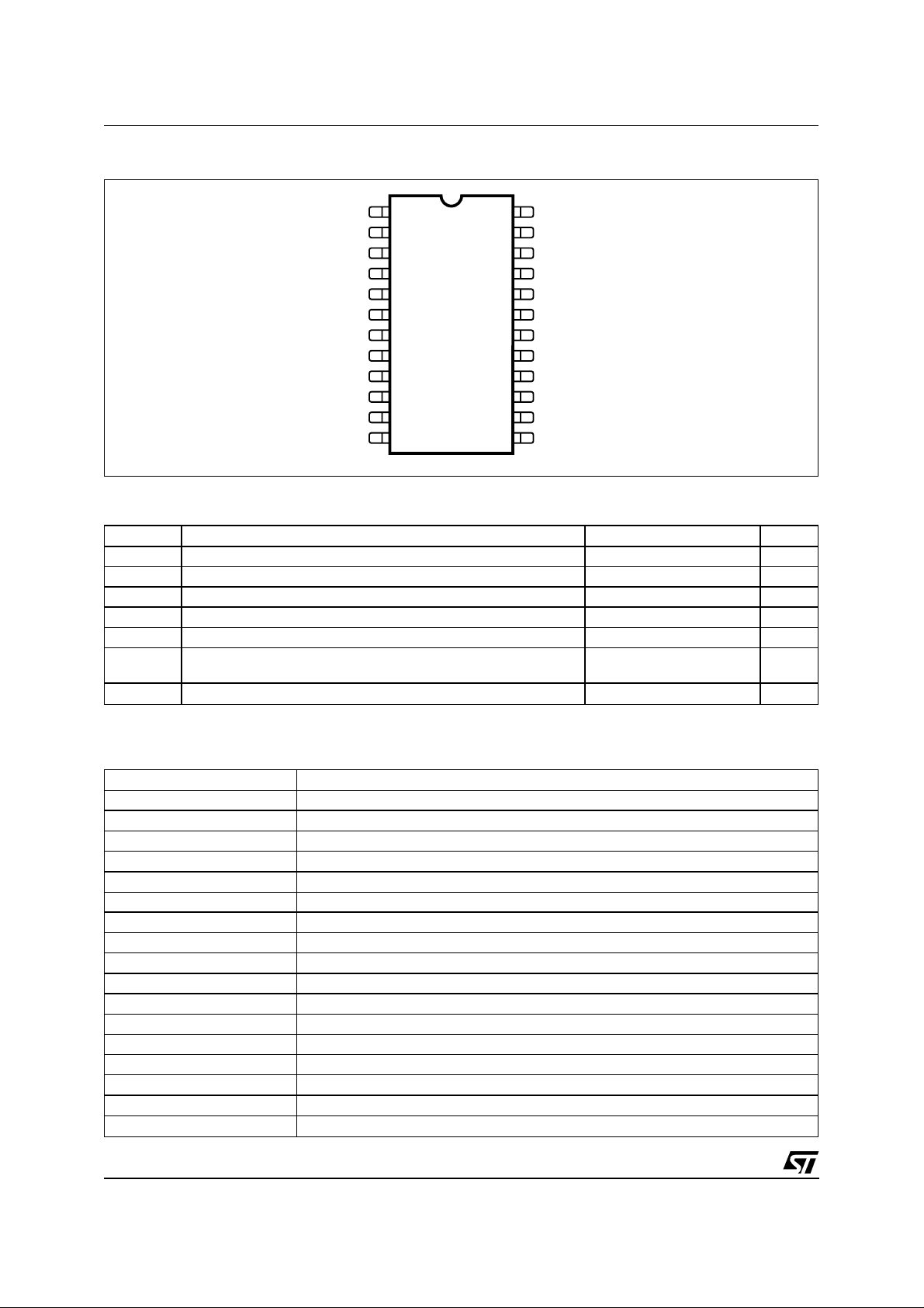
PIN CONNECTION
(Top view)
LOGIC SUPPLY SENSE
VDDA
OUTA
PARK
ENABLE
GND
GND
SENSE IN A
LOGIC SUPPLY FILTER ERROR IN
SENSE IN B VREF
OUT B SENSE OUT11 14
2
3
4
5
6
7
8
9
10
D96IN467
24
23
22
21
20
19
18
17
16
15
1312PARK POWER VDD B
POR DELAY1
VDD SENSE OUT
POWER FAIL THRESHOLD
PARK VOLTAGE PROG
POR
GND
GND
ERROR OUT
ABSOLUTE MAXIMUM RATINGS
Symbol Parameter Value Unit
V
V
V
I
I
P
T
Supply Voltage 14 V
S
Input Voltage 0.3V to V
IN
Differential Input Voltage ±V
ID
DC Output Current 1 A
O
Peak Output Current (non repetitive) 1.2 A
p
tot
Total Power Dissipation (T
Storage and Junction Temperature -55 to +150 °C
stg
= 70°C) 1.2
amb
S
S
W
W
PIN FUNCTIONS
Name Function
V
DD
GND Common Ground.
V
ref
ENABLE Input. Logic low will disable IC.
PARK POWER Input Power supply for the parking circuit.
CURRENT SENSE OUT Current sense operational amplifier output.
ERROR AMP IN Error amplifier inverting input.
ERROR AMP OUT Error amplifier output.
SENSE IN Α/Β Input for external sense resistors.
OUT A, B Outputs of the two Power Operational Amplifiers Connections for Voice coil Motor.
PARK External input for parking. Low will activate the park procedure.
PARK VOLTAGE PROGRAM Input to set the park voltage.
POWER FAIL THRESHOLD Supply monitor threshold setting.
LOGIC SUPPLY SENSE Sense the logic supply level
POR Power on reset output. Low will signal to the controller the failure of the logic supply.
POR DELAY Capacitor connection to set the power on reset delay.
LOGIC SUPPLY FILTER Capacitor connection to filter the logic supply ripple
2/8
Power supply.
Voltage Reference.
L6243DS
THERMAL DATA
Symbol Description Value Unit
R
th j-amb
Thermal Resistance Junction - Ambient 77 to 97 °C/W
ELECTRICAL CHARACTERISTICS
(V
S
= 12V, T
= 25°C; unless otherwise specified)
amb
Symbol Parameter Test Condition Min. Typ. Max. Unit
V
S
I
d
T
j
Supply Range 4.5 13.2 V
Quiescent Drain Current 20 mA
Thermal Shutdown Junction
160 °C
Temperature
ERROR AMPLIFIER
I
b
I
OS
V
OS
Gv Large Signal Open Loop Voltage
GBW Gain Bandwidth 3 MHz
G
min
+ Output Source Current 6 mA
I
O
I
O–-
SR Slew-rate 2 V/µs
Input Bias Current 1 µA
Input Offset Current 300 nA
Input Offset Voltage -5 +5 mV
65 dB
Gain
Minimum Voltage Gain 5
Output Sink Current 6 mA
SENSE AM PL I F IE R
RIN, V
A
d
SR Slew-rate 1 V/µs
GBW Gain Bandwidth Product 3 MHz
R
in
CMRR Common Mode Rejection Ratio 55 dB
V
ref
ref Input Impedance
9KΩ
Differential Gain 8 V/V
Sense Input Impedance 1.5 KΩ
POWER OP. AMP.
G
V
V
d
V
off
Voltage Gain 26 dB
Total Output Voltage Drop IO = 250mA
I
= 500mA
O
I
= 1A
O
Offset Voltage on Sense
450
750
1.15 1.5
mV
mV
V
5mV
Resistor
BW Bandwidth on Resistive Load 100 KHz
3/8

L6243DS
ELECTRICAL CHARACTERISTICS
(continued)
MONITORS AND CONTROL CIRCUIT
Symbol Parameter Test Condition Min. Typ. Max. Unit
V
t2
V
tL
HV
HV
V
ll
I
e
I
p
V
enl
V
enh
V
ph
V
pl
V
pfl
I
prog
I
ch
R
F
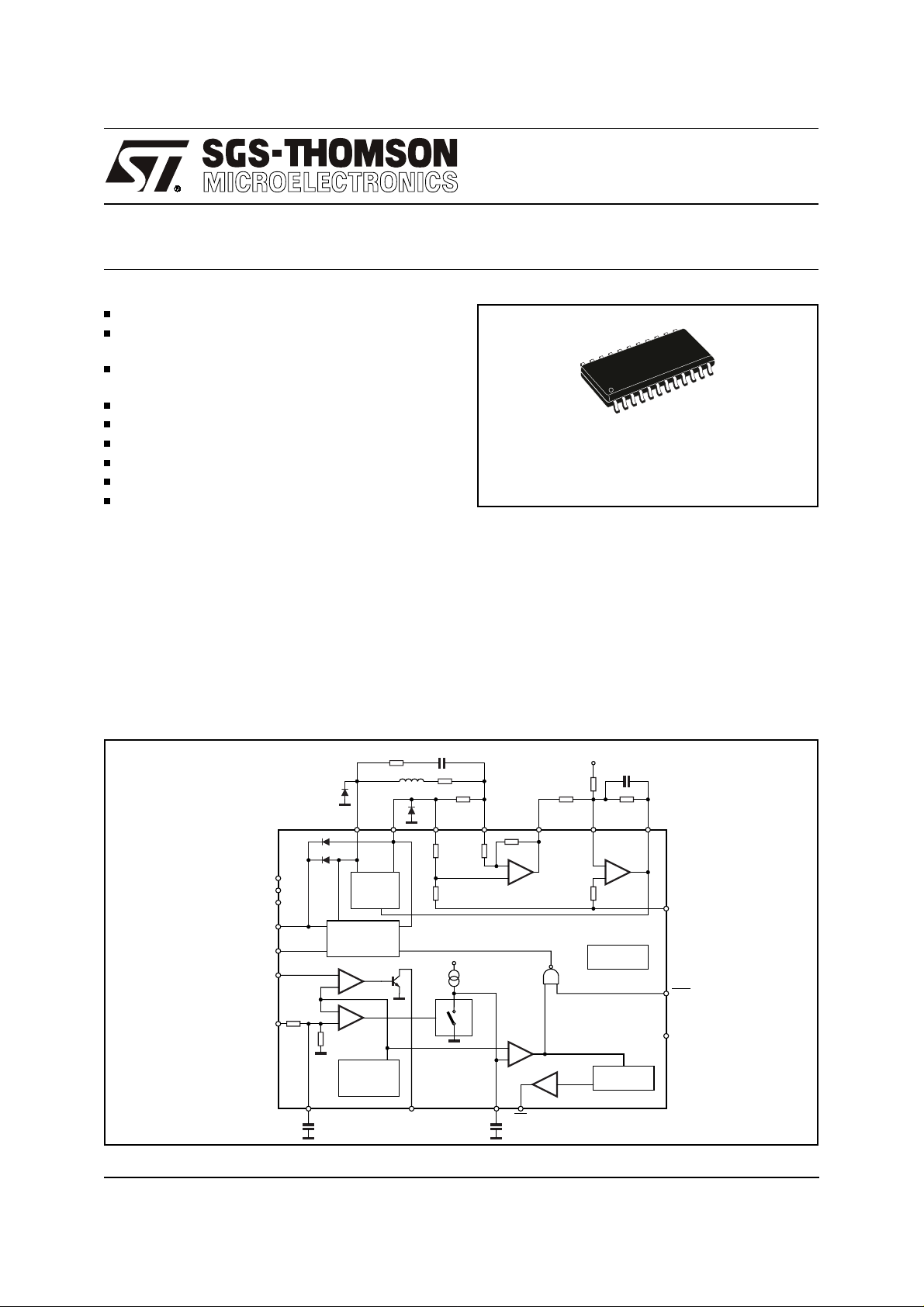
FUNCTIONAL DESCRIPTION
The VCM Driver is controlled via two control signals, ENABLE, POWER ON RESET. An analog
input voltage, ERROR AMP IN, controls the polarity and amplitude of the VCM driving current.
Refer to figure two. This diagram is a representation of the function of the VCM System.
Note that the signals with the bars represent the
"not true", or "non asserted" condit ion. From initial power up, the system is held in the Park
Mode. Upon completion of the POWER UP RESET DELAY the machine moves to Tristate Mode
Threshold Voltage at Logic
Supply Sense
Threshold Voltage at Power Fail
Threshold Input
Hysteresis on Vt2 50 mV
t2
Hysteresis on Vt2 15 mV
tL
Low Level Voltage Power on Reset = 2mA 250 500 mV
Enable Input Current Vi = 2.4V 100 µA
V
= 0.4V –200 µA
i
Input Current at Park Vi = 2.4V 100 µA
V
= 0.4V –200 µA
i
Enable Low Input Voltage 0.8 V
Enable High Input Voltage 2 V
Parking Input High Voltage 2 V
Parking Input Low Voltage 0.8 V
Power Fail Low Output Voltage Il = 2mA 0.5 V
Parking Voltage Program Current 100 µA
Power On Reset Delay
Capacitor Charging
Equivalent Input Resistance at
5V Filter Input
4.2 4.5 V
1.375 1.4 1.435 V
5 µA
6.9 kΩ
BLOCK DESCRIPTION
OUTPUT STAGE
It consists of two Power Op Amps connected in
bridge configuration.
CURRENT SENSE AMPLIFIER
Differential amplifier whose inputs are connected
to the sense lines and whose output is accessible
externally. Closing the loop will transform the
differential voltage signal from the sense lines into
a current signal for the Error Amplifier.
or Run Mode, depending upon the condition of
the ENABLE input. If ENABLE is asserted, the
machine moves directly to Run Mode. If ENABLE
is not asserted, the machine moves to Tristate
Mode.
POWER ON RESET is an asynchronous output.
ERROR AMPLIFIER
Error amplifier which drives the output stage. The
input and the output pins are accessible exter-
nally.
Additionally it affects the internal logic as a hard
wired reset and therefore if a supply failure occurs
during Tristate or Run state, the machine moves
directly back to the Park Mode.
While in Tristate Mode, the assertion of ENABLE
will move the machine to the Run Mode. Run
Mode will typically be the steady running state.
The deassertion of the ENABLE signal causes
the machine to move into Tristate. If it is desired
to perform an active Parking function, the PARK
input must be driven low by the external hardware, or the the VCM can be driven to the Park
position via the ERROR AMP IN control voltage
4/8
POWER SUPPLY MONITOR OPERATION
The circuit monitors the logic supply voltage input
(typ 5V) and activates Power on Reset output
when such a supply drops below the safe operat -
ing limit. After the logic supply voltage reaches its
nominal value a delay capacitor has to be
charged [Tdelay = 3x2x10e5 x C sec] before
Power on Reset output change from low to high
level. Falling edges of Power on Reset are de-
layed (typ 4µs) in order to disable the writing on
the disk before the Power on Reset is activated.
An additional supervisor circuit is present in the

L6243DS
FUNCTIONAL DESCRIPTION
Function Description
input This is the Power Supply input.
V
DD
POWER FAIL
THRESH
V
SENSE OUT
CC
Output
LOGIC SUPPLY
SENSE input
PARK POWER
input
PROGRAMMABLE
PARK VOLTAGE
input
PARK input Logic signal asserted low, activates parking.
POWER ON RE-
SET output
POWER ON RE-
SET DELAY in-
put
ENABLE input This signal originates at the external controller and, when asserted, allows the VCM Drivers to
input The reference voltage input is basically that voltage, at which the output current is zero.
V
REF
ERROR AMP IN
input
ERROR AMP OUT
output
OUTPUT A power
output
OUTPUT B power
output
SENSE AMP IN
A/B signal input
SENSE AMP OUT
signal output
LOGIC SUPPLY
FILTER
Input for the V
TTL compatible signal indicating the VCC supply has dropped below the POWER FAIL
THRESHOLD.
This pin allows the monitoring of 5V supply. When a low voltage is detected POR is asserted
This input is used during the Power Down/Power Fail Parking operation. When the supply goes
down, a typical Spindle Driver Circuit automatically tristates its output stages. During this time
the spindle motor spins freely and the stored energy is used to drive the VCM to the park
position. The generated BEMF is rectified and filtered across an external PARKING
CAPACITOR.
Used to set the voltage applied to the VCM during an Automatic Parking Operation.
Indicates an error condition to the external control and support circuitry. A Logic Supply Fail
condition automatically initiates a POWER ON RESET. Internal 30k Pullup to LSS.
The intent of this input is to provide a time delay at power up. During this time, the POWER ON
RESET line will be asserted (low). A POWER ON RESET, will hold the system in the PARK
mode. Once the delay has timed out, the POWER ON RESET will be removed to allow the
external system to assume control. When applied in a Disk Drive Application, the POWER ON
RESET DELAY will be required to have a minimum duration which will ensure that the
Read/Write Heads can be fully parked.
operate. When deasserted the VCM Driver is forced into Tristate mode. During a POWER ON
RESET condition however, the parking operation is automatic and takes priority over the
ENABLE function. Only at the end of the POWER ON RESET DELAY will the ENABLE input
become active. If active parking is desired, it will be accomplished under control of the V
signal, otherwise it is an automatic function at power down.
Inverting input of error amplifier. The non inverting one is internally tied to V
Error amplifier output pin. Open collector output.
Voice Coil power output.
Voice Coil power output.
Sense amplifier input pins. The sense resistor is connected across these pins.
Output pin of sense amplifier.
Capacitor connection to avoid false triggering
IC with a programmable threshold, which is set
by an external resistive divider. The TTL compatible output can be us ed separately or connected
to Park input in order to park the head.
(continued)
supply monitor. The Threshold can be externally set via a voltage divider.
CC
.
ref
voltage is set by connecting an external resistor
between Park Voltage Program input and
ground: (Vpark=Rext x Iref, Iref=100µA typ). Con-
necting ENABLE input to GND the driver will be
disabled (outputs in high impedance mode).
IN
PARKING CIRCUIT OPERATIONT
The voice coil driver is switched into the parking
condition when Power on Reset output or Park input are low. In such a condition a fixed voltage is
superimposed on the load and the value of such a
THERMAL SHUTDOWN
It will disable the IC when the junction tempera-
ture exceeds the threshold value above which the
device could be damaged.
5/8

L6243DS
Figure 1:
Application Circuit
(*)
VCM
0.1µF
100
(*) VALUES TO BE SET IN APPLICATION
5V
0.5
1
24
6,7,18,19
3
11
8
10
9
(*)
21
22
17
16
14
(*)
1.8nF
D96IN468
V
DD
13K
2K
V
IN
1.5K5K
1.5K
Figure 2:
Application Circuit
LOGIC SUPPLY SENSE
POWER ON DELAY INPUT
POWER ON RESET
d
POWER ON RESET DELAYt
D96IN470
6/8

SO24 PACKAGE MECHANICAL DATA
L6243DS
DIM.
MIN. TYP. MAX. MIN. TYP. MAX.
A 2.35 2.65 0.093 0.104
A1 0.10 0.30 0.004 0.012
A2 2.55 0.100
B 0.33 0.51 0.013 0.0200
C 0.23 0.32 0.009 0.013
D 15.20 15.60 0.598 0.614
E 7.40 7.60 0.291 0.299
e 1.27 0,050
H 10.0 10.65 0.394 0.419
h 0.25 0.75 0.010 0.030
k0° (min.), 8° (max.)
L 0.40 1.27 0.016 0.050
mm inch
A2
A
0.10mm
.004
Seating Plane
Be
A1
K
D
1324
E
112
h x 45?
L
A1 C
H
SO24
7/8

L6243DS
Information furnis hed is believe d to be ac curate and reliabl e. However, SGS-THOMS ON Mi croelectroni cs as sumes no res ponsib ility for the
consequences of use of such inf orm ation nor for any i nfringem ent of patents or othe r ri ghts of third parties whi ch m ay result from its use. No
license is granted by implication or otherwise under any patent or patent rights of SGS-THOMSON Microelectronics. Specification mentioned
in this p ublication are subject to c hange w ithout not ice. T his pub lic ation super sedes a nd replaces all informa tion previous ly supplied. SGSTHOMSON Mic roelectronics products are not author ized for use as cri tical components in l ife support devices or systems with out express
written approval of SGS-THOMSON Microelectronics.
© 1998 SGS-THOMSON Microelectronics – Printed in Italy – All Rights Reserved
SGS-THOMSON Microelectronics GROUP OF COMPANIES
Australia - Brazil - Canada - China - France - Germany - Italy - Japan - Korea - Malaysia - Malta - Morocco - The Netherlands -
Singapore - Spain - Sweden - Switzerland - Taiwan - Thailand - United Kingdom - U.S.A.
8/8
 Loading...