

OUTPUTCURRENT UP TO 1A
OPERATESAT LOW VOLTAGESWITH LOW
COILRESISTANCEOF THE MOTOR
LARGE COMMON MODE AND DIFFEREN-
TIALMODERANGE
LOW INPUT OFFSETVOLTAGE
THERMAL SHUT-DOWN
ENABLEFUNCTION
INTERNAL CLAMP DIODES
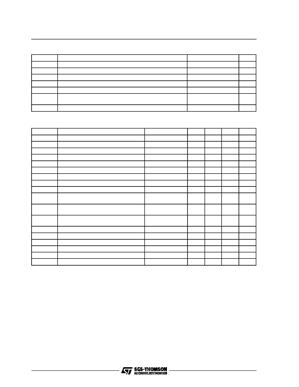
L6242
VOICE COIL MOTORDRIVER
ADVANCE DATA
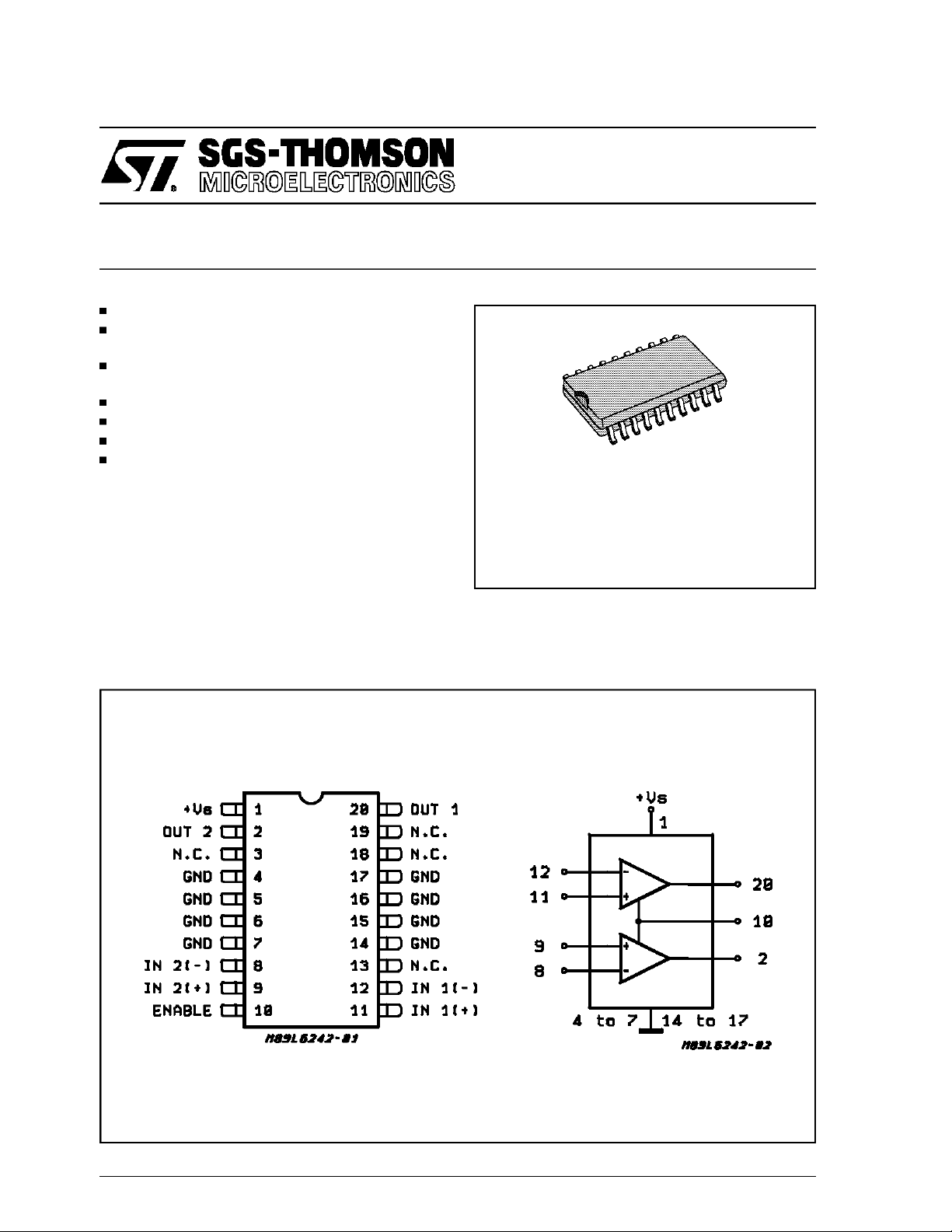
SO20
DESCRIPTION
TheL6242is a monolithicintegratedcircuit in SO-20
package intended for use as a dual power operational amplifier. It is particularly indicated for driving inductive loads as linear motor, and finds applicationin Hard Disc, Compact-Disc, etc.
The two power operational amplifiers are controlled by a common enable input.
PIN CONNECTION AND BLOCK DIAGRAM
ORDERINGNUMBER: L6242
Thehigh gain and output power capabilityprovide
superior performance whatever a power booster
isrequired.
November 1991
This is advanced information on a new product now in development or undergoing evaluation. Details are subject to changewithoutnotice.
T is advanced informationon a new product now in development or undergoingevaluation. Details are subject to change without
1/5
L6242
ABSOLUTE MAXIMUM RATINGS
Symbol Parameter Value Unit
V
V
V
I
I
P
T
stg,TJ
ELECTRICAL CHARACTERISTICS (VS= 12V, TJ=25°C unlessotherwisespecified)
Symbol Parameter Test Condition Min. Typ. Max. Unit
V
I
I
V
I
OS
S
R
G
CMR Common Mode Rejection f = 100Hz 66 84 dB
SVR Supply Voltage Rejection f = 100Hz R
V
drop
V
drop
T
R
V
I
eq
T
I
Supply Voltage 28 V
S
Input Voltage VS V
i
Differential Input Voltage ±V
i
DC Output Current 1 A
O
Peak Output Current (non repetitive) 1.5 A
P
Maximum Power Dissipation at T
tot
amb
T
CASE
=85°C
=75°C
S
1
5
Storage and Junction Temperature Range -40 to 150 °C
Supply Voltage 4 28 V
S
Quiescent Drain Current VO=VS/2 10 15 mA
S
Input Bias Current 0.2 1 µA
b
Input Offset Voltage 15 mV
OS
Input Offset Current 10 50 nA
Slew Rate 1.5 V/µs
r
Input Resistance 500 KΩ
i
Open Loop Voltage Gain f = 100Hz 70 80 dB
V
= 10KΩ
V
r
= 0.5V
g
High Drop Voltage I = 100mA
I = 500mA
Low Drop Voltage I = 100mA
I = 500mA
Thermal Shutdown Junction Temperature 145 °C
sd
Internal Pull-up Resistor of the Enable Input 50 KΩ
p
Enable Low Voltage TJ= 130°C -0.3 1.2 V
e
54 dB
0.7
1 1.5
0.3
0.6 1
Quiescent Drain Current En = L 2 5 mA
Enable Delay 50 µs
d
Output LeakageCurrent 10 µA
ol
V
W
W
V
V
V
V
APPLICATION INFORMATIONS
Figure 1 shows the L6242 configurated as a transconductance amplifier, in order to drive linear
motors as VoiceCoil (VCM). The L6242 provides
the power section of the Transconductance Amplifier. The two OP AMP are configurated one as
inverting and the other as noninvertingamplifier,
with the same gain. Working in push-pull, they
can be configurated as a bridge. The motor current can be controlled by means of the sense resistor (typical 1Ω) in series with the motor. The
currentsense amplifier provides the feedback signal, which is summed to the driving signal at the
node which is the inverting input of the Error Am-
2/5
plifier. R1 closes the control loop. R2 converts the
input voltage signal, into a current signal.
The snubber network provides the system stability, always required by the application. The network is directly connected to the output pins of
the IC, OUT1 and OUT2, and in parallel with the
load. R4 and C2 could be of different values, depending on the p.c.b. configuration and on the
motorcharacteristics.
TheDC transferfunctionmay be expressedas:
gm = Iout/Vin = k • (R1/R2)
wherek = 1/(Rsense •Ad)
and Ad = gain of thecurrent senseamplifier.

Figure1: Voice Coil Motor Control Circuit
L6242
OPTIMIZINGLAYOUT
Optimizing a PC board layout involves to observe
the following rules which in general can avoid application problems associated with ground loops
and anomalous recirculation currents. The electrolytic capacitor for the power supply must be
kept as close to the IC as possible. It is important
that power grounds are close to each other on a
wide enough. Copper side also, it is important to
separate on the board the logic ground and the
power ground in such a way that the ground
traces for the logic signals and references do not
cross the ground traces for the power signals.
Logic ground and power ground must meet at
one point on the board (startpoint grounding) far
enough away from where the power ground
traces terminate to ground (sense resistors and
recirculation diodes). This is to avoid anomalous
interface with the logic signals. It is generally a
good idea to connect a non inductive capacitor
(typically 100nF) between the pins VS and GND.
In other cases it may be necessary to also place
a by-pass capacitor between the pins Vref and
GND.
3/5

L6242
SO20PACKAGE MECHANICAL DATA
DIM.
MIN. TYP. MAX. MIN. TYP. MAX.
A 2.65 0.104
a1 0.1 0.3 0.004 0.012
a2 2.45 0.096
b 0.35 0.49 0.014 0.019
b1 0.23 0.32 0.009 0.013
C 0.5 0.020
c1 45 (typ.)
D 12.6 13.0 0.496 0.512
E 10 10.65 0.394 0.419
e 1.27 0.050
e3 11.43 0.450
F 7.4 7.6 0.291 0.299
L 0.5 1.27 0.020 0.050
M 0.75 0.030
S 8 (max.)
mm inch
4/5

L6242
Information furnished is believed to be accurate and reliable. However, SGS-THOMSON Microelectronics assumes no responsibility for the
consequences of use of such information nor for any infringement ofpatents or otherrights of thirdparties which may resultfrom its use. No
license isgranted by implication or otherwise under any patent or patent rights of SGS-THOMSON Microelectronics. Specifications mentioned in this publication are subject to change without notice. This publication supersedes and replaces all informationpreviously supplied.
SGS-THOMSON Microelectronics products are not authorized for use as critical components in life support devices or systems without express writtenapproval of SGS-THOMSON Microelectronics.
1994 SGS-THOMSON Microelectronics - All RightsReserved
SGS-THOMSON Microelectronics GROUP OF COMPANIES
Australia - Brazil - France - Germany - Hong Kong - Italy - Japan - Korea - Malaysia -Malta - Morocco - The Netherlands - Singapore -
Spain - Sweden - Switzerland - Taiwan - Thaliand - United Kingdom - U.S.A.
5/5
 Loading...