

12V SENSORLESS SPINDLE MOTOR CONTROLLER
12V OPERATION
3A,THREE-PHASEDMOS OUTPUT
(TOTALR
NOHALLSENSORSREQUIRED
DIGITALBEMFPROCESSING
LINEAROR PWM CONTROL
STANDALONE OR EXT. DRIVER
SHOOT-THROUGHPROTECTION
THERMALSHUTDOWN
dson
0.52Ω)
L6238S
PRODUCT PREVIEW
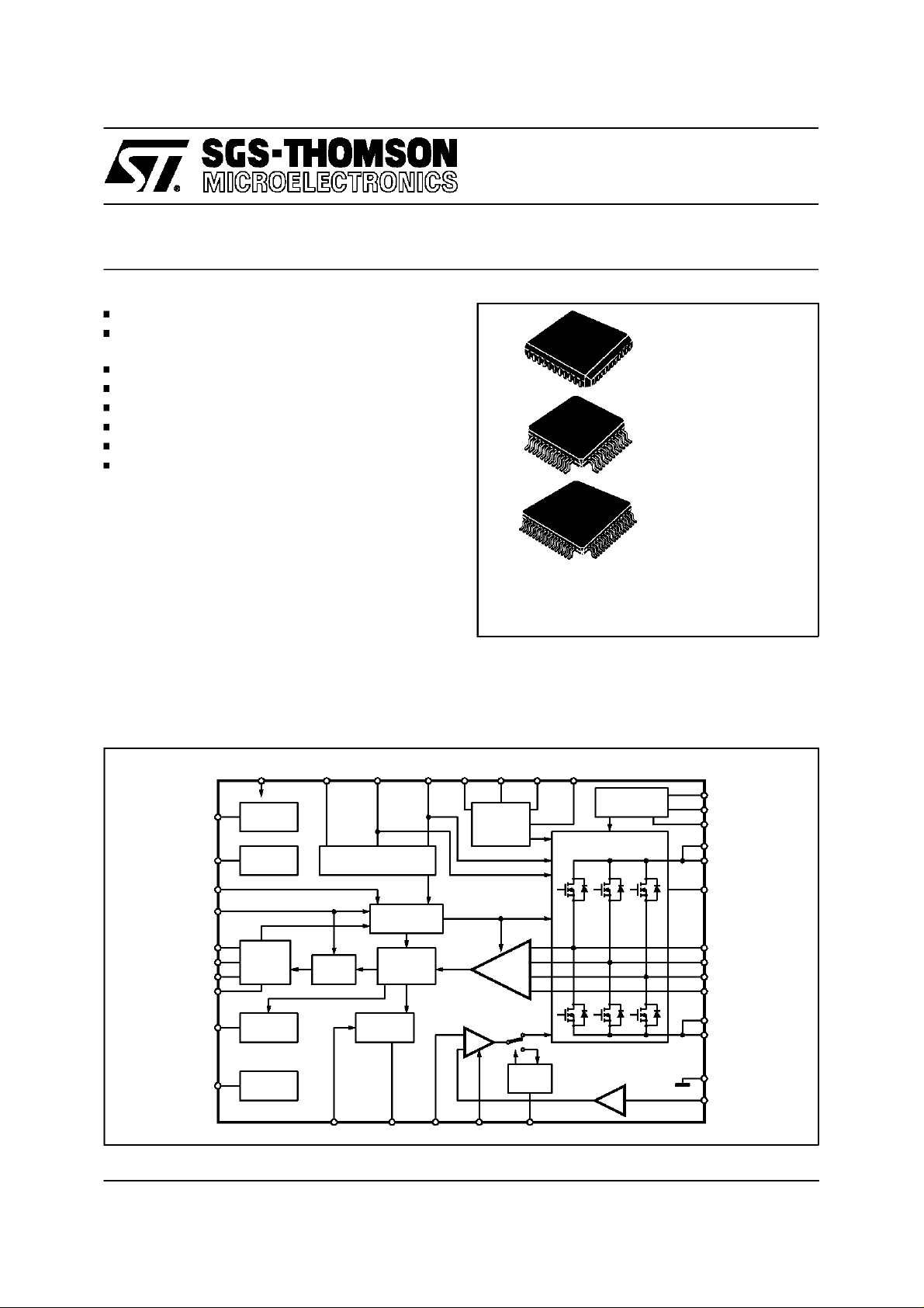
PLCC44
PQFP44
DESCRIPTION
The L6238S is a Three-Phase, D.C. Brushless
Spindle MotorDriver system. This device features
boththe Powerand SequenceSections.
Higher Power Applications can be activied with
the additionof an external Linear Driver,or by operatingthe InternalDrivers in PWM.
Motor Start-Up, without the use of Hall Sensors,
can be achieved either by an internal start-up algorithm or by manually sequencing the Output
Drivers, using a variety of User-Defined Start-UP
Algorithms.
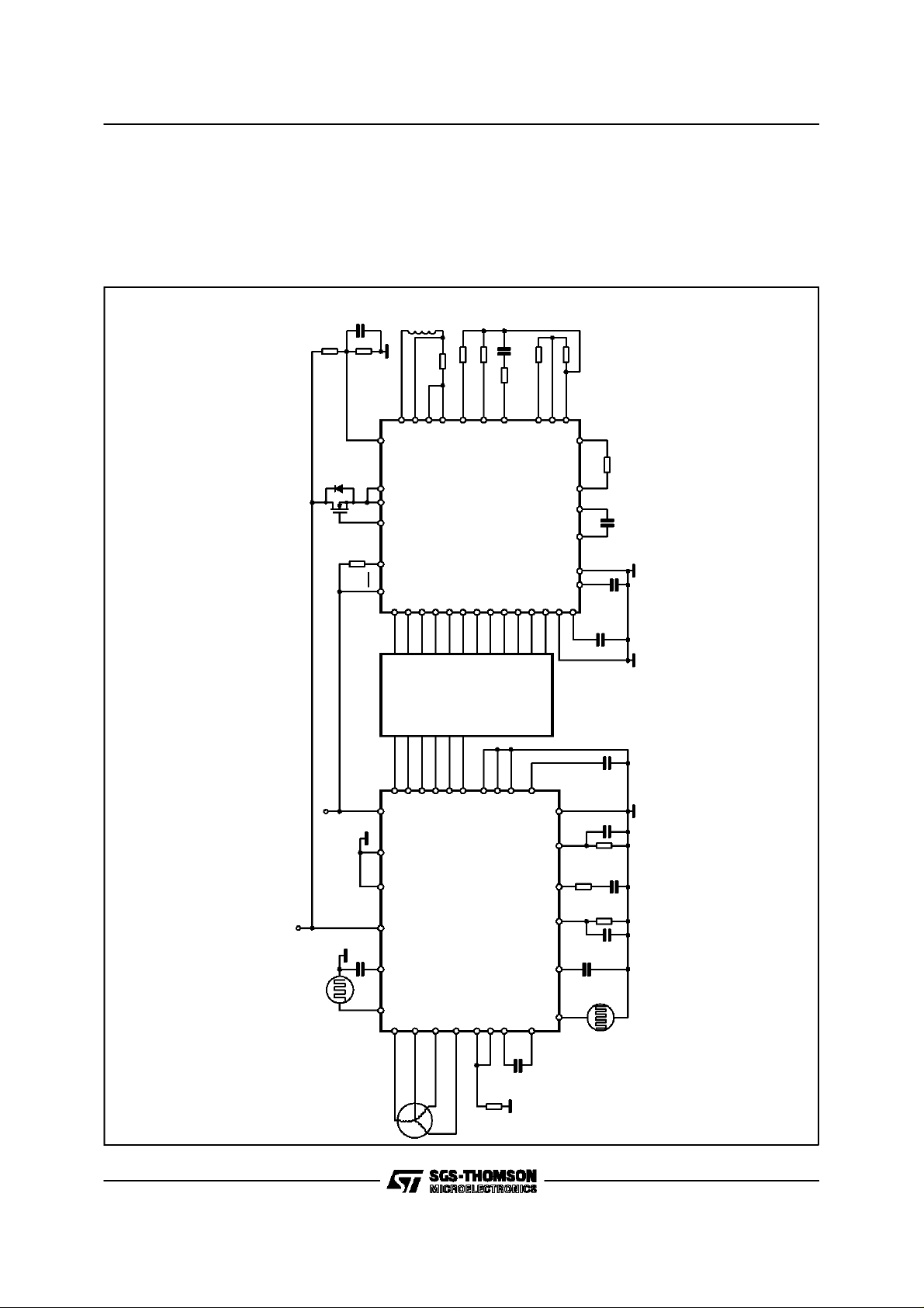
BLOCKDIAGRAM
VANALOG
SYS CLOCK
SEQ INCR
MONO/SEQ
CTRL
TDLY(0)
TDLY(1)
TDLY(2)
MASK DLY
VL
BIAS
SYSTEM
CLOCK
DIGITAL
DELAY
FALIGN
MONO
DET
OUTPUT
ENABLE
ALIGN + GO
START-UP
RUN/
BRAKE
SEQUENCER
ZERO
CROSSING
DETECTOR
TQFP64
ORDERING NUMBERS: L6238S (PLCC44)
L6238SQA (PQFP44)
L6238SQT (TQFP64)
Protection features include Stuck Rotor\Backward
Rotation Detection and Automatic Thermal Shutdown.
PWM
PWM
LIN
BEMF
SENSE
PWM
COMP
+
+
+
-
TIM
CHARGE
POWER
STAGE
PUMP
CPUMP1
CPUMP2
CPUMP3
VPOWER
BRAKE
DELAY
OUT A
OUT B
OUT C
CTR TAP
PWM/
SLEW
ONE-SHOT
SLEW-CTRL
RSENSE1
RSENSE2
GND
CSA INPUT
1/31
OT-WARN
October 1995
SPIN
SENSE
TOGGLE
THERMAL
SHUTDOWM
DIVIDE
BY N
FMTRSEL POL
VCTRL
+
-
DRV
CNTL
GATE DRIVEGM COMP
AV=4V/V
CSA
D95IN232
This isadvanced information on a new product now in development or undergoing evaluation. Details are subject to changewithout notice.
L6238S
ABSOLUTE MAXIMUM RATINGS
Symbol Parameter Value Unit
BV
dss
V
Power
V
Logic
V
Analog
V
in
C
storage
I
mdc
I
mpk
P
tot
Ts Storage and Junction Temperature -40 to 150 °C
THERMALDATA
Symbol Parameter PLCC44 PQFP44 TQFP64 Unit
R
th (j-amb)
Those Thermal Data arevalid if the package is mounted on Mlayer board in stillair
Output Brakdown Voltage 17 V
Motor Supply Voltage 15 V
Logic Supply Voltage 7 V
Analog Supply Voltage 15 V
Input Voltage -0.3 to 7 V
Charge Pump Storage Capacitor 4.7 µF
Motor Current (DC) (TQFP64 only)
(PLCC44 and PQFP44)
3
2.5
Peak Motor Current (Pulsed: Ton= 5ms, d.c. = 10%) 5 A
Power Dissipation at Tamb = 50 °C(PLCC44)
(TQFP64)
(PQFP44)
2.3
1.7
1.3
Thermal Resistance Junction-Ambient 34 45 45 °C/W
A
A
W
W
W
PIN CONNECTION PLCC44 (Topview)
7
GND
N.C.
GND
8
9
10
11
12
13
14
15
16
17
CHARGE PUMP 1
CHARGE PUMP 3
OUTPUT A
VPOWER
VANALOG
TDLY(0)
TDLY(1)
TDLY(2)
CHARGE PUMP 2
GND
OTWARN
SELECT POLE
BRAKE DELAY
RSENSE 1
PWM/LINEAR
PWM LIMIT TMR
OUTPUT B
SPIN SENSE
123564
2322211918 20 28272624 25
RUN/BRAKE
OUTPUT ENABLE
VPOWER
PWM/SLEW
CENTER TAP
SYSTEM CLOCK
SEQ. INCREMENT
MONO/SEQINC CTRL
GND
MASK DELAY
40414244 43
FALIGN
PWM COMP
39
38
37
36
35
34
33
32
31
30
29
GND
GATE DRIVE
GM COMP
OUTPUT C
RSENSE 2
CSA INPUT
VCONTROL
N.C.
FMOTOR
VLOGIC
GND
D95IN245
2/31
PIN CONNECTION PQFP44 (10x10)(Top view)
TDLY(2)
GND
TDLY(1)
OTWARN
SELECT POLE
PWM LIMIT TIMER
PWM/LINEAR
OUTPUT ENABLE
RUN/BRAKE
SEQ. INCREMENT
SYSTEM CLOCK
MONO/SEQINC CTRL
FALING
PWM COMP.
12
13
14
15
16
18
19
20
21
22
GND
VLOGIC
FMOTOR
N.C.
TDLY(0)
N.C.
VCONTROL
VANALOG
VPOWER
2827262423 25 33323129 30
RSENSE 2
CSA INPUT
OUTPUT A
OUTPUT C
CHARGE PUMP 1
CHARGE PUMP 3
GM COMP
GATE DRIVE
GND
123564789101711
44
43
42
41
40
39
38
37
36
35
34
GND
L6238S
GND
CHARGE PUMP2
RSENSE 1
BRAKE DELAY
SPIN SENSE
OUTPUT B
PWM/SLEW
CENTER TAP
VPOWER
MASK/DELAY
GND
D95IN243
PIN CONNECTION TQFP64 (Topview)
GND
GND
17
N.C.
18
N.C.
N.C.
GND
19
20
21
22
23
25
26
27
28
29
30
31
32
GND
OTWARN
SELECT POLE
PWM LIMIT TMR
PWM/LINEAR
OUTPUT ENABLE
RUN/BRAKE
SEQ. INCREMENT
SYSTEM CLOCK
MONO/SEQINC CTRL
FALIGN
PWM COMP
GND
GND
TDLY(1)
TDLY(2)
VLOGIC
FMOTOR
VANALOG
TDLY(0)
1213141516
37363433 35
CSA INPUT
VCONTROL
VPOWER
VPOWER
RSENSE 2
RSENSE 2
N.C.
N.C.
OUTPUT A
OUTPUT A
4342413938 40 48474644 45
OUTPUT C
OUTPUT C
CHARGE PUMP 3
GM COMP
CHARGE PUMP 1
GATE DRIVE
GND
GND
GND
GND
GND
123564789102411
64
63
62
61
60
59
58
57
56
55
54
53
52
51
50
49
GND
GND
GND
CHARGE PUMP 2
RSENSE 1
RSENSE 1
BRAKE DELAY
SPIN SENSE
OUTPUT B
OUTPUT B
PWM/SLEW
CENTER TAP
VPOWER
VPOWER
MASK DELAY
GND
GND
D95IN244
3/31

L6238S
PIN FUNCTIONS
PLCC44 PQFP44 TQFP64 Name I/O Function
1 39 56, 57 OUTPUT B I/O DMOS Half Bridge Output and Input B for Bemf sensing.
2 40 58 SPIN SENSE O Toggless at each Zero Crossing of the Bemf.
3 41 59 BRAKE DELAY I Energy Recovery time constant, definedby external R-C to ground.
4 42 60, 61 R
sense 1
5 43 62 CHARGE
PUMP 2
6, 7,
17, 29,
39, 40
1, 11,
23, 33,
34, 44
* GROUND S Ground terminals.
8 2 4 CHARGEPUMP1 I Positive terminal of Pump Capacitor.
9 3 5 CHARGEPUMP3 O Positive terminal of Storage Capacitor.
10 4 6, 7 OUTPUT A I/O DMOS Half BridgeOutput and Input A for Bemf sensing.
11, 42 5, 36 9, 10,
V
power
52, 53
12 6 11 V
13, 32 7, 26 8, 18,
analog
N.C N.C Open Terminal
19, 31,
41
14 8 12 Tdly(0) I Three bits that set theDelay between the detection of the Bemf
15 9 13 Tdly(1) I
16 10 14 Tdly(2) I
18 12 20 OTWARN O Overtemperature Warning Output
19 13 21 SELECT POLE I Selects # of Motor Poles. A zero selects 8, while a one selects 4
20 14 22 PWM TIMER I Capacitor connected to this pin sets the maximum time allowed
21 15 23 PWM/LINEAR I Selects PWM or Linear Output Current Control
22 16 24 OUTPUT
ENABLE
23 17 25 SEQUENCE I Rising edge will initiate start-up. A Brakingrountine is started
24 18 26 SEQ
INCREMENT
25 19 27 SYSTEM CLK I Clock Frequency for the system timer/counters.
26 20 28 MONO/SEQ.
INC. CONTROL
27 21 29 Falign I Reference Frequency for the opt. Auto-Start Algorithm. If int.
28 22 30 PWM COMP O Output of the PWM Comparator
30 24 35 Vlogic S 5V Logic Supply Voltage.
31 25 36 Fmotor O Motor Once-per-Revolution signal.
33 27 37 Vcontrol I Voltage at this input controlshe Motor Current
34 28 38 CSA INPUT I Input to the Current Sense Amplifier.
35 29 39, 40 Rsense 2 O Output C connection forthe Motor Current SenseResistor to
36 30 42, 43 OUTPUT C I/O DMOS Half Bridge Output and Input C for Bemf sensing.
37 31 44 gm COMP I A series RC network to ground that defines the compensation of
O Outputs A+B connections for the Motor Current Sense Resistor
to ground
I Negative Terminal of Pump Capacitor.
S Power Section Supply Terminal.
S 12V supply.
zero crossing, and the commutation of the next Phase.
poles.
for 100% duty cycle during PWM operation
I Tristates Power Output Stage when a logic zero.
when this input is brought low.
I A lowto high transition on thispin increments the Output State
Sequencer.
I A logicone will disable the Monotonicity Detectorand Sequence
Increment functions.
start up is not used, this pin must be connected to the System
Clock.
ground.
the Transconductance Loop.
4/31
PIN FUNCTIONS
PLCC44 PQFP44 TQFP64 Name I/O Function
38 32 45 GATE DRIVER I/O Drivers the Ext. PFET Gate Driver for Higher Power applications.
This pin must be grounded if anexternal driver is not used.
41 35 51 MASK/DELAY O Internal Logic Signals used forproduction Testing
43 37 54 CENTER TAP I Motor Center Tap used for differentialBEMF sensing.
44 38 55 PWM/SLEW I R/C at this input set the LinearSlew Rate and PWM OFF-Time
L6238S
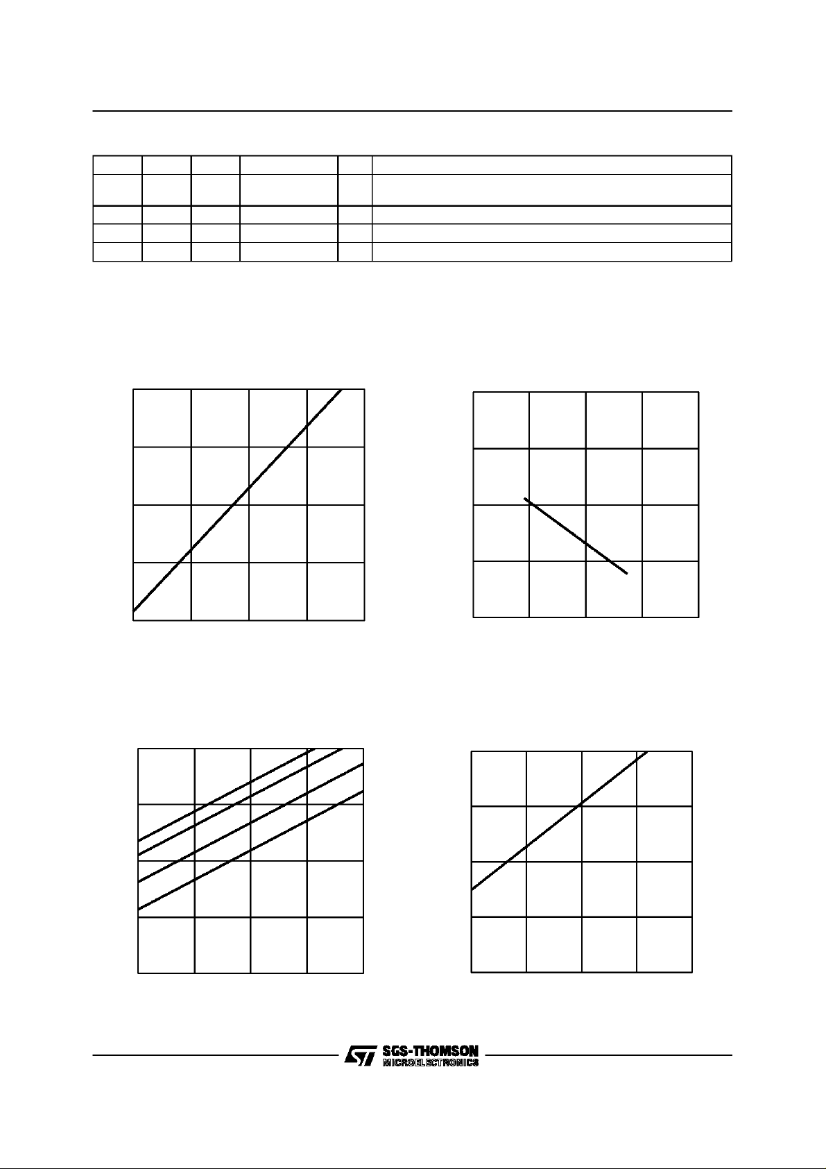
Figure1: BrakeDelay TimeoutvsC
(R
T
BD
(s)
3.0
1.0
0.3
0.0
0.0 0.3 1.0 3.0 Cb(µF)
Figure3: PWM Off - Time vs R
brake
=1Meg)
slew/Coff
brake
D95IN274
Figure 2: LinearSlew Rate vs R
S
VR
slew
(V/µs)
3.0
1.0
0.3
0.0
10 30 100 300 Rs(KΩ)
Figure 4: PWMLimit Time - Out vsC
D95IN275
timer
PWM
(µs)
D95IN276
30
10
3
1
100 300 Coff(pF)
PWM
(µs)
30
10
100 300 Ctimer(pF)
D95IN277
5/31
L6238S
ELECTRICAL CHARACTERISTICS (T
=0to70°C; VA=V
amb
Pwr
= 12V; V
= 5V; unless otherwise
logic
specified)
Symbol Parameter Test Condition Min. Typ. Max. Unit
GENERAL
V
analog
I
analog
V
I
logic
logic
Analog Supply Voltage 10.5 13.5 V
Analog Supply Current Run Mode VA= 13.5V 1.5 2.7 4.5 mA
Brake Mode V
= 13.5V 280 800 µA
A
Logic Supply Voltage 4.5 5.0 5.5 V
Logic Supply Current Run Mode V
= 5.5V 1 2 3.2 mA
logic
Brake Mode 100 500 1000 µA
THERMAL SHUTDOWN
*T
*T
*T
sd
hys
ew
Shut Down Temperature 150 180 °C
Recovery Temperature
30 °C
Hysteresis
Early Warning Temperature Tsd-25 °C
POWERSTAGE
R
DS(on)
I
o(leak)
V
F
dVo/dt Output Slew Rate (Linear) R
I
gt
V
Gate-Drive
V
Ctrl-Range
I
in(VCtrl)
PWM OFF-TIME CONTROLLER (R
T
off
V
chrg
V
trip
Output ON Resistance per FET Tj=25°C; VA= 10.5V
T
= 125°C; VA= 10.5V
j
Output Leakage Current V
= 15V 1 mA
pwr
0.20 0.26
0.40
Body Diode Forward Drop Im= 2.0A 1.5 V
= 100KΩ 0.15 0.30 0.45 V/µs
slew
Output Slew Rate (PWM) 10 150 V/µs
Gate Drive for Ext. Power
DMOS
V
V
control
A
= 1V; V
= 10.5V
sns
= 0V;
4.5 mA
Ext Driver Disable Voltage 0.7 V
Voltage Control Input Range 0 5.0 V
Voltage Control Input Current 10 µA
= 100KΩ,C
slew
= 120pF)
off
OFF Time 9 11 14 µs
Capacitor Charge Voltage VA= 10.5V 2.31 2.65 3.1 V
Lower Trip Threshold 1.25 V
Ω
Ω
PWM LIMITTIMER
I
chrg
V
chrg
V
trip
Capacitor Charge Current V
PWM Timer
= 0V; VA= 10.5V 10.0 20.0 30 µA
Capacitor Charge Voltage VA= 10.5V 3.0 3.5 4.0 mV
Lower Trip Threshold 100 400 V
BEMF AMPLIFIER
V
Z
inCT
Bemf
Center Tap Imput Impedance 20 30 40 KΩ
Minimum Bemf (Pk-Pk) 60 mV
CURRENT SENSE AMPLIFIER
I
snsin
G
v
SR Slew Rate 0.33 0.8 V/µs
6/31
Input Bias Current VA= 13.5V 10 µA
Voltage Gain 3.8 4.0 4.2 V/V
ELECTRICALCHARACTERISTICS (Continued)
Symbol Parameter Test Condition Min. Typ. Max. Unit
BRAKEDELAY
V
V
chrg
I
in
I
out3
Thres
Capacitor Charge Voltage RT= 50K 8.8 9.6 10.5 V
Input Current Vin= 5.0V 500 nA
Source Current VA= 10.5V 0.5 mA
Delay Timer Low TripThreshold 1.2 1.8 2.8 V
CHARGEPUMP
V
out
F
cp
I
in
I
brkdly
I
brake
Storage Capacitor Output
VA= 10.5V; I
= 500µA17 V
out
Voltage
Charge Pump Frequency 140 450 KHz
Vstorage Input Current (Run
V
storage
= 12V; VA=V
=0 25 µA
logic
Mode)
Vstorage Leakage Current
V
storage
= 12V; VA=V
= 0 0.4 1 µA
logic
(Brake Delay Mode)
Vstorage Leakage Current
V
storage
= 12V; VA=V
= 0 0.1 1 µA
logic
(Brake Mode)
SEQUENCEINCREMENT
t
seq
Time Between Rising Edges 1 µs
OUTPUT TRANSCONDUCTANCE AMPLIFIER Note:Measure at OTA Comp. pin.
V
V
outL
I
source
I
sink
oh
Voltage Output High VA= 10.5V 10 V
Output Voltage 2.0 V
Output Voltage 40.0 0.5 V
Output Sink Current 40.0 µA
L6238S
LOGICSECTION
V
inH
V
inL
V
inH
V
inL
I
inH
I
inL
V
outL
V
inL
F
sys
t
off/ton
Input Voltage (All Inputs
V
Except Run/Brake
Run/Brake Input Voltage V
Input Current
Output Voltage Vsink = 2.0mA
V
System Clock Frequency 8.0 12.0 MHz
Clock ON/OFF Time 20 ns
Phase DelayTruth Table
Tdelay (2) Tdelay (1) Tdelay (0)
1 0 1 2.0
1 0 0 9.4
1 1 1 18.80
1 1 0 20.68
0 0 1 22.56
0 0 0 24,44 (*)
0 1 1 26.32
0 1 0 28.20
(*) Input Default
= 4.5 to 5.5V 3.5
logic
= 4.5 to 5.5V 2.0
logic
= 2.0mA 4.5
source
1.5
1.0
1.0 µA
-1.0
0.5 V
Commutation Phase Delay,
in Electrical Degrees
V
V
V
V
mA
V
7/31
L6238S
FUNCTIONAL DESCRIPTION
1.0 INTRODUCTION
1.1 Typical Application
In a typical application,the L6238Swill operatein
conjunction with the L6244 Voice Coil Driver as
Figure1-1
27K
10K
0.1µF
3.6K
SENSE
V
Vpower
GATE
POR
V
VCM
SENSE +INPUT
SENSE -INPUT
OUT A
CC
458
38
42
44 9 37
DRIVE
43 35
19
LOGIC
data(0)20data(1)21data(2)22data(3)23data(4)24data(5)25data(6)26data(7)
shown in Fig. 1-1.
This configurationrequires a minimum amount of
external components.
1.2 Input Default States
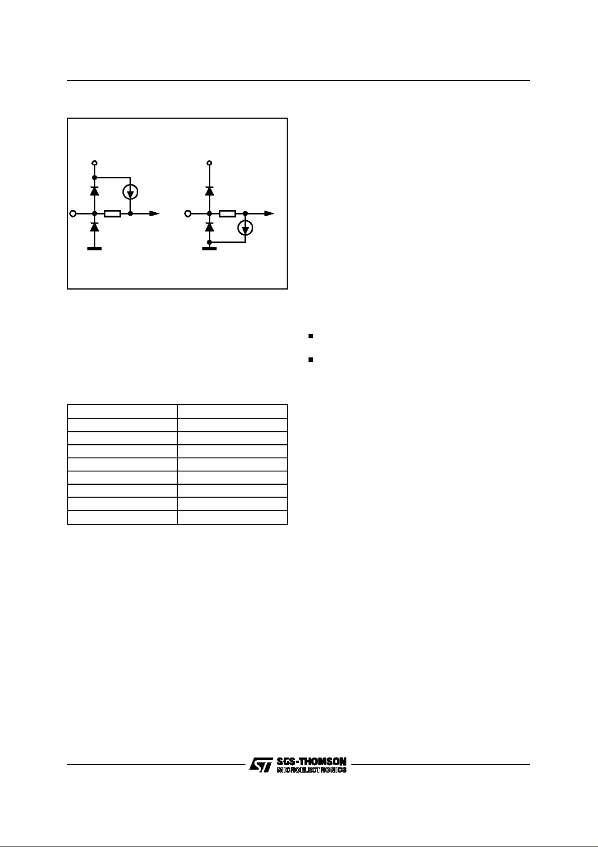
Figure 1-2 depicts the two possible input structures for the logic inputs. If a particular pin is not
360K
14
10K
GAIN1-IN
ERROR
AMP OUTPUT
13
11
36WR28A027A118
CS
100K
GAIN2-IN
DA0Out
10
15
314 31 33
6,7,17,29,39,40
41
GND
POR DLY
CC/2
V
PROG
V
CP2CP1
PUMP
V
D95IN278
Rprogram
0.01µF
1µF
0.068µF
360K
360K
Rs 0.4
OUT
DA2
SENSE OUT
OUT B
12
L6244
VOICE COIL DRIVER
8/31
12V
60-90Hz
Note: If the internal Start-up
Algorithm is not used,
VLOGIC(5V)
connect this pinto SYS_CLK
MONO
GATE
22µF
LOGIC
V
SEQ.
DRV
ANLG
V
PWR
V
ALIGN
F
OUT ENA
38 26
12 39
27 11,42
OUT A
22
10
CTRL
RUN/BRK
V
33
23
43
CTR TAP
SEQ INC
34
1
OUT B
MTR
F
31
OUT C
OT WARM
18
L6238S
36
CONTROLLER
DLY(0)TDLY(1)TDLY(2)
T
16
15
14
SPINDLE MOTOR DRIVER
4.35
346.33
5
CSA
RSENSE
CHRG PUMP 2
10nF
20
8
PWM
TMR
6,7,17,
CHRG PUMP 1
29,39,40
GND
3
BRK
37
GM
44
PWM
CHRG
25 9
SYS CLK
DLY
COMP
SLEW
PUMP 3
10K
4.7µF
220pF
0.1µF
0.068µF
100K
400pF
8.12MHz
L6238S
Figure1-2
V
LOGIC
10µA
330
PULL-UP PULL-DOWN
D95IN279
V
LOGIC
330
10µA
used in an application, it may either be connected
to ground or VLOGICas required, It may also be
simplyleft unconnected.
If no connection is made, the pin is either pulled
high or low by internal constant current generatorsas shownabove.
A listing of the logic and clock inputs is shown in
Table1 with the correspondingdefault state.
Table 1
Pin Function Configuration
Tdly (0,1,2) Pull-Down
Select Pole Pull-Down
PWM/Linear Pull-Down
Output Enable Pull-Down
Run/Brake Pull-Up
Sequence Increment Pull-Down
System Clock Pull-Up
Faling Pull-Up
1.3 Modes ofOperation
Thereare 5 basicmodes of operation.
1) Tristate
When Output Enable is low, the output power
driversare tristated.
2) Start-Up
With Output Enable high, bringing Run/Brake
from a low to a high will energize the motor and
the system will be driven by the Fully-Integrated
StartUpAlgorithm.
A user-defined Start-Up Algorithm, under control
of a MicroProcessor,can also be achieved via the
sequenceincrementinput.
3) Run
Run mode is achieved when the motor speed
(controlled by the external microprocessor)
reaches the nominalspeed.
4) Park
When Run/Brake is brought low, energy to park
the heads may be derivedfrom the rectified Bemf.
The energy recovery time is a function of the
Brake Delay Time Constant. In this state, the quiescent current of the device is minimized (sleep
mode).
5) Brake
After the Energy Recovery Time-Out, the device
is in Brake, with all lower Drivers in full conduction.
There are two mutually exclusive conditions
which may be present during the Tristate Mode
(wake up):
a)the spindleis stopped.
b)the system is still running at a speed that
allows for resynchronization.
In order to minimize the ramp up time, the microcontrollerhas thepossibility to:
check the SPIN SENSE pin, (which toggles at
the Bemf zerocrossing frequency)
enable the power to the motor based on the
previous information.Otherwise the µP may issue a Brake command, followed by the startup procedureafter the motorhas stoppedspinning.
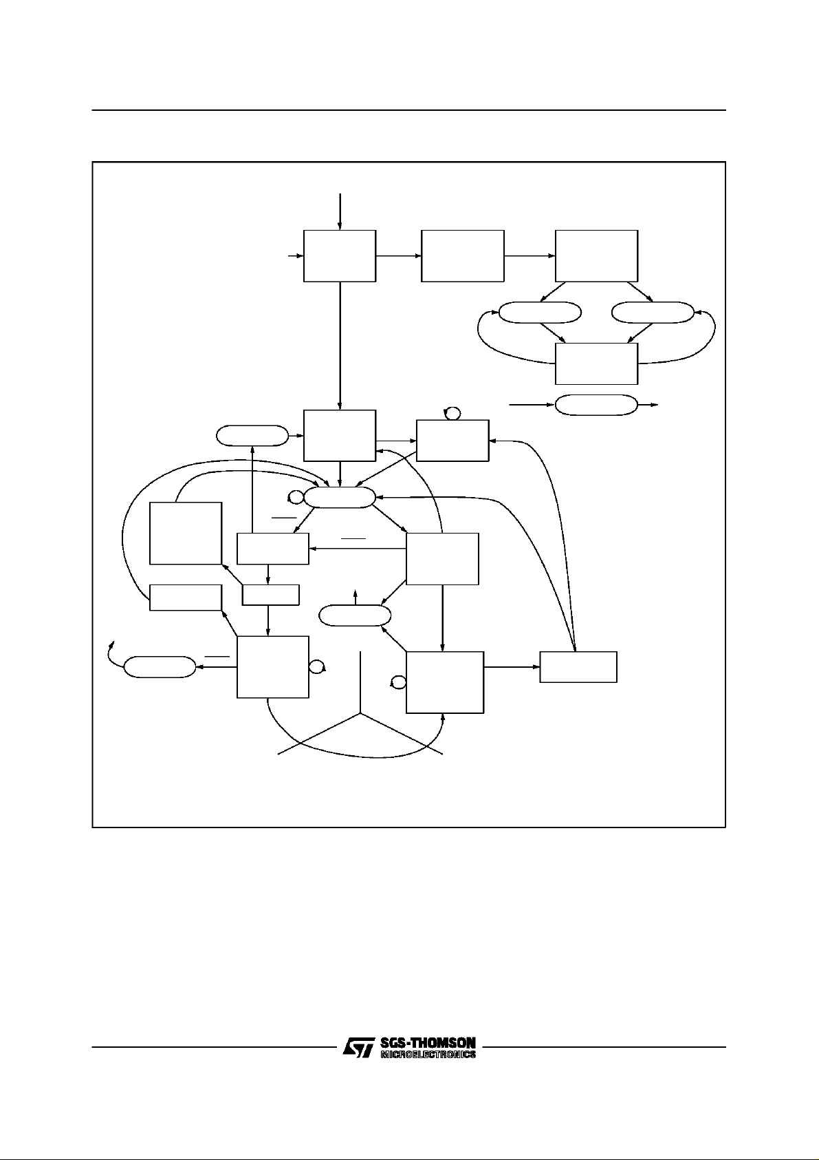
2.0 STATEDIAGRAMS
2.1 StateDiagram
Figure 2-1 is a complete State Diagram of the
controllerdepicting the operationalflow asa function of the control pins and motor status. The flow
can be separatedinto fourdistinct operations.
2.2 Align + Go
Figure 2-2 represent the normal flow that will
achieve a spin-up of the spindle motor using the
internallygenerated start up algorithm.
Upon power up, or from any state with
Run/Brake low the controller first sets the state
machine for State=1with the Outputs Tristated.
The period counter that monitors the time between zero crossing is stopped, analog with the
phase and maskdelay counters.
When Run/Brake is brought high, the motor is in
the firstpart of the align mode at State 2 (Output
A high and Output C low). If Output Enable is
high, thecontrollerfirst checks to determine if the
motor is still spinning for a time of 21Ω (with
Sys_Clk = 10MHz). The drivers are now enabled
and after the align time-out, (64/Falign), the sequencer double increments the outputsto State 4
(Output B high and Output A low). The first part
of this align mode is used to reduce the effectsof
stiction
9/31
L6238S
Figure2-1
RUN/BRK=0
DRIVERS OFF
OUTENA=1
OUTENA=1
DRIVERS OFF
STATE=STATE+1
MIN CLOCK DELAY
LOAD MIN DELAY
LOAD MAX MASK
DELAY COUNT
STATE=STATE+1
MASK COUNT
DRIVERS OFF
MIN CLOCK DELAY
PERIOD STOP
OUTENA=0
SYS_CLK
OUTENA=0
21
2
RUN/BRAKE=0
FROM ANY STATE
STATE=STATE+2
DRIVERS ON
PERIOD STOP
DELAY STOP
MASK STOP
STATE=STATE+2
STATE=STATE+1
LOAD DELAY=MIN
LOAD MASK=MAX
PERIOD COUNT
DELAY COUNT
STATE=STATE+1
MASK COUNT
21
2
SYS_CLK
64/FALIGN
192/FALIGN
POR=0
FROM ANY STATE
(FOR IS GENERATED INTERNALLY
BY MONITORING VLOGIC)
STATE= 1
DRIVERS OFF
MIN CLOCK DELAY
PERIOD STOP
DELAY STOP
MASK STOP
RUN/BRAKE=1
DRIVERS OFF
MIN CLOCK DELAY
LOAD MIN MASK***
PERIOD STOP
DELAY COUNT
STATE=STATE+1
MASK COUNT
OUTENA=1
CHECK FOR ZcBEMF
21
2
SYS_CLK
RUN/BRK=0
DRIVERS OFF
BEMF
SEQLNC=1 &
OUTENA=0
RUN/BRK=X
OUTENA=1
BEMF
RUN
MODE
BEMF
LOAD DELAY=MIN
LOAD MASK=MIN
RESET PERIOD
PERIOD COUNT
DELAY COUNT*
STATE=STATE+1
MASK COUNT
MONO=0**
DRIVERS ON
LOAD DELAY=PERIOD
LOAD MASK=PERIOD
RESET PERIOD
PERIOD COUNT
DELAY COUNT*
STATE=STATE+1
MASK COUNT
INT. START-UP DISABLED
MIN. CLOCK DELAY
LOAD MIN. DELAY
LOAD MIN. MASK***
BEMF
LOAD MIN. DELAY
LOAD MIN. MASK***
DELAY COUNT
STATE=STATE+1
MASK COUNT
BEMF
RUN/BRK=1 &
OUTENA=1
STATE=STATE+1*
MASK COUNT
SEQINC=1
FROM ANY STATE
WITH SEQ_INC=0
OUTENA=1
OUTENA=0
DRIVERS ON
PERIOD COUNT
DELAY COUNT
SEQINC=0 SEQINC=1
BEMF BEMFSEQINC=0 SEQINC=1
LOAD DELAY=PERIOD
LOAD MASK=PERIOD
RESET PERIOD
PERIOD COUNT
DELAY COUNT**
STATE=STATE+1
* VALID IF SEQINC=0, AND DELAY TIMES OUT
** CLOCK DELAY=F(TDLY_[2:0])
WHEN BEMF PERIOD <3.3ms @ 10MHz
(SPEED >12.7Hz FOR 8 POLES)
BEMFOUTENA=1
DRIVERS OFF
MIN CLOCK DELAY
PERIOD STOP
MASK COUNT
RETURN TO
PREVIOUS STATE
(CHANGING SEQINC=1)
ALIGN &
GO MODE
* CLOCK DELAY=F(TDLY [2:0] WHENBEMF PERIOD <3.3ms@ 10MHz (SPEED>12.7Hz FOR 8 POLES)
BEMF: BEMF RISING WITH PNSLOPE=1 OR BEMF FALLING WITH PNSLOPE=0
BEMF1: BEMF RISING WITH PNSLOPE=0 OR BEMF FALLING WITH PNSLOPE=1
**MONO=0 WHEN FREQ(BEMF)=2*FREQ(PHASE)
***MIN MASK=192/SYS_CLK(I.E. WITH SYS_CLK=10MHz,MIN MASK=19.2µs)
BEMF
After the next align time-out 192/Falign), the controller enters the Go mode, were the sequencer
again double increments the output phase upon
detectionof themotor’s Bemf.
The align time-outmay be optimized for the application by changing the Faling reference frequency.
A Watch-Dog Timer protection feature is built into
the control logic to monitor the Falign pin for a
clockingsignal. This circuitry, shown in Figure2-3
will prevent start up the device if the Falign clock
isnot present.
10/31
RESYNCHRONIZATION
MODE
D95IN280
Without this feature, the output would remain in
the first phase under high current conditions, if
the clockwere not present.
If the external sequencer is used to provide start
up, thesystem clock may be tied to the Falign pin
to satisfy the requirements of the Watch-Dog
Timer.
2.3 Resynchronization
If power is momentarily lost, the sequencer can
automatically resynchronize to the monitored

L6238S
Figure2.2
RUN/BRK=0
FROM ANY STATE
Figure2-4
POR=0
FROM ANY STATE
STATE=1
DRIVERS OFF
MIN CLOCK DELAY
PERIOD STOP
DELAY STOP
MASK STOP
RUN/BRAKE=1
DRIVERS OFF
MIN CLOCK DELAY
LOAD MIN DELAY
LOAD MIN MASK
PERIOD STOP
DELAY COUNT
STATE=STATE+1
MASK COUNT
OUTENA=1
CHECK FOR Zc
21
2
SYS_CLK
BEMF: BEMF RISING WITH PNSLOPE=1 OR BEMF FALLING WITH PNSLOPE=0
BEMF: BEMF RISING WITH PNSLOPE=0 OR BEMF FALLING WITH PNSLOPE=1
***MIN MASK=192/SYS_CLK (I.E. WITH SYS_CLK=10MHz, MIN MASK=19.2µs)
DRIVERS ON
PERIOD STOP
DELAY STOP
MASK STOP
64/FALIGN
CHECK FOR Zc
192/FALIGN
STATE=STATE+1
LOAD DELAY=MIN
LOAD MASK=MAX
PERIOD COUNT
DELAY COUNT
STATE=STATE+1
MASK COUNT
BEMF
DRIVERS ON
LOAD DELAY=PERIOD
LOAD MASK=PERIOD
RESET PERIOD
PERIOD COUNT
DELAY COUNT*
STATE=STATE+1
MASK COUNT
BEMF
BEMF
D95IN310
Bemf. This resychronization can either occur
whenever Output Enable or Run/Brake is first
brought low then high.
Referring to figure 2-4, the ”Hold for Resync”
state is brought low. The controller leaves this
state and enters ”Start Resync” when Output En-
able is high.
Figure 2.3: Watch-DogTimer
OVER TEMP SHUTDOWN
S
TO START-UP
Q
LOGIC
Q
S
OUTPUT
ENABLE
RUN/
BRAKE
FALIGN
D95IN311
BEMF
RUN/BRK=0
DRIVERS OFF
BEMF
RUN
MODE
LOAD MIN DELAY
LOAD MIN MASK***
DELAY COUNT
STATE=STATE+1
MASK COUNT
BEMF
CHECK FOR Zc
LOAD DELAY=MIN
LOAD MASK=MIN
PERIOD COUNT
DELAY COUNT*
STATE=STATE+1
MASK COUNT
MONO=0** BEMF
DRIVERS ON
LOAD DELAY=PERIOD
LOAD MASK=PERIOD
RESET PERIOD
PERIOD COUNT
DELAYH COUNT*
STATE=STATE+1
MASK COUNT
RESYNCHRONIZATION MODE
OUTENA=1
BEMF
OUTENA=1
OUTENA=0
BEMF
DRIVERS OFF
MIN CLOCK DELAY
PERIOD STOP
HOLD FOR RESYNC
D95IN312
*CLOCK DELAY=(TDLY [2:0]WHEN BEMF PERIOD <3.3ms @ 10MHz (SPEED>12.7Hz FOR 8 POLES)
BEMF: BEMF RISINGWITH PNSLOPE=1 ORBEMF FALLING WITH PNSLOPE=0
BEMF: BEMF RISINGWITH PNSLOPE=0 ORBEMF FALLING WITH PNSLOPE=1
** MONO=0 WHENFREQ (BEMF)=2*FREQ(PHASE)
*** MIN MASK=192/SYS_CLK(I.E.WITH SYS_CLK=10MHz, MIN MASK=19.2µs)
11/31

L6238S
Figure2-5
SEQINC=0
POR=0
FROM ANY STATE
STATE=1
DRIVERS OFF
MIN CLOCK DELAY
PERIOD STOP
DELAY STOP
MASK STOP
SEQINC=1 &
OUTENA=0
RUN/BRK=X
INT START-UP DISABLED
MIN CLOCK DELAY
LOAD MIN DELAY
LOAD MIN MASK
RUN/BRK=1 &
OUTENA=1
DRIVERS ON
PERIOD COUNT
DELAY COUNT
SEQINC=1
STATE=STATE+1
SEQINC=0
FROM ANY STATE
WITH SEQ_INC=0
MASK COUNT
SEQINC=1
*VALID IF SEQINC=0, ANDDELAY TIMES OUT
**CLOCK DELAY=F(TDLY_[2:0])
WHEN BEMF PERIOD <3.3ms @ 10MHz (SPEED >12.7Hz FOR 8 POLES)
BEMF
LOAD DELAY=PERIOD
LOAD MASK=PERIOD
RESET PERIOD
PERIOD COUNT
DELAY COUNT**
If zero crossings are detected,the sequencer will
automaticallylock on to the properphase.
This resynchronization will take effect with the
motor speed running as low as typically 30% of
it’snominal value.
2.5 ExternalSequencing
Although the user-defined Start-Up Algorithm is
flexible and will consistently spin up a motor with
no external interaction, the possibility exists
where certain applicationsmight require complete
microprocessorcontrol of start-up.
The L6238S offers this capability via the SE-
QUENCE INCREMENT input. Referring to figure
2-5, during initial power-up with Output Enable
low, the controlleris in the ”Hold and Wait for Decision” state. If the SEQUENCE INCREMENT pin
is brought high during this state, the Auto StartUp
Algorithm is disabled and the sequencer can be
controlledexternally.
When Output Enable and Run/Brake are
brought high, the sequencer is incremented on
each positive transition o the SEQUENCER IN-
12/31
MASK COUNT
STATE=STATE+1
BEMF
PREVIOUS STATE
(CHANGING SEQINC=1)
SEQINC=1
RETURN TO
D95IN313
CREMENT pin. During the time that this pin is
high, all Bemf information is masked out. Whenit
is low, the Bemf informationcan be detected normally after the internal mask time. The minimum
mask time is 192/Sys_Clk (i.e. with Sys_Clk =
10MHz, min. mask = 19.2µs) Therefore to insure
that the sequencer is under complete control of
the state machine, the time that the SEQUENCE
INCREMENT pin is held lowshould be much less
then the min. mask time,but greater then1µs.
When the motor has reached a predetermined
speed, the SEQUENCE INCREMENT pin can be
left low and the L6238S Motor Control logic will
take over and automatically spin up the motor to
the desiredspeed
.
3.0 START-UPALGORITHMS
3.1 Spin-UpOperation
The spin operationcan be separatedinto 3 parts:
1) Open Loop Start-Up - The object is to create
motion in the desired direction so that the Bemf
voltages at the3 motor terminals can providereliable information enabling a transition to closed
loop operation.

Figure3-1: Align+Go
L6238S
RUN/BRAKE
SEQUENCER
A
OUT
10V
1
B
OUT
10V
2
C
OUT
10V
3
ALIGNMENT GO
*0.711s *2.133s
STATE 2
A=HIGH
B=FLOAT
C=LOW
DOUBLE INCREMENTS
STATE 4
A=LOW
B=HIGH
C=FLOAT
STATE 6
A=FLOAT
B=LOW
C=HIGH
2) Closed Loop Start-Up - The Bemf voltage
zerocrossings provide timing information so that
the motor can be accelerated to steady state
speed.
3) Steady-State Operation - The Bemf voltage
zero-crossings provide timing information for precisionspeed control.
The L6238S contains features that offer flexible
control over the start-upprocedure. Either the onboard Auto-StartAlgorithm can be used to control
the start-up sequence or more sophisticated extenal start-up algorithms can be developedusing
the Serial Port and key control/sense functions
broughtout to pins.
3.2 Auto-Start Algorithm
When initially powered up, the controller defaults
to the internal AutoStart Mode. When Run/Brake
is low, the L6238S is in brake mode, and the
Auto-Start Algorithm is reset. In the brake mode,
all of the lower DMOS drivers are ON,and the up-
500ms/DIV* FALIGN=90Hz
D95IN314
per drivers are OFF.
The Auto-Start Algorithm is based on an Align &
Go approachand can be visualized by referringto
Figure 3-1. Shown are the Run/Brake controlsignals, sequencer function, and the three output
voltage waveforms.
Referring to figure 3-1, the following is the sequence of events duringAuto-Start:
With Output Enable =1,Run/Brake =0
- State Machine is set to State 1 with the drivers
Trisatted.
AlignmentPhase (1)
Run/Brake =1
- Output Stageis sequencedto State 2 and the
drivers energized with OUTPUT A high and
OUTPUT C low for 64/Falignseconds.
AlignmentPhase (2)
- Output Stage is double sequenced to State 4
with OUTPUT B high and OUTPUT A lowfor
13/31

L6238S
192/Falign seconds.
- During the alignment phase, the SEQ INCRE-
MENT signalis ignored.
Go Phase
- The internal sequencer double increments the
output stage to State 6, whichshould produce
torque in the desireddirection.
- with SEQ INCREMENT held low, the se-
quencer is now controlled by the Bemf zero
crossings, and the motor should ramp up to
speed.
3.3 ExternallyControlled Start-Up Algorithms
Enhanced Start-Up Algorithms can be achieved
by using a µProcessor to interact with the
L6238S.’ The L6238S has the ability to transition
to Closed Loop Start-Up at very low speeds, reducing the uProcessor task to monitoring status
rather than real time interaction.Thus, it is a perfectapplication for an existing µProcessor.
The following control and status signals allow for
very flexiblealgorithm development:
SEQ_INCR A low tohigh transitionat thisinput
isused to increment the state of thepower output stage. It is useful during start-up, because
the µProcessor can cycle to anydesired state,
or cycle through the states at any desiredrate.
When held high, it inhibits the BEMF zero
crossings from incrementing the internal sequencer.
SPIN SENSE This output is low until the first
detected Bemf zero crossing occurs. It then
toggles at each successivezero crossing.This
signal serves as a motion detector and gives
useful timing information as well as the slope
of the Bemf.
3.4 Start UpApproaches
Align & Go Approach The Align & Go approach
provides a very time efficient algorithm by energizing the coils to align the rotor and stator to a
known phase. This approach can be achievedvia
the sequencingSEQINCR. SPIN SENSE can be
monitored to assure that motion occurred. Once
ample time is given for alignment to occur, SEQ
INCR can be double incremented, and the SPIN
SENSE pincan be monitored todetect motion.
When SEQ INCR is pulled low, control is transferred to the internal sequencer, and the L6238S
finishes the spinup operation. If no motion is detected, SEQINCR can be incrementedto a different phase and the process can be repeated.The
alignment phase may cause backward rotation,
which on the average will be greater than the
StepperMotor approach.
The Auto-Start algorithm described earlier is an
Align & Go approach. The main advantages of
the integratedAuto-Start are that the µP is not involved real-time, and there are a minimum of interface pins required to the spindle control system.
Stepper Motor Approach This approach minimizes backward rotation by sequencing SEQ
INCR at an initial rate that the rotor can follow.
Thus, it is driven in a similar fashion to a stepper
motor. The rate is continually increased until the
Bemf voltage is large enough to reliably use the
zero-crossings for commutation timing. SEQ
INCR is held low, causing control to be passed to
the L6238S’sinternal sequencer as in the Align &
Go approach.
The Stepper Motor approach takes longer than
the Align & Go approach because the initial commutation frequency and subsequent ramp rate
must be low enough so that the motor can follow
without slipping. This implies that to have a reliable algorithm, the initial frequency and ramp rate
must be chosen for the worst case motor under
worst case conditions.
4.0 MOTORDRIVER
4.1 Output Stage
The output stage forms a 3-Phasefullwave bridge
consisting of six Power DMOS FET High output
currents are allowed for bbrief periods. High output currents are allowed for brief periods. Output
Power exceeding the stand-alone power dissipation capabilities of the L6238S can be increased
with the addition of an external P-FET or by the
use of Pulse-Width-Modulation.
Table 4-1 is a reference diagram that liststhe parameters associated with 8-pole motors operating
at 3600 and 5400 RPM.
Figure 4-1 represents the waveforms associated
with the output stage. The upper portion of figure
4-1 shows the flow of current in the motor windings for each of the 24 phase increments. A rotational degree index is shown as a referencealong
with a base line to indicate the occurrence of a
zero crosing. The outputwaveforms are a digitally
reproduced voltage signals as measured on samples.The feedback Input is multiplexed between
the internal Bemf Zero Crossing Detector and an
externallyprovided sync pulse (EXTINDEX)
Shown in figure 10 is the classical state diagram
for a phase detector along with waveform examples.
A typical sequence starts when the outputs
switch states. Referring to figure 4-1, during
phase 1, output A goes high, while outputBis low.
During this phase, output C is floating, and the
Bemf is monitored. The outputs remain in this
state for 60 electrical degrees as indicated by the
first set of dashed lines. After this period the out-
14/31

Table 4-1
L6238S
Rotational Speed 3600rpm 5400rpm
Rotational Frequency 60Hz 90Hz
Rotational Period 16.667ms 11.111ms
Electrical Period 4.167ms 2.778ms
Phase Period 694.5µs 463.0
Figure4-1: Waveforms
15/31

L6238S
put switched to phase 2 with output A high and C
lowwith the Bemfamplifier monitoring outputB.
In order to prevent commutation currentnoise being detectedm as a false zero crossing, a masking circuit automatically blanks out all incoming
signals as soon as a zero crossing is detected.
When the next commutation occurs an internal
counter starts counting down to set the time that
the maskingpulse remains.
The counter is initially loaded with a number that
isequal to time thatis always25% of the previous
phase period or 15 electrical degrees. The timeout of the masking pulse shown for reference at
the bottom of figure 4-1. Thus the actual masking
period is the total of the time from the detected
zero crossing to the phase commutation, plus
25% of the previous period. The mask pulse operation is further discussed in section 4.6, Slew
RateControl and PWM operation.
Afterthe maskingperiod, the Bemfvoltage at output B is monitored for a zero crossing. Upon detection of the crossing, the output is commutated
after the selected phase delay insuring maximum
Figure4-2
torque. The spin sense waveform atthe bottom of
the figure indicates that this output signal toggles
with each zero crossing.
4.2 Brake Delay
When Run/Brake is brought low, a brake is initiated. Referring to figure 4-2, SW1 is opened and
the brake delay capacitor, C
discharge towardsgroun via R
, is allowed to
brake
.
brake
At the same time, switches SW2 through SW7
bring the gates of the output FETs to groundhalting conduction,causing the motor to coast. While
the motor is coasting, the Bemf is used to park
the heads. When Cbrake reaches a voltage that
is below the turn ON threshold of Q1, Switches
SW8, 9, and 10 bring the gates of the lower drivers to V
potential. This enables the lower
brake
FETs causing abraking action.
The analog and logic suppliesare not monitored
in the L6238S, since the L6244 alreadymonitors
this voltage and initiates a Park function when
either supply dropsto a predeterminatedlevel.
16/31

Figure4-3
L6238S
4.3 Charge Pump
The charge pump circuitry is used as a means of
doubling the analog supply voltage in order to allow the upper N-channel DMOS transistors to be
driven like P-channel devices. The energy stored
in the reservoircapacitor is also used to drive the
lower driversin a brakemode if the analog supply
is lost. Figure 4-3 is a simplifiedschematiocof the
chargepump circuitry.
Figure4-4
SW2
UPPER A
VCTRL
+
A2
-
LOWER A
A3
SW3
1
0
I2
Islew
X4
VANALOG
A capacitor, C
, is used to retrieve energy
pump
from the analog supply and then ”pumps” it into
the storage capacitor,C
resvr
.
An internal300KHz oscillatorfirst turns ON Q2 to
quickly charge C
to approximately the rail
pump
voltage. The oscillator then turns ON Q1 while
turning OFF Q2. Since the bottom plate of C
is now effectivelyat therailvoltage via D2.
A zener-referencedseries-pass regulatorsupplies
OUTPUT
BC
L1 L2
L3
OUTA
RSENSE
CSA
R
S
V
PUMP
1
0
VPOWER
Q1
Cfet
I1
Islew
Q2
Cfet
pump
,
Q3 Q4
REFERENCE CURRENT
Q5
PWM SLEW/RC
R
SLW
3.1VSLEW RATE
D95IN315
17/31

L6238S
a voltage,V
, duringbrakemode.
brake
The maximum capacitance specified for the Storage Capacitor is 4.7µF.For applications requiring
a larger value, an external diode should be connected between Vanalog and the Storage Capacitor to prevent excessive inrush current from
damaging the charge pump circuitry. A small
value resistor (i.e. 50W) may instead be inserted
in series with the StorageCapacitorto limit the inrushcurrent.
4.4 Linear Motor CurrentControl
The output current is controlled in alinear fashion
via a transconductanceloop. Referring to Figure
4-4 the sourcing FET of one phase is forced into
full conduction by connecting the gate to V
pump
while the sinking transistor of an appropriate
phase operates as a transconductance element.
To understand the current control loop, it will be
assumed that Q2in figure 4-4 is enabled via SW3
by the sequencer. Duringa run condition, the currentin Q2 ismonitored by a resistorR
to the R
sense
input.
The resulting voltage that appears across R
connected
s
s
amplified by a factor of four by A3 and is sent to
A2where it is compared to the CurrentCommand
Signal. A2 provides sufficientdrive to Q2 in order
to maintain the motor speed at the proper levelas
commandedby the Speed Controller.
The pole/zero locations are adjusted such that a
few dB of gain (typ. 20dB) remains in the transconductanceloop at frequencieshigher than the
zero.
The inductive characteristic of the load provides
the pole necessary for loop stability. Thus the
loop bandwidth is actually limited by the motor itself.
Figure 4-5 shows the completetransconductance
loop including compensation, plus the response.
The Bode plot depicts the normal way to achieve
stability in the loop. The pole andzero are used to
set a gain of 20dB at a higher frequency and the
pole of the motor cuts the gain to achieve stability.
Loop instability maybe causedby two factors:
,
1)The motorpole is tooclose to thezero. Referring to figure 4.6, the zero is not able to decrementthe shiftof phase, and when the effect
of the pole is present, the phase shift may
reach 180° and the loop will oscillate. To rectify this situation, the pole/zero must be
shifted at lower frequencies by increasing the
is
compensationcapacitor.
Figure 4-6
4.5 TransconductanceLoop Stability
The RC network connected to the Compensation
pin provides for a single pole/zero compensation
scheme. The pole/zero compensation scheme.
Figure4-5
Figure 4-7
18/31

L6238S
Figure4-8
2)The motor capacitance, CM, itself can interfere with the loop, creating double poles. If
the gain at higher frequencies is sufficiently
high, the double pole slope of 40dB/decade
can cause the phase shift to reach 180°,
re sulting in oscillation.
Figure 4-8 is a Bode plot showing how to correct
this situation.The bold line indicates the response
with relatively high gain at the higher frequencies.
Byleaving the pole unchangedand increasingthe
zero, the response indicated by the dashed lines
canbe achieved.
4.6 SlewRate Control
A 3-phase motor appears as an inductive load to
the power supply. The power supply sees a dis-
turbance when one motor phase turns OFF and
another turns ON because the FET turn-OFFtime
is much shorter than the L/R rise time. Abrupt
FET turn-OFF without a proper snubbing circuit
can even cause current recirculationback intothe
supply.
However, the need for a snubber circuit can be
eliminated by controlling the turn-OFF time of the
FETs.
The rate at which the upper and lower driversturn
OFF is programmable via an external resistor,
connected to the SLEW RATE pin. This re-
S
slew
sistor defines an internal current source that is
utilized to limit the voltage slewrate at theoutputs
during transition, thus minimizing the load change
that the powersupply sees.
To insure proper operation the range of resistor
values indicated should not be exceeded and in
some applications values near the end points
should be avoidedas discussed below.
Low Values of Rslew - If a relativelylow valueof
Rslew is selected, the resultant fast slew rate will
result in increased commutation cross-over current, higher EMI, and large amount of commutation current.
This last case can cause voltage spikes at the
output that can go as much as lV below ground
level. This situation must be avoided in this integrated circuit (as in most) since it causes unpredictable operation.
High Values of Rslew - Higher values of Rslew
result of course in slow slew rates at the outputs
which is, under most conditions, the desired case
since the problemsassociated with fast rates are
reduced. The additional advantage is lower
acoustical noise.
Problems can occur though if the slew rate for a
Figure4-9: Effect of Slow Slew Rate.
19/31

L6238S
Figure4-10: ExternalP-Fet.
given application is too slow. Figure 4-9 is an oscillographtaken on a device thathad a fairlylarge
value for Rslew and failed to spin up and phase
lock a motor.
The problem manifests itself as the motor begins
to spin up.At lowerRPMs, the Bemf of the motor
is relatively small resulting in higher amounts of
commutation current. In figure 4-9, the upper
waveform is the voltage appearing at OUTPUT
relative to the CENTER TAP input. The lower
waveform is the actual output of the Bemf amplifier availableon specialengineering prototypes.
The oscillograph was taken just as the problem
occured. The period between zero crossings was
~800µsresulting in a masktime period of 200µs.
As can be seen, the excessively long slew rate
actually exceeded the mask period and was detected as a zerocrossing.
This resulted in improper sequencing of the outputsrelative to the proper phases and caused the
motor to spindown.
4.7 Ext PFETDriver
The power handling capabilities of the 3 phase
output stage can be extended with the addition of
a single P-ChannelFET.
Figure 4-10 shows the Ext FET connection and
demonstrates how the L6238S automatically
senses the FETs presence. When the voltage at
the Gate Drive pin is ≥ 0.7V, the output of comparator A3 goes high, removing the variable drive
A1 from the internal FETs and connects them instead to Vanalogvia thecommutation switches to
facilitate full conduction.
The upper FETs drive paths are not shown for
clarity. A3 also closes SW2 allowing A1 to linearly
drive the external P-Channel FET Q1 via inverter
A2.
4.8 Bemf Ampolifier
Since no Hall Effect Sensors are required, the
commutation informationis derived from the Bemf
voltage zero-crossingsof the undriven phase with
respect to the center tap. The Bemf comparator
and associatedsignal levels are depicted in figure
4-11. For reliable operation, the Bemf signal amplitude should be a minimum of ± 60 mV to be
properly detected. In order to provide for noise
immunity, internal hysteresis is incorporated in
the detectioncircuitry to prevent false zero crossing detection.
For laboratory evaluation purposes, a simple re-
20/31

Figure 4-11:Bemf Amplifier.
Vo
BEMF
-35 -25 0 25 35
SLOPE=0 SLOPE=1
Vi
D95IN316
L6238S
BEMF(mV)
sistive network as shown in figure 4.12 can be
usedto emulatethe Bemf ofthe motor.
The actual Bemf zero-crossingis 30 electrical degrees (50% of a commutation interval) away from
the optimal switch point. A digital counter circuit
measures 50% of the previous interval to determine the next interval’s commutation delay from
the zero crossing. During the low RPM stages of
start up the long commutation intervals may
cause the counter to overflow, in whichcase 50%
of the max count will be less than 50% of the
ideal commutation interval. Therefore, the torque
Figure4-12: Bemf Emulator
will not be optimal until the desired commutation
interval is less than the dynamic range of the
counter.
4.9 Center TapProtection
Spindle Motors with a high number of windings
exhibit a transformer coupling effect that in some
cases can cause relatively high currents to flow
through the centertap input.
Current flowing out of the center tap pin as high
as 25mA has been observed with certain motors.
Figure 4-13
TO CENTER
R1 1K
TAP INPUT
D95IN317
DS1
21/31

L6238S
The high current flows from the grounded substrate of the integrated circuit (p-type material),
throughone ormoreepitaxialpockets(n-type material)and outthecenterpar pin.
This current can cause adverse operation of the
controllet due to substrate injection and might
possibility damage the internal metalization runs.
The normal current for this input is in the 200µA
range.
Referring to figure 4-13, a simple protection
scheme consisting of a 1K resistor and a low current Schottky diode should be added if the application causes excessive current (i.e. >1mA) to
flow throughthe center tap pin.
5.0 PWM MOTOR CURRENTCONTROL
A unique feature of the L6238S in the optional
Pulse Width Modulation (PWM) control of motor
current.
Using Variable-frequency, Constant-OFF time
Current-Mode control, the L6238S can drive
higher power motorswithout the need forexternal
drivers, while minimizing internal power dissipation.
Additional benefits include reduced power supply
consumption(up to 50% savings)and lowerwattage requirementsfor the current sensingresistor.
Constant-OFF time Current-Mode control, operates on the principle of monitoring the motor current and comparison it to a reference or control
level.
When the motorcurrent reachesthis commanded
level, the output drivers turn OFF and remain
OFFfor a Constant-OFFtime. After this OFF time
the drivers turn backONto repeatthe cycle.
Figure 5.1 is a block diagram of the PWM control
circuitry. When using PWM as opposed to linear
control, two changes are made to the control
loop:
1.The slew rate control is disabled,allowing the
outputs to slew at a minimum rate of 10V/µs.
This is accomplished by closing SW3 and
SW5.
2.The OTA amplifier is taken out of the control
loop via SW6. The lower drivers are now
driven into hard conductionby tying the gates
to the analog supply during the On time of the
PWM cycle.
The current in the motor windingsis monitoredvia
the voltage dropped in the sensing resistor,
.
R
sense
This voltage is multiplied by a factor of 4 in the
Current Sense Amplifier (CSA) and sent to negative input of the PWMComparator (A2).
The control voltage,V
, isapplied to the posi-
control
tive input of A2. When the output of the CSA
reaches a level that is equal to the commanded
level, the output of A2 switches low, toggling the
latch comprised of N1 and N2. This causes the
upper drivers to turn off andopens SW1. Q3 turns
OFF allowing the Constant-OFF time capacitors,
Figure5-1
PWM/SLEW
COFFRSLEW
VANALOG
SLEW RATE
REFERENCE
CURRENT
Q3
1.2V
3.1V
PWM/LIN
CONTROL
SW1
+
A1
-
UPPER A
LOWER A
N1
N2
N3Q1 Q2
SW3
SW5
A3
SW2
SW4
A2
VPOWER
V
PUMP
1
0
I1
Islew
1
0
Islew
+
-
CSA
Cfet
I2
V
ANALOG
SW6
FROM TRANS. LOOP
X4
1
0
Q4
Cfet
Q5
D95IN318
OUTPUT
BC
L1 L2
L3
OUTA
RSENSE
VCTRL
CSA
R
SLW
22/31

C
to discharge to dischargtethrough R
off
slew
, initiating the Constant-OFF time-out. When the voltage on C
reaches 1.2V,comparator A1switches
off
state toggling the latch in the opposite state, turning the upper driver back ON. SW1 also closed
quicklycharging up C
for the nextcycle.
off
5.1 PWM DesignConsiderations
In order to select the parameters associated with
PWM operation, the following factors must be
takeninto consideration:
1. PWM SwitchingFrequency
2.Duty Cycle
3. Motor Currents
4. Minimum ON Time
5.Noise Blanking
6. Bemf Masking/Sampling
5.1.1. PWM Switching Frequency
The PWM switching frequency F
pwm
is found
from:
F
pwm
1
=
+ T
T
on
off
(5.1.1)
where:
= The time requiredfor the motor current
T
on
to reach the commandedlevel.
T
= The programmedOFF time.
off
The two main considerations for this parameter
are the minimum and maximum switching frequency.
The maximum switching frequency occurs during
the Start-upand should be keptbelow 50KHzdue
tointentional bandwidth limitations and output
switching losses.
5.1.2 Duty Cycle
Besides reducing the power dissipation of the
controller output stage, running in PWM offers 2
additional”free” benefits:
A. ReducedPowe SupplyCurrent at StartUp
B. Lower PowerRating for the Motor Current
SenseResistor.
Figure 5-2 is the current path during the ON time
of a phase period. The current from the supply
passes through the upper sourcing DMOS, Q3
transistor through the two driven winding, the
lower DMOS, Q2 and finally through the current
sensing resistor R
. Since both Q3 and Q4 are
sns
ON, while Q3 is turnedOFF. The voltage, causing
the current to continue to flow through Q2, and
Q4.
If the duty cycle is nearor at 50%, then for 1/2 the
PWM cycle, no current is flowing from the power
supply or the sense resistor while current is still
flowing in the motor. This lowers the requirement
L6238S
Figure 5-2
V
POWER
Q1
Q2
D1
L1 L2
OUTPUTA OUTPUTB
D2
R
R
SNS
D3
D4
SENSE
D95IN319
Figure 5-3
V
POWER
Q1
Q2
D1
L1 L2
OUTPUTA OUTPUTB
D2
R
R
SNS
D3
D4
SENSE
D95IN320
for both the Power Supply and the Power Rating
for the sensing resistor.
5.1.3 Motor Currents
Note: It is not theobjective of thissection to describe the principles
of brushless DCmotor, but to provide sufficient information about the
parameters associated with PWMoperation in order to optimizean
application.
A simplified modelof a motor is shown in figure 5-
4. For this discussion, lower order effects due to
mutual inductance between windings, resistance
due to losses in the magnetic circuit, etc. are not
shown.
The motor at stall is equalto a resistance, Rmtr,
in serieswith aninductance, Lmtr. When the mo-
tor is rotating, there is an induced emf that appears across the armaure terminals and is shown
in figure 5-4 as an internally generated voltage
Ibemf), Eg.
Q3
Q4
Q3
Q4
23/31

L6238S
Figure5-4
Lmtr
Rmtr
+
Eg
-
D95IN321
Therelation between thesevariablesis given by:
V = L
mtr
dt
R
mtrimtr
+ E
g
(5.1.2)
di
mtr
where:
V = AppliedVoltage
i
= Motor Current
mtr
= Total inductance of the motor
L
mtr
windings
= Resistancein serieswith the motor
R
mtr
E
= The internally generated voltage of
g
the motor, proportional to the motor
velocity
Since:
E
=KEω (5.1.3)
g
The above equations can be combined to form
the basicelectrical equation fora motor:
di
mtr
dt
mtr
R
mtrimtr
+ KEω (5.1.4)
V = L
Figure 5.5 is a simplified electrical equivalent of
the output stage of the L6238S along with the
model of the motor during the time that the OutputDrives areconducting.
Figure5-5
UPPER
Rdson
Lmtr
The additionalresistance associated with the output stage and sensing resistor are also in series
with the motor. If we let R
equal the total series
s
resistence:
R
= 2*R
s
dsON+Rmtr+Rsense
(5.1.5)
then (5.1.4) becomes:
di
mtr
dt
mtr
Rsi
mtr
+ E
g
(5.1.6)
V = L
Figure 5-6
Lmtr
Rmtr
-
KEW
+
LOWER
Rdson
D95IN323
LOWER
Rdson
Figure 5-6 is an equivalent circuit of the output
stage during the Constant-OFFperiod. During the
OFF time the lower driver for the particular phase
beign drivenremains ON.
The internally generated voltage forces the path
of current though the motor, its series resistance,
the RdsONof the LowerDriver and finallythrough
the oppositelowerdriver.
PWM Example (Referto Figure5-7)
The following is an example on how to select the
timing parameters.
Given:
DCStartCurrent = 1.25A
RippleCurrent = 100mA
Duty Cycle = 50%
24/31
D95IN322
KEW
Rmtr
+
LOWER
Rdson
Rsense
Motor Interface(L) = 880µH
TotalSeries Resistance(R
) = 4.8Ω
s
If the worst case start current is 1.25A and the
duty cycle is 50%, then the Peak Current, It will
be:
= 1.25+
i
t
0.1
2
it=1.30A

L6238S
TheValley current, Ibwill thereforebe:
i
= 1.30 - 0.1A
b
i
= 1.20A
b
During the Align and Go Phase (where the power
dissipation requirements are highest, Eg is zero.
The initial time required to reachthe Peak current
is:
± L
=
t
init
ln
1 ±
R
I,R
V
(5.1.7)
Substitutingvalues:
=
t
init
t
=134.6µs
init
± 880e
4.8
± 6
1.3 ⋅ 4.8
±
ln
1
12
The ON timecan be calculated from:
L
t
=
on
ln
R
s
V
± i
b
R
s
V
± i
t
R
s
(5.1.8)
Substitutingvalues:
± 1.2
± 1.3
t
on
880E ± 6
=
4.8
12
4.8
ln
12
4.8
the voltage drop remains constant across the
windings.
The time required for the inductor currentto reach
the valleycurrent is given by:
I
ln
t
I
b
(5.1.9)
L
=
t
off
R
Substitutingvalues:
±6
880e
=
t
off
4.8
t
= 14.67µs
off
Note: thatthe parameters forthis examplewere selected to arrive at
a 50%duty cycle. This will notalways be thecase due to factors such
as fixed motorparameters, etc.
1.3
ln
1.2
The Constant Off timer period can be determined
from:
V
= R
t
off
slew
⋅ C
off
⋅ ln
V
chrg
trip
(5.1.10)
Where:
= Constant-OFFTime
T
off
= Slew Rate Resistor
R
slew
C
= Off Time Capacitor
off
V
= Initial Capacitor ChargeVoltage
chrg
= Capacitor Lower Trip Threshold
V
trip
Substitutingnominal valuesgiven:
t
=14.67µs
on
Figure5-7
D95IN324
It=1.3A
Ib=1.2A
Iavg=1.25A
Iout A
200mA
4
20µs/DIV
During the OFFtime, the motor currentcontinues
to flow through the DMOS transistorsand threfore
=0.75 ⋅R
T
off
Solving for C
T
=
0.75R
off
C
off
off
slew
slew
⋅ C
off
In the example, to set the OFF timer for a 50%
duty cycle:
Given:
T
= 14.67µs
off
= 100KΩ (typicalValue)
R
slew
C
off
C
off
14.67e
=
≈ 146pF
100e
±6
3
5.1.4 Minimum ONTime
The bandwidth of the PWMloop was optimizedto
reject unwanted switching noise while providing
25/31

L6238S
sufficient response, commensurate with the
switching speed of the output drivers. At higher
frequencies the switching losses inherent in the
drivers start to negativeany of the power dissipationsavingsgained with PWMoperation.
The current sense amplifier has a minimum slew
rate of 0.31V/µs. With a worst case Motor peak
start-up current of 2.5A and Sense Resistor of
0.33, the resultant R
voltage would be equal
sense
to 825mV. With a minimum gain of 3.8V/V, the
CSA output voltage would have to slew to 3.14V.
Therefore it wouldrequire approximately10µs for
the output voltage to reach the required commanded level.
If an ON time were selected that was less than
this time, the motor current would overshoot the
desired level resulting in incorrect current control
possibly exceeding the output capabilities of the
drivers.
5.1.5 Noise Blanking
Referring to Figure 5-8, when operating with
lower levels of current (i.e. < 700mA, with Rsense
= 0.33Ω), the possibility exiss where the noise
due to output Turn-ON can exceed the Commanded Current Level causing prematire TurnOFF.
In order to provide noise immunity from this
switching noise, a blanking circuit automatically
rejects any signal appearing at the output of the
CSA fora 3µs period.
Figure 5-9 is an additional block diagram of the
PWM controlloop includingthe noise blanking circuit. The output of A3 goes high when ever the
voltage at theCSA input is more positive then the
Control Voltage.
This is the case when either the motor current or
the turn-ON transient has reached the commanded level. The output of A3 is gates by N11.
In order to providea blankingperiod, Q1 is turned
Figure 5-8
D95IN325
3µs BLANKING PULSE
COMMANDED
CURRENT LEVEL
Vrsense
1
10µs/DIV
Figure5-9
CLK_BEMF
2.4V
SW1
N12
N1
C1
8pF
5µA
N2
Q1
I1
N3
N4
PWM/LIN
DELAY
TO OUPUT
DRIVERS
N5
N6
N7
N8
I2
20µA
RUN/BRAKE
Q2
N12
N9
N10
N11
+
A2
- 1.2V
A3
+
-
Q3
X4
D95IN326
PWM_SLEW
R1
CSA INPUT
VCONTROL
PWM COMP
PWM TIMER
C4
C3
26/31

L6238S
ONduring the Constant-OFFtime, chargingC1 to
the internal rail. At the end of the OFFtime, Q1 is
turned OFF allowing current source I1 to discharge the capacitor towards ground. While the
voltage on C1 is above the low input threshold of
N1, the output of N1 is low, preventing any
change of state at the output of N11 due toa high
A3output. Whenthe capacitor reachesthe lowinput threshold of N1, N1 chnges state allowing A3
to controlthe stateof N11.
5.1.6 Masking/Bemf Sampling inPWM
The method of sampling the floatingphase for the
bemf zero crossing defers between Linear and
PWMoperation. In Linear Mode, the bemf is sampled continuously after the mask time-out, until
the zero crossing is detected. Then the mask is
enabled for a time based on the commutation
phase delayplus theadditional timebased on the
previousperiod as explained earlier.
With PWM operation however, the switching
noise at turn ON (after the Constant-OFF time)
can be significant, especially at low RPMs where
the bemf is the lowest. In order to provide the
greatest noise immunity in PWM, the floating
phase is monitored only at the point where the
output isabout to be turnedOFF.
In operation, when the motor current reaches the
commandedlevel, the floatingphase is first monitored to determine if the bemf has crossed the
zero. The output is then turned OFF for the Constant-OFFtime out.
As the motor current increases through, the increasing bemf causes the motor current to naturally decrease. Eventually a point is reached
where the PWM is running at 100% duty cycle
and the motor current cannot reach the commanded level. At this time the bemf is no longer
smpled, preventing further commutation of the
output.
The PWM Limit Timer is used to set up a maximum ON time. When this limit is exceeded the
method of sensing the bemf is essentially the
same as in the case ofoperatingin linearmode.
Figure 5-10 is an oscillographof the controlleroperating in PWM mode. The top trace is A
out
. The
2nd trace is the voltage seen at the PWM/SLEW
pin indicating the exponential discharging of the
timing capacitor during the OFF time. Trace 3 is
the voltageappearing on the PWM Timercapacitor, while trace 4 is the motor current.
Referring again to Figure 5-9, and 5-10 transistor
Q2 is turned ON at the beginningof the OFF time,
discharging the external capacitor C4 to near
ground level. At the end of the OFF-Time, Q2 is
turned off and C4 starts charging linearly via I2.
C4 is again discharged at the beginning of the
OFF time and the cycle repeats. As long as C4
does not reach the threshold of A1 (typically
3.5V), the bemf is only sampled just before turnoff of the output. As the motor isstartingup in figure 5-10, the duty cycle is roughly 50%. The
PWM limit timer is reset to ground by the start of
the OFFtimer before reaching the 3.5V threshold.
In figure 5-11, as the motor spins up, the on time
of the output increases and the PWM limit timer
reaches the 3.5V. Eventually the duty cycle
reaches 100% and the sampling of the bemf is
essentiallythe sameas in the linear mode.
The selectionof componentsfor the PWM timer is
not critical. Since the objective is to sample the
bemf only at turn OFF to maximize the signal to
noise ratio, the PWM timer slope canbe set up to
convert to thefull bemfsampling aftera few revolutions of the motor when the bemf has reached
an appropriatevoltage output.
Figure5-10
1
PWM/Slew
2
PWM Limit
Timer
3
4
500mV
Iout A
Aout
10v
2V
1A
Fpwm=50KHz
Coff=120pF
Ctmr=220pF
20µs/DIV
D95IN327
Figure 5-11
10V
1
PWM/Slew
2
PWM Limit
Timer
500mV
3
Iout A
4
Aout
2V
1A
D95IN328
Fpwm=12KHz
Coff=120pF
Ctmr=220pF
50µs/DIV
27/31

L6238S
PLCC44PACKAGE MECHANICAL DATA
DIM.
MIN. TYP. MAX. MIN. TYP. MAX.
A 17.4 17.65 0.685 0.695
B 16.51 16.65 0.650 0.656
C 3.65 3.7 0.144 0.146
D 4.2 4.57 0.165 0.180
d1 2.59 2.74 0.102 0.108
d2 0.68 0.027
E 14.99 16 0.590 0.630
e 1.27 0.050
e3 12.7 0.500
F 0.46 0.018
F1 0.71 0.028
G 0.101 0.004
M 1.16 0.046
M1 1.14 0.045
mm inch
28/31

PQFP44PACKAGE MECHANICAL DATA
L6238S
DIM.
mm inch
MIN. TYP. MAX. MIN. TYP. MAX.
A 3.40 0.134
A1 0.25 0.010
A2 2.55 2.80 3.05 0.100 0.110 0.120
B 0.35 0.50 0.0138 0.0197
C 0.13 0.23 0.005 0.009
D 16.95 17.20 17.45 0.667 0.677 0.687
D1 13.90 14.00 14.10 0.547 0.551 0.555
D3 10.00 0.394
e 1.00 0.039
E 16.95 17.20 17.45 0.667 0.677 0.687
E1 13.90 14.00 14.10 0.547 0.551 0.555
E3 10.00 0.394
L 0.65 0.80 0.95 0.026 0.0315 0.0374
L1 1.60 0.063
K 0°(min.), 7°(max.)
D
D1
2333
11
PQFP44
22
L1
E
L
E3D3E1
12
0.10mm
.004
SeatingPlane
K
34
B
44
1
e
A
A2
A1
B
C
29/31

L6238S
TQFP64PACKAGE MECHANICAL DATA
DIM.
mm inch
MIN. TYP. MAX. MIN. TYP. MAX.
A 1.60 0.063
A1 0.05 0.15 0.002 0.006
A2 1.35 1.40 1.45 0.053 0.055 0.057
B 0.18 0.23 0.28 0.007 0.009 0.011
C 0.12 0.16 0.20 0.0047 0.0063 0.0079
D 12.00 0.472
D1 10.00 0.394
D3 7.50 0.295
e 0.50 0.0197
E 12.00 0.472
E1 10.00 0.394
E3 7.50 0.295
L 0.40 0.60 0.75 0.0157 0.0236 0.0295
L1 1.00 0.0393
K 0°(min.), 7°(max.)
D
D1
49
B
64
1
e
3348
32
E3D3E1
17
16
TQFP64
E
L1
L
K
0.10mm
Seating Plane
B
A1
A
A2
C
30/31

L6238S
Information furnished is believed to be accurate and reliable. However, SGS-THOMSON Microelectronics assumes no responsibility for the
consequences of use of such information nor for any infringement of patents or other rights ofthird parties which mayresult from its use. No
license isgranted by implication or otherwiseunder any patent or patentrights of SGS-THOMSONMicroelectronics. Specification mentioned
in this publication are subject to change without notice. This publication supersedes and replaces all information previously supplied. SGSTHOMSON Microelectronics products are not authorized for use as critical components in life support devices or systemswithout express
written approval of SGS-THOMSON Microelectronics.
1995SGS-THOMSON Microelectronics – Printed in Italy –All Rights Reserved
Australia -Brazil - Canada - China - France - Germany - Hong Kong -Italy - Japan - Korea- Malaysia -Malta - Morocco - The Netherlands -
Singapore - Spain - Sweden - Switzerland- Taiwan - Thailand - United Kingdom- U.S.A.
SGS-THOMSON MicroelectronicsGROUP OF COMPANIES
31/31
 Loading...