

SENSORLESSSPINDLE MOTOR CONTROLLER
2.5A,THREE-PHASE OUTPUT DRIVE
PRECISIONDIGITALPLL
FULLY-INTEGRATEDALIGN+ GO
START-UP ALGORITHM
DIGITALBEMF PROCESSING
MASTER/SLAVE SYNCHRONIZATION
BIDIRECTIONALSERIAL PORT
STAND ALONEOR EXT. DRIVER
SHOOT-THROUGH PROTECTION
L6238
PRODUCT PREVIEW
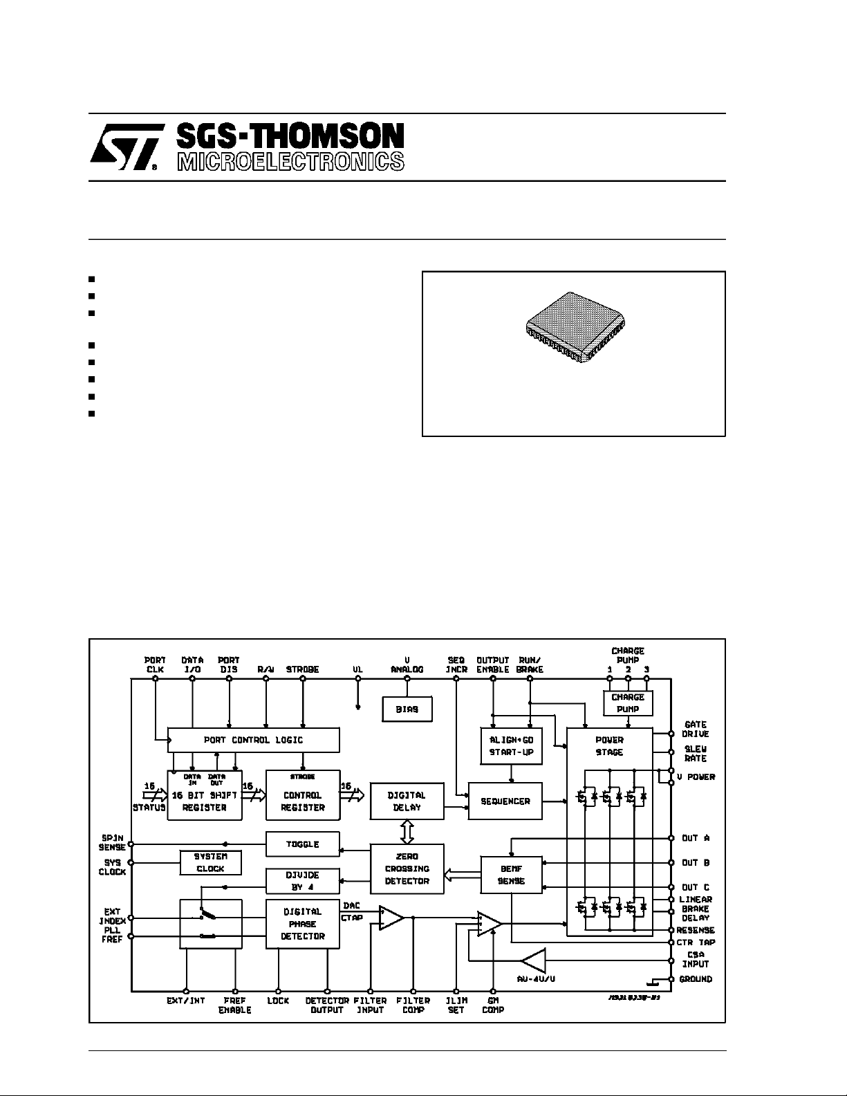
PLCC44
ORDERING NUMBER: L6238
DESCRIPTION
The L6238 is a complete Three-Phase, D.C.
Brushless Spindle Motor Driver system. The device features both the Power and Control Sections and will operate Stand Alone, or can be
used in Higher Power Applications with the addition of an external Linear Driver.
Start-Up can be achieved with the Fully-Integrated Align + GO Algorithm or may be sequenced manually for User-Definedstart-up algo-
BLOCK DIAGRAM
rithms.
A Digital PLL provides high accuracy and the ca-
pability to do Master/Slave Synchronization for
Disk Array configurations.
Programmable functions include commutation
Timing Adjustment and Slew Rate Control for
peakefficiencyand minimum noise.
Protective features include Stuck Rotor\Backward
Rotation Detection and Automatic Thermal Shutdown.
June 1993
This is advanced information on anew product now in development orundergoing evaluation. Details are subject to change without notice.
1/35
L6238
ABSOLUTE MAXIMUMRATINGS
Symbol Parameter Value Unit
BV
dss
V
Power
V
Logic
V
Analog
V
in
I
mdc
I
mpk
P
tot
Ts Storage and Junction Temperature -40 to 150 °C
PIN CONNECTION (Top view)
Output Brakdown Voltage 17 V
MotorSupply Voltage 15 V
LogicSupply Voltage 7 V
Analog Supply Voltage 15 V
InputVoltage -0.3 to 7 V
Peak Motor Current (DC) 3 A
Peak Motor Current (Pulsed: Ton= 5ms, d.c. = 10%) 5 A
Power Dissipation at Tamb = 50°C 2.5 W
THERMAL DATA
Symbol Parameter Value Unit
Thermal Resistance Junction-Pin 7 °C/W
Thermal Resistance Junction-Ambient (Float.) 68 °C/W
Thermal Resistance 34 °C/W
2/35
R
th (j-pin)
R
th (j-amb)
R
th (j-amb)
L6238
GENERALDESCRIPTION
The L6238 is an integrated circuit that will be
used to commutate and speed control a 3-Phase,
8-pole, brushless, DC motor. The primary application is for disk drive spindle motors. This I.C. has
the following features:
No Motor Hall Effect Sensors are required for
commutationor speed control. Timing information is determined from the Bemf voltage of the
undrivenmotor terminal.
On-board Speed Control via a Phase Locked
Loop that accepts a once-per-rev reference
frequency and locks the motor to that frequency. The L6238 can accomodate a wide
range of speeds.
The L6238 achieves Spindle Synchronization
by locking to a once-per-rev reference that is
common to multiple drives. The L6238 has a
multiplexer that enhances the versatility of the
controller. This first multiplexer selects either
internal feedback, (generated by the Bemf of
the motor), or external feedback (embedded
index).
An External P-Channel FET can be connected
to the FET can be connected to the FET
Bridgefor HigherPower Applications.
In this configuration, the internal DMOS drivers
are sequenced in full conduction state and the
external PFET is the linear control element. An
internal inverting buffer from the output of the
OTAcontrolsthe conductionof the EXT PFET.
An internal Virtual Center Tap is used if the
motorcenter tap is not connected.
The motor Current Limit can be set by an externalresistor divider.
A Serial Port is included so that I/O can be
done with a minimum of pins. Key control and
status lines are also bonded out to achieve a
MinimumConfigurationwithout using the Serial
Port.
Programmable Functions include Phase
Switch Timing Optimization for motor efficiency, Speed Lock Threshold, Auto-Start or
mPSupervised Spinup, and output current limitinggain.
Energy Recovery Mode for Head Retraction,
followedby Dynamic Braking Mode.
Logic signals are CMOS Compatible.
Stuck Rotor and Backward Rotationdetection.
Automatic Thermal Shutdown with early warn-
ing bit available in the statusregister
PIN FUNCTIONS
N. Name I/O Function
1 OUTPUT B I/O DMOS Half Bridge Output and Input B for Bemf sensing.
2 SPIN SENSE O Toggless at each Zero Crossing of the Bemf.
3 BRAKE DELAY I Energy Recovery time constant, defined by external R-C to ground.
4R
5 CHARGE PUMP 2 I Negative Terminal of Pump Capacitor.
6, 7,
17, 29,
39, 40
8 CHARGE PUMP 1 I Positive terminal of Pump Capacitor.
9 CHARGE PUMP 3 I Positive terminal of StorageCapacitor.
10 OUTPUT A I/O DMOS Half Bridge Output and Input A for Bemf sensing.
11, 42 V
12 V
13 SER PORT
14 SER DATA R/W I Selects Serial Data Read or Write Function.
15 SER STROBE I Dtat Strobe Input.
16 SER PORT CLK I Clock for Serial Data Control.
18 SER DATA I/O I/O Data stream Input/Output for Control/Status Registers.
19 EXT/INT I Selects thr Internal BEMF ZeroCrossing or an External Source as Feedback
20 FREF ENABLE I A zero on this pin passes thePLL Fref signal to the Freq/phase detector.
21 LINEAR I This input should be grounded or left unconnected.
22 OUTPUT
sense
GROUND I Ground terminals.
power
analog
DISABLE
ENABLE
O Outputs A+B connections for the Motor Current Sense Resistor to ground
I Supplies the voltage for the Power Section.
I 12V supply.
I Input for tri-stating the serial port.
Frequency for te PLL.
I Tristates Power Output Stage when a logic zero.
3/35
L6238
PIN FUNCTIONS (continued)
N. Name I/O Function
23 RUN/BRAKE I Rising edge will initiate start-up. A Brakingrountine is started when this input is
24 SEQINCREMENT I A low to high transition on this pin increments the Output State Sequencer.
25 SYSTEM CLK I Clock Frequency for the system timer/counters.
26 EXT INDEX I External Source of Feedback for the PLL.
27 PLL Fref I Reference Frequency for the PLL.
28 LOCK O High when the PLL is phase_locked.
30 Vlogic I Logic power supply.
31 DETECTOR OUT O Output of Frequency/Phase Detector.
32 FILTER IN I Filter Input.
33 FILTER COMP O Filter output and compensation.
34 CSA INPUT I Input to the Current Sense Amplifier.
35 Rsense O Output C connection for the Motor Current Sense Resistor to ground.
36 OUTPUT C I/O DMOS HalfBridge Output and Input C for Bemf sensing.
37 gm COMP I A series RC network to ground that defines the compensation of the
38 GATE DRIVE I/O Drives the Gate of the External P Channel DMOS Driver for Higher Power
41 I LIMIT SET I A voltage applied to this pin, in conjunction with the value for the external
43 CENTER TAP I Motor Center Tap used for differentialBEMF sensing. If the center tap of the
44 SLEW RATE I A resistor connected to this pin sets the Voltage Slew Rate of the Output
brought low.
Transconductance Loop.
Applications. This pin must be grounded if an external driver is not used.
Motor Current Sensing resistor, defines the maximum Motor Current.
Motor is not brought out, a virtual center tap is integrated and available at this
pin.
Drivers.
ELECTRICAL CHARACTERISTICS (Refer to thetest circuit,unless otherwise specified.)
Symbol Parameter Test Condition Min. Typ. Max. Unit
POWER SECTION
V
Power
R
DS(on)
I
o(leak)
V
F
dVo/dt Output Slew Rate R
I
m(max)
I
gt
T
sd
T
hys
T
ew
I
snsin
G
V
Z
inCT
Motor Supply 10.5 12 13.5 V
Output ON Resistance Tj=25°C
T
= 125°C
j
0.25 0.33
0.50
Output Leakage Current 1 mA
Body Diode Forward Drop Im= 2.0A 1.5 V
= 100KΩ 0.30 V/µs
slew
Motor Current Limit (Note 1) Rs= 0.33Ω
I
Gate Drive for Ext. Power
DMOS
lim
I
lim
I
LIMSET
I
lim
Gain = 0
Gain = 1
=5V
Gain = 0
TBD
TBD
0.75
0.38
TBD
TBD
5mA
V33 = 0V, V38 = 5V
Shut Down Temperature 150 180 °C
Recovery Temperature
30 °C
Hysteresis
Early Warning Temperature Tsd-25 °C
Current Sense Amp Input Bias
10 µA
Current
Current Sense Amp Voltage
3.8 4 4.2 V/V
Gain
Center Tap Input Impedance 30 KΩ
Ω
Ω
A/V
A/V
4/35
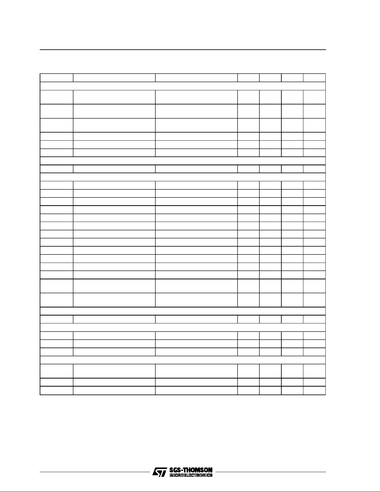
ELECTRICAL CHARACTERISTICS (Continued)
Symbol Parameter Test Condition Min. Typ. Max. Unit
LOGIC SECTION
V
inH
V
inL
I
inH
I
inL
V
outL
V
outH
F
sys
t
on
t
off
SEQUENCE INCREMENT
t
seq
SERIAL PORT TIMINGNote: C
Fshift Clock Frequency 2 TBD MHz
t
os
t
settle
t
strobe
t
wait
t
ds
t
dh
t
sd
tcd Clock to Data Prop. Delay (*) 100 ns
t
sd
t
tsd
t
wrs
t
scr
t
csw
PHASE LOCK LOOP SECTION
T
phse
BRAKE DELAY SECTION
V
chrg
I
out3
V
Thres
CHARGE PUMP
V
out9
V
leak
F
cp
(*) These parameters are a function of C
Input Voltage TBD
TBD
Input Current
1 µA
–1
Output Voltage V
= 2mA
sink
V
= 2mA 4.5
source
0.5 V
System Clock Frequency 8 12 MHz
Clock ON Time 20 ns
Clock OFF Time 20 ns
Time Between Rising Edges 1 µs
(data I/O) = 50pF;
load
Operating Set-up Time 50 ns
Enabling Settling Time 50 ns
Strobe Pulse Width 40 ns
Disable Wait Time 40 ns
Data Setup Time 100 ns
Data Hold Time 10 ns
Strobe to Data Prop. Delay (*) 100 ns
Data I/O Activation Delay (*) 100 ns
Data I/O Tri State Delay 80 ns
Write to Read Set-up Time 50 ns
Strobe to Clock Time
50 ns
(Read Mode)
Clock toStrobe Time
50 ns
(Write Mode)
Static Phase Error 20 µs
Capacitor Charge Voltage RT = 50K TBD 9.5 TBD V
Source Current 0.5 mA
Delay Timer Low Trip Threshold TBD 1.8 TBD V
Storage Capacitor Output
20 V
Voltage
Blocking Diode Leakage Current 10 µA
Charge Pump Frequency 300 KHz
.
load
L6238
V
V
mA
V
5/35
L6238
FUNCTIONAL DESCRIPTION
1.0 INTRODUCTION
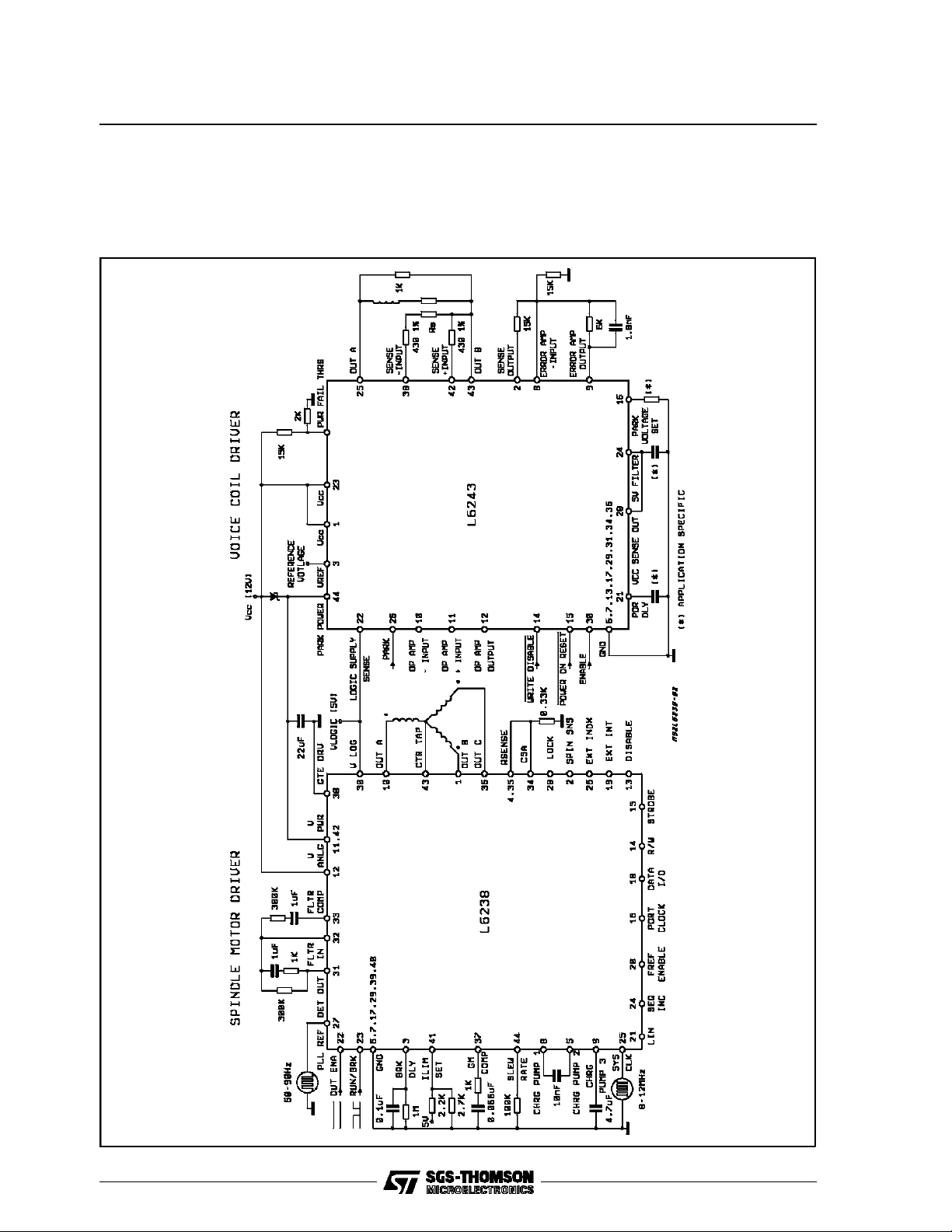
1.1 Typical Application
In a typical application, the L6238 will operate in
Figure1: StandAlone Configuration
conjunction with the L6243 Voice Coil Driver as
shown in Fig. 1. This configuration requires a
minimum amount of external components while
providingcompletestand-aloneoperation.
6/35
L6238
1.2 Input Default States
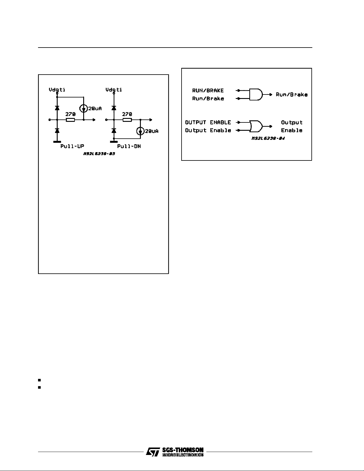
Figure2: InputStructures
FUNCTION CONFIGURATION
PORT DIS
STROBE
PORT CLK
R/W
DATA I/O
EXT/INT
FREF ENABLE
LIN
OUTPUT ENABLE
RUN/BRAKE
SEQ INCR
SYS CLOCK
EXT INDEX
PLL FREF
PULL-UP
PULL-DOWN
PULL-UP
PULL-UP
PULL-UP
PULL-DOWN
PULL-DOWN
PULL-DOWN
PULL-DOWN
PULL-UP
PULL-DOWN
PULL-UP
PULL-UP
PULL-UP
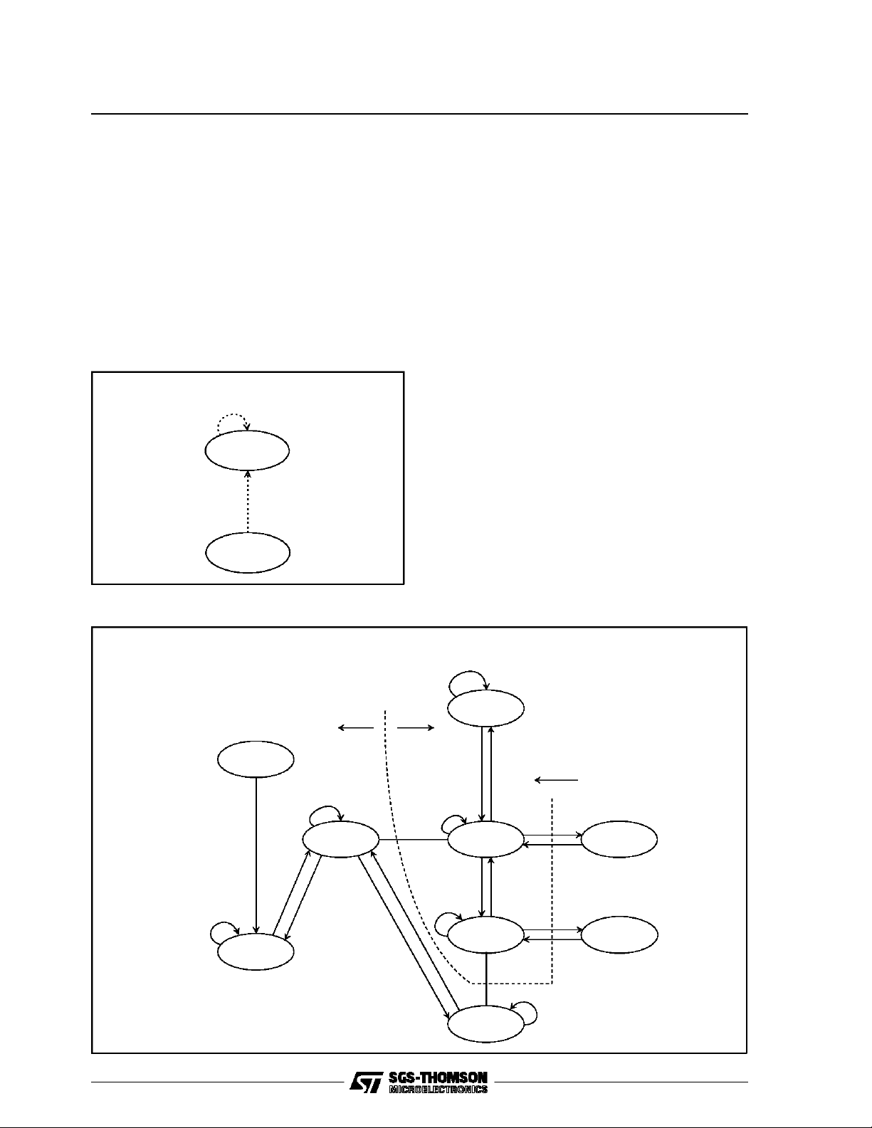
Figure 2 depicts the two possible input structures
for the logic inputs. If a particular pin is not used
in an application, it may either be connected to
ground or VLOGIC as required, or simply left unconnected. If no connection is made, the pin is
either pulled high or low by internal constant current generatorsas shown
A listing of the logic inputs is shown with the correspondingdefaultstate.
1.3 Naming Convention
In order to differentiatebetweenthe various types
of control and status signals, the followingnaming
conventionisused.
BOLDCAPITALS - Devicepins.
Italics -
Serialport controland status signals.
Threeinput signals form a special case. Referring
to figure 3, the RUN/BRAKE input pin and the
Run/Brake
tion, while OUTPUT ENABLE and
control signal form a logical AND func-
Output Enable
form an OR function. The outputs signal names,
in Bold Lowercase labeled Run/Brakeand Out-
put Enable will be used when referring to these
Figure3: Input Logic
signals. Although not shown, SEQUENCE INCREMENT and
Sequence Increment
also form
an OR function, with the resultant output signal
calledSequenceIncrement.
1.4 Modes of Operation
Thereare 5 basic modes of operation.
1) Tristate
When Output Enable is low, the output power
driversare tristated.
2) Start-Up
With Output Enable high, bringing Run/Brake
from a low to a high will energize the motor and
the system will be driven by the Fully-Integrated
StartUp Algorithm. A user-defined Start-Up Algorithm, under control of a MicroProcessor, can be
achieved via a serial port and/or external control
pins.
3) Run
Identified by the Lock signal, Run mode is
achievedwhen the motor speed (controlledby the
Internal PLL) reaches the nominal speed within a
predefinedphaseerror.
4) Park
When Run/Brake is brought low, energy to park
the heads may be derived fromthe rectifiedBemf.
The energy recovery time is a function of the
Brake Delay Time Constant. In this state, the quiescent current of the device is minimized (sleep
mode).
5) Brake
After the Energy Recovery Time-Out, the device
is in Brake, with all lower Drivers in full conduction.
Duringa power down, the Park Mode is triggered,
followedby a DynamicBrake.
There are two mutually exclusive conditions
which may be present during the Tristate Mode
(wake up):
7/35
L6238
a)the spindle is stopped.
b)the system is still running at a speed that
allows for resynchronization.
In order to minimize the ramp up time, the microcontrollerhas the possibilityto:
check the SPIN SENSE pin, (which toggles at
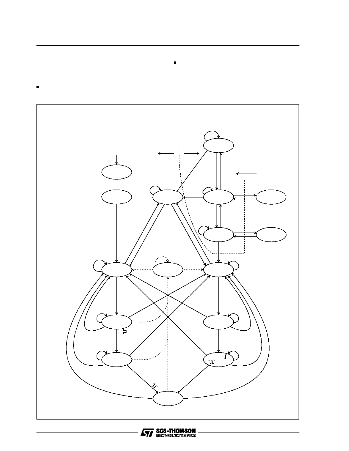
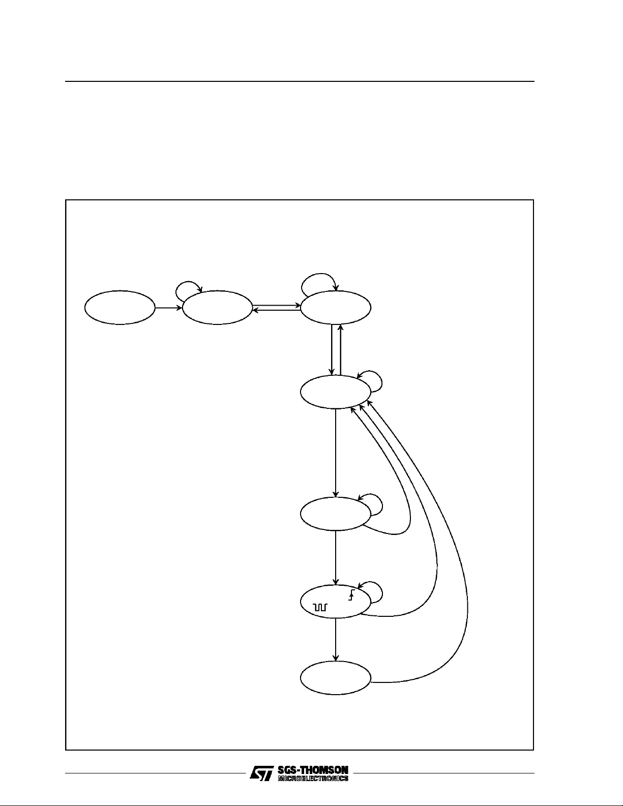
Figure4: StateDiagram
From Anywh er e
Auto/Ext = 0
Hold for
”Align & Go”
Power
on
Reset
1
=
k
r
0
B
=
n
a
u
n
R
E
t
u
O
0
=
a
n
E
t
n
u
E
t
O
u
O
N
Hold
for
”Resync”
0
=
0
a
=
a
n
E
t
u
O
c
Z
o
Star t
”Resync”
RunB r k = 0
OutEna = 0
0
=
e
k
a
r
B
n
u
R
R
StrRtr = 0
&
1
=
e
k
a
r
B
n
u
the Bemf zero crossing frequency)
enable the power to the motor based on the
previousinformation. Otherwise the uP may issue a Brake command, followed by the startup procedure after the motor has stopped spinning.
Auto St ar t-up
Enabled Disabled
RunBr k = 1
OutEna = 0
Hold & wai t
for d ecisio n
O
u
O
t
E
u
n
t
E
a
n
=
a
0
=
1
OutEna = 1
&
RunBr k = 1
Stuck
Rotor
(hold)
RunB r k = 0
OutEna = 0
SeqInc = X
RunBr k = 1
OutEna = 1
”A lign & Go”
”A lign & Go”
Brake
W/Mask
RunBrk = 1
Tri -sta t e
W/Mask
OutEna = 1
Run
W/Mask
RunBrk = 0
Hold fo r
RunBrk = 1
[Align to Phase # 1]
Star t
Action acro ss
line increments
sequ enc er
RunBrk = 0
SeqInc = 0
SeqInc = 1
OutEna = 0
SeqInc = 0
SeqIn c = 1
OutEna = 1
RunB r k = 0
O
O
u
O
t
E
u
n
t
E
n
a
=
0
A
l
i
g
n
Tri - s t ate
W/Mask
RunB r k = 1
OutEna = 0
Run
Wo/Mask
RunBrk = 1
OutEna =1
&
u
t
E
n
a
=
a
0
=
0
=
0
8/35
o
N
c
Z
Resyn c = 1
Release
min mask
(Get 1st Zc)
Zc Reset=
StrRtr = 0
(
G
e
Z
t
c
R
e
Align = 1
[Align to
G
Phase # 3]
o
=
Align =
Seqncr.
2
n
d
Z
s
e
c
t
)
=
Mono = 0
StkRtr = 0
Run
1
=
o
G
0
L6238
2.0 STATE DIAGRAMS
2.1 State Diagram
Figure 4 is a complete State Diagram of the controller depicting the operational flow as a function
of the control pins and motor status. The flow can
be separatedintofour distinct operations.
Figure5: Align+Go
RunBrk = 1
OutEna = 0
Power
on
Rese t
Hold
for
”Resync”
RunBrk = 0
RunBrk = 1
2.2 Align + Go
Figure 5 represent the normal flow that will
achieve a spin-up and phase lock of the spindle
motor. Upon power up, the controller first checks
to determine if the motor is still spinning. This
”Hold For Resync” decision block will be discussedlater.
Hol d & wa i t
for decisio n
OutEna = 1
OutEna = 0
Hold fo r
”Align & Go”
OutEna = 0
&
Run Br k = 0
RunBrk = 1
[Align to Phase # 1]
Start
”Align & Go”
Align = 1
[Align to
Align =
Seqncr.
Go = 1
Run
O
u
O
t
u
O
u
Phase # 3]
E
t
n
E
a
n
t
E
n
A
=
a
0
=
0
a
=
0
l
i
g
n
=
0
G
o
=
0
9/35
L6238
Assuming the motor is stationary, with Output
Enable high and Run/Brake low, the controlleris
in the ”Hold for Align & GO” state. When
Run/Brake is brought high, the motor is in align
mode with Phase 1 active (Output A high and
Output B low).
Align is
time-out (user-programmable), the
high and the sequencer double increments the
outputs to Phase 3 (Output B high and Output C
low). After the next time-out, the controller enters
the Go mode, with the sequencer automatically
incrementing the output phase upon detection of
the motor’s Bemf.
Never command an Align & Go unless a reference signal is present at PLL FREF, since this
is the signal that determinesthe length of time
that phase 1 remains active.
If Run/Brake is brought low, (or if the 5V supply
is removed) the controller will revert to ”Hold for
Align & GO” and the serial port will be reinitialized. In order to prevent an erroneous restart condition, it is necessary that Run/Brake be held low
until the motor has completely stopped. Once the
motor has stopped, Run/Brake may be brought
high for a completeAlign & Go Start-Up routine.
a zero. After the align
Align
bit goes
2.3 Resynchronization
If power is momentarily lost, the sequencer can
automatically resynchronize to the monitored
Bemf. This resychronization can either occur
wheneverOutput Enable is first brought low then
high or if the Logic Supply is momentarilylost.
Referring to figure 6, the ”Hold for Resync” state
is entered upon POR (Power On Reset) or whenever Output Enable is brought low. The controller leaves this state and enters ”Start Resync”
when Output Enable is high.
If zero crossings are detected,the sequencer will
automatically lock on to the proper phase and
bringthe motor speed up to PhaseLock.
This resynchronization will take effect with the
motor speed running as low as typically 30% of
it’snominal value.
Never command an Align & Go while the motor is spinning. Always initiate a resync first
or initiate brake mode and allow the motor to
spin down.
Figure6: Resync.
Power
on
Reset
1
=
k
r
0
B
=
n
a
u
n
R
E
t
u
O
0
=
a
n
E
t
n
u
E
t
O
u
O
N
N
a
o
o
0
=
O
Z
Z
a
n
E
t
u
c
c
Hold
”Resync”
0
=
Start
”Resync”
Resync=1
Release
min mask
for
OutEna=1
Zc Reset =
(Get 1st Zc)
10/35
Run
(Get 2nd Zc)
Zc Reset =
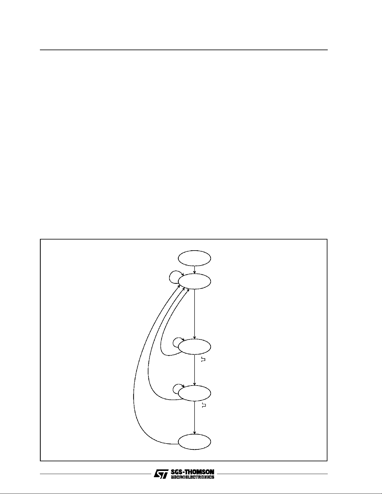
2.4 Stuck Rotor/Monotonicity
Refer to figure 7. In order to alert the microprocessor of fault conditions, two bits are available in
the Serial Port’s StatusRegister.
1. Stuck Rotor
If the controller enters the Go mode after the Double Align, Bemf must be detected within 419ms
when using a system clock frequency of 10MHz.
If this condition is not met, the outputs will be tristated and set this bit to a zero. The controller enters the ”Stuck RotorHold” state.
Figure7: StuckRotor/Monotonicity.
OutEna = 1
&
RunB rk = 1
Stuck
Rotor
(hol d)
Mono = 0
StkRtr = 0
Run
L6238
2. Mono
When the motor spins up normally, the resultant
S P IN SENSE pulses rise in frequency in a
monotonic pattern. Any fault condition that would
cause a rapid decrease in the SPIN SENSE frequency would be detected by internal counters
setting the
MONO
condition
2.5 External Sequencing
Although the user-defined Start-Up Algorithm is
flexible and will consistently spin up a motor with
minimum external interaction, the possibility exists where certain applications might require complete microprocessorcontrolof start-up.
The L6238 offers this capability via the SE-
QUENCE INCREMENT input. Referring to figure
9, with Output Enable and Run/Brake low, the
controller is in the ”Hold and Wait for Decision”
state. If the SEQUENCE INCREMENT pin is
brought high during this state, the Auto StartUp
Algorithm is disabled and the sequencer can be
controlledexternally.
When Output Enable and Run/Brake are
broughthigh, the sequencer is incremented every
time that the SEQUENCER INCREMENT pin is
first brought low and then high. During the time
that this pin is high, all Bemf information is
bit low and forcing a Brake
Figure8: Ext. Sequence.
1
=
k
r
B
0
n
=
u
a
R
n
E
t
u
O
”Resync”
Power
on
Reset
Hold
for
e
k
a
r
B
n
u
R
OutEna = 0
&
RunBrk = 0
Hold & wait
for decision
0
=
1
=
e
k
a
r
B
n
u
R
Auto Start-up
Enabled Disabled
RunBrk = 1
OutEna =0
O
u
t
O
E
u
n
t
a
E
=
n
a
=
RunBrk = 1
0
OutEna = 1
1
RunBrk = 0
OutEna =0
SeqInc = X
W/Mask
RunBrk = 1
Tri-st ate
W/Mask
W/Mask
Hold for
”Align & Go”
Brake
OutEna = 1
Run
RunBrk = 0
Action across
line incr ement s
sequencer
RunBrk = 0
SeqInc = 0
SeqInc = 1
OutEna = 0
SeqInc = 0
SeqInc = 1
OutEna = 1
&
RunBrk = 0
Tri-state
W/Mask
RunBrk = 1
OutEna = 0
Run
Wo/Mask
RunBrk = 1
OutEna = 1
11/35

L6238
maskedout, and when it is low, the Bemf information can be detected normally. When the motor
has reached a predetermined speed, the SEQUENCE INCREMENT pin can be left low and
the L6238 Motor Control logic will take over and
automaticallybring the motor into Phase Lock.
3,0 START-UP ALGORITHMS
3.1 Spin-Up Operation
The spin operation can be separatedinto 3 parts:
1) Open Loop Start-Up - The object is to create
motion in the desired direction so that the Bemf
voltagesat the 3 motor terminals can provide reliable information enabling a transition to closed
loop operation.
2) Closed Loop Start-Up - The Bemf voltage
zerocrossings provide timing information so that
the motor can be accelerated to steady state
speed.
3) Steady-State Operation - The Bemf voltage
zero-crossingsprovide timing information for precision speed control.
The L6238 contains features that offer flexible
control over the start-up procedure. Either the on-
Figure9: AutoStart Profile
board Auto-Start Algorithm can be used to control
the start-up sequence or more sophisticated extemal start-up algorithms can be developed using
the Serial Port and key control/sense functions
broughtout to pins.
3.2 Auto-Start Algorithm
The Serial Port Control Bit
Auto/Ext
(Refer to Table 2), controls the start-up mode. The power up
default state is a logic high which selects the
AutoStart Mode. When Run/Brake is low, the
L6238 is in brake mode, and the Auto-Start Algorithm is reset. In the brake mode, all of the lower
DMOS drivers are ON, and the upper drivers are
OFF.
Note that Run/Brake should be brought low for a
period exceeding the value selectedfor the brake
delay time in order to initialize the brake delay circuit.
The Auto-Start Algorithm is based on an Align &
Goapproach and can be visualizedby referring to
Figure 9. Shown are the Output Enable and
Run/Brake control signals,sequencer output with
Align
the resultant output phases, and the
and Go
status bits. The times labeled Tl and T2 are two
T
<1> T
asd
0
0
1
1
Note: PLL ReferenceFrequency = 90Hz
12/35
<0> Ta=T
asd
0
1
0
1
0.178 s
0.356 s
0.533 s
0.711 s
1
T
2
0.533 s
1.067 s
1.600 s
2.133 s
T
g
0.711 s
1.422 s
2.133 s
2.844 s

L6238
delays that are 25% and 7S% respectively of the
Delay
total delay selected by the Auto-Start
trol Bits. The times labled T1 andT2 are the times
associatedwimthe
cal delays associated with these times for a PLL
referencefrequencyof 90Hz are shownin the figure.
Referring to figure 9, the following is the sequence of events during Auto-Start:
AlignmentPhase
- Output Stage is energized to phase 1 with
OUTPUT A high and OUTPUT B low for T
seconds.
- The intemal sequencer double increments the
output stage to Phase 3 for T2 seconds. If
phases 1 or 3 are high torque states, the motor should become aligned.
- During the alignment phase, the SEQ INCRE-
MENT signalis ignored.
Go Phase
- The internal sequencer double increments the
output stage to State 5, whichshouldproduce
torquein the desired direction.
- with SEQ INCREMENT held low, the se-
quencer is now controlled by the Bemf zero
crossings, and the motor should ramp up to
speed.
If backwardrotation is detected, a status bit in the
serial port will be set, and the L6238 will revert to
the brake mode.
- If a stuck rotor condition exists, the
tor
Status bit is flagged, but no action is
taken. If though during a stuckrotor condition,
the time outdue to the backwardsrotationoccurs, the L6238 will revert back to the brake
mode.
Align
and Go status bits. Typi-
Con-
Stuck Ro-
or cycle through the states at any desired rate.
When held high, it inhibits the BEMF zero
crossings from incrementing the internal sequencer.
SPIN SENSE This output is low until the first
detected Bemf zero crossing occurs. It then
toggles at each successive zero crossing. This
signal serves as a motion detector and gives
useful timing information as well.
LOCK A high denotes that the phase error between the PLL reference and the feedbacksignals is within the programmed threshold. This
signalis updated once per revolution.
Seq Reset
stageto the first state.
3.4 Start Up Approaches
Align & Go Approach The Align & Go approach
provides a very time efficient algorithm by energizing the coils to align the rotor and stator to a
known phase. This approach can be achieved via
Seq Reset,
the
SPIN SENSE can be monitored to assure that
motion occurred. Once ample time is given for
alignment to occur, SEQ INCR can be double incremented, and the SPIN SENSE pin can be
monitored to detect motion. When SEQ INCR is
pulled low, control is transferredto the internal sequencer, and the L6238 finishes the spinup operation. If no motion is detected, SEQ INCR can
be incremented to a different phase and the process can be repeated. The alignment phase may
cause backward rotation, which on the average
will be greater than the StepperMotorapproach.
This bit is used to reset the output
or by sequencing SEQ INCR.
3.3 Externally Controlled Start-Up Algorithms
Enhanced Start-Up Algorithms can be achieved
by using a uProcessortointeractwith the L6238’s
control and status signals. The uProcessor needs
to be heavily involved during OpenLoop Start-Up.
The L6238 has the ability to transition to Closed
Loop Start-Up at very low speeds, reducing the
uProcessor task to monitoring status rather than
real time interaction. Thus, it is a perfect application for an existinguProcessor.
To allow control via an external means, the
Auto/Ext
low. This disables the internal Auto-Start Algorithm. The following control and status signals allow for very flexible algorithmdevelopment:
Control Bit in the Serial Port must be set
SEQ_INCR A low to high transition at this input
isused toincrementthe stateof the power output stage. It is useful during start-up, because
the µProcessor can cycle to any desired state,
The Auto-Start algorithm described earlier is an
Align & Go approach. The main advantages of
the integrated Auto-Startare that the uP is not involved real-time, and there are a minimum of interface pins required to the spindle control system.
Stepper Motor Approach This approach minimizes backward rotation by sequencing SEQ
INCR at an initial rate that the rotor can follow.
Thus, it is driven in a similar fashion to a stepper
motor. The rate is continuallyincreaseduntil the
Bemf voltage is large enough to reliably use the
zero-crossings for commutation timing. SEQ
INCR is held low, causing control to be passed to
the L6238’s internal sequencer as in the Align &
Go approach.
The Stepper Motor approach takes longer than
the Align & Go approach because the initial commutation frequency and subsequent ramp rate
13/35

L6238
Figure10: PhaseDetectorState Diagram.
must be low enough so that the motor can follow
without slipping. This implies that to have a reliable algorithm, the initial frequencyand ramp rate
must be chosen for the worst case motor under
worst case conditions.
4.0 DIGITAL PLL MOTOR SPEEDCONTROL
4.1 Phase Detector
The internal Phase/Frequency Detector of the
PLL has two inputs:
- reference input (Fref)
- feedbackinput (Fmtr)
The feedback Input is multiplexed between the in-
ternal Bemf Zero CrossingDetector and an externallyprovidedsync pulse (EXT INDEX)
14/35
Shown in figure 10 is the classical state diagram
for a phase detector along with waveform examples.
Positive phase is defined as when the reference
falling edge occurs before the falling edge of
Fmotor and the motor speed must be increased.
Negative phase is just the opposite, requiring a
slowingof the motor speed.
As an example, the top four waveforms in figure
10 represent a positive phase condition. In this
casethe ”up” signal would go low since the reference signal went low before the appearance of a
negative transition of fmotor. The falling edge of
fmotor causes the ”up” signal to revert back to a
high. The period while the ”up” signal is in a low
state is a functionof the phase difference.

Figure11: LogicBlock Diagram.
L6238
4.2 Counter Section
Figure 11 is a block diagram of the counter section of the PLL along with the phase detector.
The phase detectorprovides up and down signals
that are used to control the direction and counting
period of two 8 bit counters. Two counters are
used to provide both coarse and fine phase error
information.The coarse counter operates to bring
the phase error into a finite window, while the fine
counter with it’s higher resolution controls the
phasejitter to typically 5µs.
As an example, during a positive phase measurement, the counters are reset to 10000000 which
is the middle of their measurement range corresponding to zero degrees phase error. The falling
edge of Fref, in conjunction with the ”up” signal,
causes the fine counter to then start counting up.
The coarse counter is inhibited by the fine counter
until the fine counter has reached it’s maximum
count. The falling edge of Fmtr causes the counters to stop counting and the bits in the fine and
course counters are then latched into their respective latches. The counters are then reset to
10000000 in anticipation of the next phase measurement.
The operation of the counter section during spinup and phase lock can be described in three
phases:
1) Initial Spin-Up - At start-up the PLL will inher-
entlybring the motorspeed ”in line” with the reference frequency.The phase detector is initialized
atpower up to force the countersto start counting
up.
Since there will be many more Fref. vs Fmtr falling edges at start-up, the width of the ”up” pulse
will be wide. The fine counter will reach it’s maximum count and send an enable pulse to the
coarse counter causing it to start counting. After
127 counts, the coarse counter also reaches it’s
maximum count. At the end of the ”up” pulse, it’s
rising edge loads the outputs of the Coarse and
Fine counters into corresponding latches. Thus
the latches are updated once-per-rev with a binary number that corresponds to the measured
phase error. This count will be converted via a
Digital to Analog Convertors (DAC) into a speed
Command Voltage, which at start-up will be the
maximumas set by the ILIM SET voltage.
2) Overshoot - As the motor speed increases
close to the reference, the coarse counter comes
out of complianceand decreasesit’s count as the
phase difference becomes smaller. The fine
counter then takes over when the phase is in a
certain range. A certain amount of phase overshoot will take place as the motor passes though
zero phase difference due to the closed loop system response characteristics.
This will cause the counters to count down to
”slow” the motor down until the phase difference
isminimal.
15/35

L6238
Figure12: Coarseand Fine DAC’s.
3) Phase Lock - After a brief settling time, typically 1-2 seconds after spin-up, the counters will
alternately count up and down as required to
maintain the phase difference to be as close to
minimum as possible. The counter outputs at this
time should be ”hovering” around10000000.
The outputs of the two DACs are sent to latches
that store the digital representation of the meas-
be used to command the output driver’s current.
In figure 12, the two 8-bit digital error signals are
used to switch in 256 possible voltages derived
from a precision Band-Gap reference. The same
resistor ladder string is used for the Coarse and
Fine DACs. The outputs of the DACS are then
sent to buffer stages and added together via a
summingamplifier.
ured phase error. This information is then bussed
to the DACs.
4.4 Transfer Functions
Figure 13 represent the Output Voltage vs Phase
4.3 Coarse/FineDACs
Two DACs are used to convert the digital phase
error information into an analog voltage that can
Error for the Coarse and Fine DACs depicting the
resolutionthatis achievable.
Table 2 shows examples of the resolution of both
Table 2
Fsystem
Clock
8MHz 15.6KHz 64.1µs 16.3ms 1.0MHz 1.0µs 255µs
10MHz 19.5KHz 51.3µs 13.1ms 1.25MHz 800ns 204µs
12MHz 23.4KHz 42.7µs 10.9ms 1.5MHz 667ns 170µs
16/35
Fcoarse
Phase LSB
Coarse
(Range)
Coarse
Ffine
Phase LSB
Fine
(Range)
Fine

Figure13: Coarse/FineDAC’sOutputGraphs.
L6238
DACs as a function of the system clock repetition
rate. Fcoarse is the system clock divided by 512,
while Ffine divides the clock by 8. This gives for
example, Coarse and Fine LSB’s of 51.3us and
800ns respectively for a system clock repetition
rate of 10MHz. Thereforethe best phase jitter that
could be achieved as a function of the counter
resolution is 800ns. The dynamic range of each
counteris also shown in the table.
It can be seen that the ratio of Fine to Coarse
counts is 64. The summing amplifler divides the
Fine DAC buffer output voltage by a factor of 16.
Therefore there is a 4:1 ratio of Fine to Coarse
gain.
This results in a Speed Control Loop that is fairly
easy to compensate with excellent transient response.
The output of the PLL Detector is fed to a general purpose. filter amplifier that is used to compensate the Speed Control Loop. The filter amplifier
output stage has been carefully designed to limit
the compliance voltage to a value that tracks the
Ilim Set voltage, thus limiting the amount of overshoot and enhancing the transient response of
the loop.
4.5 PLL DetectorOutput
Figure 14 is a graph of the typical DETECTOR
OUTPUT voltage as a function of the detected
phase difference as measured on production material. The change of the gain slope is apparent
around the zero phase difference point. With the
spindle motor at phase lock, the DETECTOR
OUTPUT voltage is typically 2.0, equivalent to the
internalVirtual Ground level.
Figure14: V
Outputvs Phase Error.
detector
17/35

L6238
5.O MOTOR DRIVER
5.1 Output Stage
The output stage forms a 3-phase, full wave
bridge consisting of six Power DMOS FETs capable of 2.5 amps. Higher output currents are allowed for brief periods. Output Power exceeding
the stand-alone power dissipation capabilities of
the L6238 can be increased with the addition of
an externalP-FET.
Table 3 is a reference diagram that lists the parameters associated with 8-pole motors operating
at 3600 and 5400 RPM.
Figure 15 represents the waveforms associated
with the output stage. The upper portion of figure 15 shows the flow of current in the motor
windings for each of the 24 phase increments. A
rotational degree index is shown as a reference
along with a base line to indicate the occurrence
of a zero crossing. The 3 output waveforms are
actual digitally reproduced voltage signals as
measuredon samples.
A typical sequence starts when the outputsswitch
states.Referring to figure 15, during phase 1, output A goes high, while output B is low. During this
Table 3.
phase, output C is floating, and the Bemf is monitored.The outputs remain in this state for 60 electrical degrees as indicated by the first set of
dashed lines. After this period the outputswitches
to phase 2 with output A high and C low with the
Bemfamplifier monitoringoutput B.
In order to preventcommutation current noise being detected as a false zero crossing, a masking
circuit automatically blanks out all incoming signals as soon as a zero crossing is detected.
When the next commutation occurs an internal
counter starts counting down to set the time that
the masking pulse remains The counter is initially
loaded with a number that is equal to period that
is always 25% of the previousphase period or 15
electrical degrees. This time-out of the masking
pulse shown for reference at the bottom of figure
16. Thus the actual masking period is the total of
the time from the detected zero crossing to the
commutation, plus 25% of the previous period.
The mask pulse operation is further discussed in
section5.6, Slew Rate Control.
Afterthe masking period, the Bemf voltage at output B is monitored for a zero crossing. Upon detectionof the crossing the output is sequenced after 30 electrical degrees insuring maximum
18/35
Rotational Speed 3600 rpm 5400 rpm
Rotational Freq. 60Hz 90Hz
Rotational Period 16.667 ms 11.111 ms
Electrical Period 4.167 ms 2.778 ms
Phase Period 694.5 µs 463.0 µs

Figure15: BrakeDelay.
L6238
19/35

L6238
torque. The spin sense waveform at the bottomof
the figure indicates that this output signal toggles
with each zero crossing.
5.2 Brake Delay
When Run/Brake is brought low, a brake is initiated. Referring to figure 16, SWI is opened and
the brake delay capacitor, C
dischargetowards ground via R
, is allowed to
brake
. At the same
brake
time, switches SW2 through SW7 bring the gates
of the output FETs to ground halting conduction,
causing the motor to coast. While the motor is
coasting, the Bemf is used to park the heads.
When C
reaches a voltage that is below the
brake
turn ON threshold of Q I, Switches SW8, 9 and 10
bring the gates of the lower drivers to V
brake
potential. This enables the lower FETs causing a
braking action. This braking action also occurs if
the logic supply is lost. The analog supply is not
Figure16: BrakeDelay.
monitored in the L6238 since the L6243 already
monitorsthis voltage and initiates a Park function
when this supply drops to apredeterminedlevel.
If multiple logic supplies are used in the application, all logic signals to the L6238 including the
reference and clock signals should be buffered
with gates powered by the same supply as the
L6238 in order to prevent erroneous operation.
This would occur, for example, if the5V supply to
the controller were lost while5V were still present
atone of the logic pins. This would partiallypower
the chip, causing unpredictableoperation.
5.3 Charge Pump
The charge pump circuitry is used as a meansof
doubling the analog supply voltage in order to allow the upper N-channel DMOS transistors to be
driven like P-channel devices. The energy stored
in the reservoir capacitor is also used to drive the
20/35

Figure17: ChargePump Circuit.
L6238
lower drivers in a brake mode if the analog supply
islost.
Figure 17 is a simplified schematic of the charge
pump circuitry. A capacitor, C
, is used to re-
pump
trieve energy from the analog supply and then
”pumps” it into the storage capacitor, C
resvr
. An internal 300kHz oscillator first turns ON Q2 to
quickly charge C
to approximately the rail
pump
voltage. The oscillator then turns ON Ql while
turning OFF Q2. Since the bottom plate of C
is now effectively at the rail potential, C
resvr
pump
is
chargedto ~twice the rail voltage via D2. A zener
referenced series-pass regulator supplies a voltage,V
, duringbrake mode.
brake
5.4 Output CurrentControl
The output current is controlledin a linear fashion
via a transconductance loop. Referring to figure
18, the sourcing FET of one phase is forced into
full conduction by connecting the gate to V
pump
while the sinking transistor of an appropriate
phase operates as a transconductance element.
To understand the current control loop, it will be
assumed that Q2 in figure 18 is enabled via SW2
by the sequencer.
During a run condition, the current in Q2 is monitored by a resistor R
connectedto the R
4
sense
input. The resulting voltage that appears across R4
isamplified by a factorof four by A3and is sent to
A2 where it is compared to the PLL error signal.
A2 provides sufficient drive to Q2 in order to
maintain the motor speed at the proper level as
commandedby the PLL.
During initial start-up, the error signal from the
output of the PLL Phase/Frequency Detector will
be at compliancein order to quickly bring the motor up to correct speed. The motor current during
this condition can be safely limited to a predetermined value by applying a voltage to the ILIM
SET input.
The voltage at this input is buffered by A1 and
sent to multiplexer, SWl. The output voltage of the
multiplexer,
Vclmp, is
used to control the maximum non-inverting input voltage for amplifier A2.
This multiplexer also receives a voltagethat is 1/2
the ILIM SET value via a resistor divider connected to the buffer. Control bit
llim Gain
mines which voltage is available at the output of
the multiplexer and allows a 2:1 change in the
output current limit under software control.
For example, if the
,
high, and 3.3V were applied to the ILIM SET input, then V
clmp
Ilim Gain
control bit is set
would equal 1.65V. Since A3 has
a voltagegain of 4, this would translate to a maximum sensed voltage at the R
input equal to
sense
0.41V. If Rslew were selected to be 0.33 Ω, then
the maximum output current would be limited to
~1.25A.
By setting the
Ilim Gain
controlbit low, Vclmp now
equals ILIM SET, and the clamped sensed voltage at the R
input would be doubled to
sense
0.82V,allowing a maximum of 2.5A at the output.
deter-
21/35

L6238
Figure18: LinearControl Loop.
5.5 TransconductanceLoopStability
The RC network connected to the Compensation
pin provides for a single pole/zero compensation
scheme. The pole/zero locations are adjusted
Figure19: ControlLoopResponse.
such that a few dB of gain (typ. 20dB) remains in
the transconductance loop at frequencies higher
than the zero.
The inductive characteristic of the load provides
22/35

L6238
the pole necessary for loop stability. Thus the
loop bandwidth is actually limited by the motor itself.
Figure 19 shows the complete transconductance
loop including compensation, plus the response.
The Bode plot depicts the normal way to achieve
stabilityin the loop. The pole and zero are used to
set a gain of 20dB at a higher frequency and the
pole of the motor cuts the gain to achieve stability.
Loop instability may be causedby two factors:
1)The motor pole is too close to the zero. Referring to figure 20, the zerois not able to decrement the shift of phase, and when the effect
of the pole is present, the phase shift may
reach 180° and the loop will oscillate. To rectify this situation, the pole/zero must be
shifted at lower frequenciesby increasing the
compensationcapacitor.
Figure20: MotorPole.
though the gain decrease at a rate of
40dB/decade,the phase does not reach 180°
of shift.
If the gain at higher frequencies is sufficiently
high, the double pole slope of 40dB/decade can
cause the phase shift to reach 180°, resulting in
oscillation. Figure 22 is a Bode plot showing how
to correct this situation. The bold line indicates
the response with relatively high gain at the
higher frequencies. By leaving the pole unchanged and increasing the zero, the response
indicatedby the dashed lines can be achieved.
Figure22: Correct Compensation.
2)The motor capacitance, CM, itself can interfere with the loop, creating double poles. If
the gain at higher frequenciesis low, thisdouble pole will not be able to reach a critical
value due to it’s 40dB/decade slope. Figure
21 illustrates performance with low gain. Al-
Figure21: Effect of Cm.
5.6 Slew Rate Control
A 3-phase motor appears as an inductive load to
the power supply. The power supply sees a disturbance when one motor phase turns OFE and
anotherturns ON because the FETturn-OFF time
is much shorter than the L/R rise time. Abrupt
FET turn-OFF without a proper snubbing circuit
caneven cause current recirculationback into the
supply.
However, the need for a snubber circuit can be
eliminated by controlling the turn-OFF time of the
FETs.
23/35

L6238
Referring back to figure 18, the rate at which the
upper and lower drivers turn OFF is programmable viaan external resistor, R
connectedto the
slew
SLEW RATE pin. This resistor defines a current
which is utilized internally to limit the voltageslew
rate at the outputs during transition, thus minimizing the load change that the power supplysees.
Figure 23 is a plot of the slew rate that will be obtained as a function of the resistor connected to
the SLEW RATE pin. The voltage at the this pin
is typically 2.4V.
To insure proper operation the range of resistor
values indicated should not be exceeded and in
some applications values near the end points
should be avoided as discussed below.
Low Values of Rslew - If a relativelylow value of
Rslew is selected, the resultant fast slew rate will
result in increased commutation cross-over current, higher EMI, and large amount of commutation current.
This last case can cause voltage spikes at the
output that can go as much as lV below ground
level. This situation must be avoided in this integrated circuit (as in most) since it causes unpredictableoperation.
High Values of Rslew - Higher values of Rslew
result of course in slow slew rates at the outputs
which is, under most conditions, the desired case
since the problems associated with fast rates are
reduced. The additional advantage is lower
acousticalnoise.
Problems can occur though if the slew rate for a
given applicationis tooslow. Figure 5-10 is an oscillographtakenon a devicethat had a fairly large
value for Rslew and failed to spin up and phase
Figure24: Effect of Slow Slew Rate.
Figure23: Output VoltageSlewRate vs Rslew.
lock a motor.
The problem manifests itself as the motor begins
to spin up. At lower RPMs, the Bemf of the motor
is relatively small resulting in higher amounts of
commutation current. In figure 24, the upper
waveform is the voltage appearing at OUTPUT
relative to the CENTER TAP input. The lower
waveform is the actual output of the Bemf amplifier availableon specialengineeringprototypes.
The oscillograph was taken just as the problem
occured. The period between zero crossingswas
~800µs resultingin a mask time period of 200µs.
As can be seen, the excessively long slew rate
24/35

L6238
actually exceeded the mask period and was detected as a zero crossing. This resulted in improper sequencing of the outputs relative to the
proper phases and caused the motor to spin
down.
If the application requires a slow rate of slew at
the output, an externalnetwork can be connected
as shown in figure 25. A resistor, Rl is selected to
achieve the desired slew rate when the system is
in phase lock. A second resistor, R2, in series
with a diode, Dl, is connectedbetween the SLEW
RATE pin, and the LOCK output. At start up, the
LOCK output is low, and R2 is in parallel with Rl
resulting is a faster slew rate. When lock is
achieve, the LOCK output is high, and R2 is essentiallydisconnectedfrom the circuit.
5.7 Ext PFET Driver
The power handling capabilities of the 3 phase
output stage can be extendedwith the addition of
a singleP-ChannelFET.
Figure 26 shows the Ext FET connection and
demonstrates how the L6238 automatically
senses the FETs presence. When the voltage at
the Gate Drive pin is ≥ 0.7V, the output of comparator A3 goes high, removing the variable drive
Al from the internal FETs and connects them instead to Vanalog via the commutation switches to
facilitate full conduction. The upper FETs drive
Figure26: ExternalP-Fet.
Figure25: Dual Slew Rate.
paths are not shown for clarity. A3 also closes
SW2 allowing Al to linearly drive the external PChannelFET Ql via inverter A2.
5.8Bemf Sensing
Since no Hall Effect Sensors are required, the
commutationinformation is derived from the Bemf
voltage zero-crossingsof the undrivenphase with
respect to the center tap. The Bemf comparator
and associatedsignal levels are depicted in figure
27. For reliable operation, the Bemf signal amplitudeshould be a minimum of ± 60 mV to be properly detected. In order to provide for noise immunity, internal hysteresis is incorporated in the
detection circuitry to prevent false zero crossing
detection.
25/35

L6238
Figure27: Bemf Amplifier.
For laboratory evaluation purposes, a simple resistivenetwork as shown in figure 28 can be used
to emulate the Bemf of the motor.
The actual Bemf zero-crossing is 30 electricaldegrees (50% of a commutation interval) away from
the optimal switch point. A digital counter circuit
measures 50% of the previous interval to determine the next interval’s commutation delay from
the zero crossing. During the low RPM stages of
Figure28: Bemf Emulator.
start up the long commutation intervals may
cause the counter to overflow, in which case 50%
of the max count will be less than 50% of the
ideal commutation interval. Therefore, the torque
will not be optimal until the desired commutation
interval is less than the dynamic range of the
counter.
6.0 SERIAL PORT
26/35

L6238
6.1 Description
The L6238 contains a powerful serial port that
may be optionally used to dramatically increase
the functionality of the controller without significantly increasing the pin count. The serial port
serves two primary functions:
1. Receive Control Information
A total of 16 bits of controlinformationcan be programmed via the serial port, in additionto the capabilitiesprovided by externalpins. By duplicating
key serial port control functions at dedicated pins,
the L6238 will still provide sufficient motor control
for many applications, without the use of the serial port.
2. Provide Status Information
Certain status information is available only via the
serial port, with additional information available at
dedicatedpins.
6.2 Block Diagram
Figure 29 is a simplified block diagram of the
serial port. It consists of a 16-bit shift register, a
16-bit latch, and some control logic. The serial
port utilizes 5 pins to communicate with the outsideworld. They are:
Data I/O The data I/O pin enables16 bits of data
to flow in as controlor out as statusinformation.
Read/Write This pin selects read or write mode.
Clock Used to shift data in or out of the serial
port.
Disable If multiple controllers are connected for
parallel operation, this signal can be used to select communicationto a particular port. If the Serial Port is not used, the PORT DISABLE pin
shouldbe tied high.
Strobe The read operation is transparent. When
the strobe is high, the data on the status bus
flows through to the serial register. In a write operation,the loading of the control bits into the parallel control latch is an edge-triggered operation
occurringon the rising edge of the strobe.
6.3 Functional Truth Table
Table 4 defines the states for the disable and
R/W functions. If the disable pin is assertedhigh,
the Data I/O pin is tristated to a High-Impedance
state. The R/W pin determines whether the Data
I/O pin is an inputor an output.
The AC operating parameters of the serial port
aredefined in theElectricalSpecifications.
Table 4: Truth Table.
Dis R/W Function
0 0 Write to Serial Port (Data I/O = Input)
0 1 Read to Serial Port (Data I/O = Output)
1 X Chip Disabled (Data I/O = Hi Z)
6.4 Timing Diagrams
Figure29: Block Diagram.
27/35

L6238
Figure 30 is the timing diagram for writing to the
serial port. This diagram indicates the typical
waveforms at the serial port and how they relate
to one another when the PORT DISABLE pin is
used. Two consecutive write cycles with key timing parametersare illustrated.
To initiate the write cycle, the STROBE and R/W
signals are first brought low. After a minimum setup time, T
, the PORT DISABLE pin is set low.
os
The clocking of the data can begin after a minimum settling time, T
has passed. The data is
settle
clockedinto the register on the falling edge of the
PORT CLOCK. After the 16th clock cycle and
wait time T
a strobe signal causes the data to
csw
be transferredto the16-bit latch.
Additional timing parameters that are relevant
concern the timing of the clock signal relative to
the data stream. The time T
is the data set up
ds
Figure30: Write TimingDiagram.
time, where the data must be stable before the
fallingedge of the clock. The Data Hold time, T
dh
is the minimum time that the data must be valid
afterthe risingedge of the clock pulse.
The waveforms associated with reading from the
serialport are similar to the write mode. The main
difference is in the timing of the strobe pulse.
Since there is a single port for both read and
write, the strobe signal, in conjunction with the
R/W signal insures proper data stream flow.
Referring to figure 31, the read mode is initiated
by first asserting the R/W line high, while holding
the strobe line low. The PORT DISABLE pin is
then brought low. A pulse is now sent to the
strobe pin that transfers the data on the Status
Bus to the Shift Register. The falling edge of the
strobe cannot occur earlier than the minimum settling time, Tsettle. The data is shifted out on the
,
Figure31: ReadTiming Diagram.
28/35

L6238
I/O portat the fallingedge of the portclock.
Figure 32 shows the proper waveforms that are
applied to the appropriate serial port signal pins
during a read to write transition. The strobe input
in this case is held low. Time T
is the Data I/O
tsd
Figure32: Readto Write Diagram.
Tri State Delay.
Figure 33 displays the timing diagram during a
writeto read operation.
6.5 Control Register
Figure33: Write to Read Diagram.
29/35

L6238
Table 5 lists the 16 available control bits along
with a description and power up default values.
Certain bits are replications of their external pin
counterparts while others provide the means to
”customize” the controller to match a unique applicationand are describedin further detail below.
Phase Delay - A
more efficient torque profile
can be achieved by advancing the commutation angle to compensatefor the L/R time constant. There are 3 bits in the serial port that are
used to program the delay between the zerocrossing and the commutation point. Thus the
user has the ability to use the motor more efficiently by programming the optimal delay. Table 6 is a mappingbetween the serial ports bits
and the commutationdelay.
In selecting the phase delay, the amount of
slewrate introduced must be considered,since
the switching is effectively at the 50% points
and this delay can be a significantcontribution.
Lock Threshold -
Bits 2 and 3 control the
phase error window between the reference
and the motor that must be met in order to allow the LOCK signalto go high. Four differenct
thresholds cover the range between 6.4 and
51.2us as shown in Table7.
Auto Start Delay -
Table 8 lists the delays
available for the Align & Go start up algorithm
withvalues for 90Hz and 60Hz applications.
6.6 Status Register
Theserial port also contains16 bits that give useful information about the inner workings of the
controller. Table 9 provides a functional description of each of the status bits. The status bits
prove valuable during certain situations with one
examplehighlitedbelow.
Align
+Go - These 2 bits can be used to determine if a resync operation was succesful or
not. During a commanded resync, these bits
will be initially high, and will stay high if the
resync was successful. However, figure 34
shows the timing of these 2 bits during an unsuccesful resync where the
Go
bit goes low
419 ms after the resync command if no Bemf
zerocrossingis detected.
Figure34: Failed Rysync.
Tasd <1> Tasd <0> Ta Tg Ts
0 0 0.178 s 0.711 s 0.419 s
0 1 0.256 s 1.422 s 0.419 s
1 0 0.533 s 2.133 s 0.419 s
1 1 0.711 s 2.844 s 0.419 s
Note: PLL Reference Frequency = 90Hz
System Clock = 10MHz.
30/35

Table 5: Control Register.
L6238
Ctrl
Bit #
0
1
2
Signal
Name
Ext/Int
Fref Enable
Lock_
Thrsh_0
3
Lock_
Thrsh_1
4
5
6
7
8
9
10
Linear
Out_Ena
Run/Brake
Seq_Reset
Auto/Ext
Seq_Incr
Phase_
Delay_0
11
Phase_
Delay_1
12
Phase_
Delay_2
13 Auto_Str_
14
Dly_0
Auto_Str_
Dly_1
15
Ilim_Gain
Control Function Description Logic
Determines whether the once-perrevolution signal (used as the motor’s
feedback for speed) comes from internally
generated source or isto be supplied
externallyas an input.
When enabled, passes external PLL fref to
Phase Detector
Two bits that set the Lock Signal threshold
in the Phase Detector
Not used. 0 = Required 0
Enables Output Drivers. When this signal is
used to Tri-State the outputs, it also resets
the resynchronization algorithm.
This bit along with the OUTPUT ENABLE
pin forms a logical AND function.
When brought high, initiates the Align and
Go algorithm. When low, Brake action
occurs after the Brake Delay Timeout.
This bit along with the RUN/BRAKE pin
forms a logical AND function.
Resets the sequencer to Phase 1. Reset
when in Brake Mode.
Selects either the Internal Auto Start-Up or
External Algorithm.
Increments sequencer 1 = Mask Bemf
Three bits that set the Delay between the
detection of the Bemf zero crossing and
the commutation to the next phase.
These 2 Bits define4 possible delayes for
Auto Start-Up Algorithm.
Programs the I Limit for either the value set
by ILIM SET or /2
0 = Use Int
Speed Fdbk
1 = Use Ext
Speed Fdbk
0 = Enable
1 = Disable
Refer to Table 7 1
0 = Enable
1 = Disable
1 = Run
0 = Brake
1 = Reset
0 = Normal
1 = Auto
0 = External
0 = Normal
Refer to Table 6 1
Refer to Table 8 1
0 = Ilimit
1 = Ilimit/2
Default
State
0
0
1
1
1
0
1
0
0
1
1
0
31/35

L6238
Table 6: Phase Delay.
Phase_Dly_2 Phase_Dly_1 Phase_Dly_0
0000.0
0019.4
0 1 0 18.80
0 1 1 20.68
1 0 0 22.56
1 0 1 24.44 (Default)
1 1 0 26.32
1 1 1 28.20
Table 7: Lock Threshold (Fsys = 10MHz)
Lock_1 Lock_0 Threshold, in µs
0 0 6.4
0 1 12.8
1 0 25.6
1 1 51.2 (Default)
Table 8: Auto-StartDelay.
Delay, in
Electrical Degrees
Auto_Start_Dly_1 Auto_Start_Dly_0
0 0 0.711 1.07
0 1 1.422 2.13
1 0 2.133 3.2
1 1 2.844 4.27 (Default)
90Hz Input 60Hz Input
Delay, in Seconds
Table 9: Status Register.
Status Bit # Signal Name Control Function Description Logic Default State
0
1
2
3
4
5
Control_0
Control_1
Mask
Delay
Go
Align
These two bits are a wrap-around of their
corresponding control bits for test purposes.
When the motor controllerdetects a zero
crossing,
for 15 electrical degrees after the next
commutation.
Upon detection of a zero crossing,
will go high for a time determined by the
Phase Delay
period,
commutation.
Signifieswhether the rotor is in the
alignment phase of start-upor is ramping
up to speed
Separates the align
Mask
will go low and remain low
Control bits. After the delay
Delay
will go low, initiating the next
Delay
Follows
Control_0
Follows
Control_1
1 = Detect
Bemf
0 = Mask out
Bemf
1 = Delay
0=
Commutation
1 = Run
0 = In Start Up
1/0
0/1
0
0
1
32/35

Table 9 (continued)
Status Bit # Signal Name Control Function Description Logic Default State
1 = 2nd
Alignment
0 = 1st
Alignment
1 = Phase > 0
0 = Phase ≤ 0
1 = Phase > 0
0 = Phase ≥ 0
1 = Fref > Fmtr
0 = Fref < Fmtr
1 = In Phase
0 = Out of Phase
1 = Normal
0 = Fault
1 cycle = 1
revolution
1 = Normal
0 = Overtemp
0 = Overtemp
1 = Normal
0 = Fault
10
11
12
13
14
15
5
6
7
8
9
Align
Dn
Up
Updn
Lock
Spin_
Separates the alignment times during startup. While low, the rotor will align to phase 1.
When high, the rotor will align to phase 3
until pllaced in the Go mode.
Indication of motor Phase relative to Fref.
(Must be used in conjunction with
Indication of motor Phase relative to Fref.
(Must be used in conjunction with
Indicates whether the motor‘s frequency is
greater or less than the reference
frequency.
Determines if Phase Difference is within
threshold limits as set by control bits.
This bit toggles at the zero crossing Toggles 0
Up
Dn
).
).
Sense
Stkrtr
IntFmtr
OTshdown
OTwarn
Mono
Detects a fault due to motor failing to spin.
If upon entering the Go mode after the
double align, no generated Bemf is
detected, a 419ms timer, (Fsystem =
10MHz) will cause the outputs to tri-state
and flag a fault.
This signal cycles once every revolution,
providing a source of feedback for the
phase detector to lock onto. This signal is
not used when EXT/INT or
logic 1.
Indicates an overtemperature fault. Output
stage tristates.
Early overtemperature warning signal. 1 = Normal
Indicates a fault due to a rapid deceleration
of the rotor caused by a sudden frictional
loading.
Ext/Int
are a
L6238
1
1
0
1
0
1
0
1
1
1
33/35

L6238
PLCC44PACKAGE MECHANICAL DATA
DIM.
mm inch
MIN. TYP. MAX. MIN. TYP. MAX.
A 17.4 17.65 0.685 0.695
B 16.51 16.65 0.650 0.656
C 3.65 3.7 0.144 0.146
D 4.2 4.57 0.165 0.180
d1 2.59 2.74 0.102 0.108
d2 0.68 0.027
E 14.99 16 0.590 0.630
e 1.27 0.050
e3 12.7 0.500
F 0.46 0.018
F1 0.71 0.028
G 0.101 0.004
M 1.16 0.046
M1 1.14 0.045
D
D1
A1
PQFP64
3348
16
32
17
E3D3E1
0.10mm
Seating Plane
E
L1
L
K
49
B
64
1
e
A
A2
B
C
34/35

L6238
Information furnished is believed to be accurate and reliable. However, SGS-THOMSON Microelectronics assumes no responsibility for the
consequences of use of such information nor for any infringement ofpatents or otherrights of third parties which may result from its use. No
license is granted by implication or otherwise under any patent or patent rights of SGS-THOMSON Microelectronics. Specifications mentioned in this publication are subject to change without notice. This publication supersedes and replaces all information previously supplied.
SGS-THOMSON Microelectronics products are not authorized for use as critical components in life support devices or systems without express written approval of SGS-THOMSON Microelectronics.
1994 SGS-THOMSON Microelectronics - All RightsReserved
SGS-THOMSON Microelectronics GROUPOF COMPANIES
Australia - Brazil - France - Germany -Hong Kong - Italy - Japan - Korea - Malaysia - Malta - Morocco - The Netherlands - Singapore-
Spain - Sweden - Switzerland - Taiwan - Thaliand - United Kingdom - U.S.A.
35/35
 Loading...