


SUPPLYVOLTAGEFROM 7 TO 52V
5A PEAKCURRENT
R
0.3Ω TYP.VALUE AT25°C
DSON
CROSSCONDUCTION PROTECTION
TTL COMPATIBLEDRIVER
OPERATINGFREQUENCYTO 50KHz
THERMALSHUTDOWN
INTRINSICFAST FREEWHEELINGDIODES
INPUT AND ENABLE FUNCTION FOR
EVERYHALF BRIDGE
10V EXTERNAL REFERENCE AVAILABLE
L6234
THREE PHASE MOTOR DRIVER
POWER DIP (16+2+2)
PowerSO20
DESCRIPTION
The L6234 is a triple half bridge to drive a
brushlessmotor.
It is realized in Multipower BCD technology which
combines isolated DMOS power transistors with
CMOSand Bipolar circuitson thesame chip.
By usingmixed technology ithas been possibleto
optimizethelogic circuitry and the power stage to
achievethe best possibleperformance.
The output DMOS transistors can sustain a very
high current due to the fact that the DMOS structure is not affected by the second breakdown ef-
PIN CONNECTION (Topview)
OUT1
IN1
EN1
GND
GND
EN3
IN3
OUT3 10 VREF11
1
2
3
V
4
S
5
6
V
7
S
8
9 VCP
D98IN848
19
18
17
16
15
14
13
12
OUT220
IN2
EN2
SENSE1
GND
GND
SENSE2
VBOOT
ORDERING NUMBERS: L6234 (POWER DIP 16+2+2)
L6234PD (PowerSO20)
fect, the RMS maximum current is practically limited by the dissipation capability of the package.
All the logic inputs are TTL, CMOS andµP compatible. Each channel is controlled by two separatelogic input.
L6234 is availablein 20 pin POWERDIP package
(16+2+2)and in PowerSO20.
GND
SENSE1
EN2
IN2
OUT2
OUT1
IN1
EN1
V
GND GND
2
3
4
5
6
7
8
9
S
10
D94IN129A
20
19
18
17
16
15
14
13
12
11
GND1
SENSE2
V
BOOT
V
cp
V
REF
OUT3
IN3
EN3
V
S
March 1998
POWER DIP (16+2+2)
PowerSO20
1/10
L6234
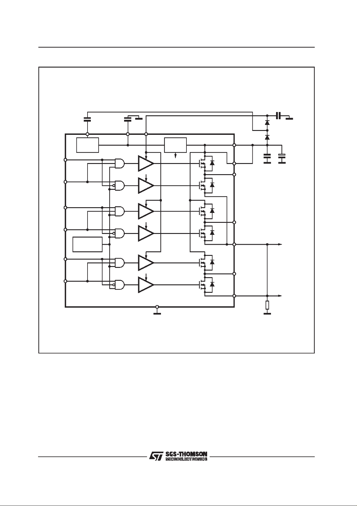
BLOCKDIAGRAM
10nF 1µF
0.22µF
IN1
EN1
IN2
EN2
IN3
EN3
CHARGE
PUMP
THERMAL
PROTECTION
VREFVCP
VBOOT 1N4148
V
=
REF
10V
TH1
TL1
TH2
TL2
TH3
TL3
Vs
7
to 52V
OUT1
OUT2
SENSE1
OUT3
SENSE2
0.1
µF
100µF
2/10
GND
D95IN309A
R
SENSE
THERMALDATA
Symbol Parameter DIP16+2+2 PowerSO20 Unit
R
th j-pin
R
thj-amb1
R
thj-amb2
th j-case
R
Thermal Resistance, Junction toPin
Thermal Resistance, Junction toAmbient
(see Thermal Characteristics)
Thermal Resistance, Junction to Ambient (see Thermal
Characteristics)
Thermal Resistance Junction-case
12 –
40 –
50 –
– 1.5 °C/W
L6234
C/W
°
C/W
°
C/W
°
THERMALCHARACTERISTICS
R
th j-pins
DIP16+2+2
. The thermal resistance is referred to
the thermal path from the dissipating region on
the top surface of the silicon chip, to the points
along the four central pins of the package, at a
distanceof 1.5 mm away from the stand-offs.
R
th j-amb1
If a dissipating surface, thick at least 35 µm, and
with a surface similar or bigger than the one
shown, is created making use of the printed circuit.
Such heatsinking surface is considered on the
bottomside of an horizontalPCB (worstcase).
R
th j-amb2
If the power dissipating pins (the four central
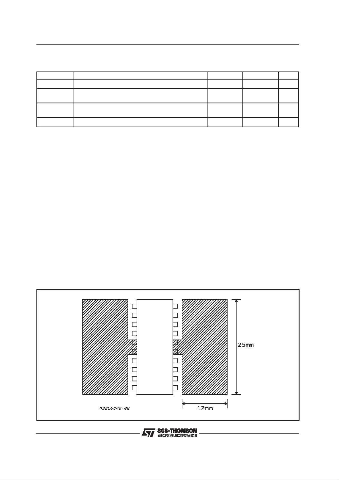
Figure1: Printed Heatsink
ones), as well as the others, have a minimum
thermal connection with the external world (very
thin stripsonly) so that the dissipation takes place
throughstill air and throughthe PCB itself.
It is the same situation of point above,without any
heatsinking surface created on purpose on the
board.
Addition al data on th e PowerDip and th e
PowerSO20 package can be foun d i n:
ApplicationNote AN467:
Thermal Characteristicsof the PowerDip
20,24Packages Solderedon 1,2,3 oz.
Copper PCB
ApplicationNote AN668:
A New High Power IC Surface Mount Package:
PowerSO20 Power IC Packaging from Insertion
to SurfaceMounting.
3/10

L6234
ABSOLUTE MAXIMUM RATINGS
Symbol Parameter Value Unit
V
V
IN,VEN
I
peak
V
SENSE
V
V
OD
f
C
V
REF
P
tot
P
tot
T
stg,Tj
Note 1: Pulsewidth limited onlyby junction temperatureand the transient thermal impedance
(*) Mountedon board with minimized copper area
RECOMMENDEDOPERATINGCONDITIONS
Symbol Parameter Value Unit
V
V
OD
I
out
V
SENSE
T
PIN FUNCTIONS
Powerdip PowerSO20 Name Function
20
10
19
18
4,7 9, 12 V
14 19 SENSE2 A resistance Rsense connected to this pin provides feedback for motor
17 2 SENSE1 A resistance Rsense connected to this pin provides feedback for motor
11 16 V
12 17 V
13 18 V
5,6
15,16
Power SupplyVoltage 52 V
S
Input EnableVoltage – 0.3 to 7 V
Pulsed Output Current (note 1) 5 A
Sensing Voltage (DC Voltage) -1 to 4 V
Bootstrap Peak Voltage 62 V
b
Differential Output Voltage (between any ofthe 3 OUT pins) 60 V
Commutation Frequency 50 KHz
Reference Voltage 12 V
Total Power Dissipation L6234PD T
Total Power Dissipation L6234 T
=70°C 2.3 W
amb
=70°C 1.6 (*) W
amb
Storage and Junction Temperature Range -40 to 150
Supply Voltage 7 to 42 V
S
Peak to Peak Differential Voltage (between any of the 3 OUT
52 V
pins)
DC Output CurrentPower SO20 (T
DC Output CurrentPower DIP (T
=25°C) 4 A
amb
=25°C)with infinite heatsink 2.8 A
amb
Sensing Voltage (pulsed tw < 300nsec) -4 to 4 V
Sensing Voltage (DC) -1 to1 V
Junction Temperature Range -40 to 125
j
1
6
5
15
2
7
4
9
3
14
8
3
8
13
OUT 1
OUT 2
OUT 3
IN 1
IN 2
IN 3
EN 1
EN 2
EN 3
Output of the channels 1/2/3.
Logic input of channels 1/2/3. A logic HIGH level (when the corresponding
EN pin is HIGH) switches ON the upper DMOS Power Transistor, while a
logic LOW switchesON the corresponding low side DMOS Power.
Enable of the channels 1/2/3. A logic LOW level onthis pin switches off both
power DMOS of therelated channel.
Power SupplyVoltage.
s
current control for the bridge 3.
current control for the bridges 1 and 2.
Internal Voltage Reference. A capacitor connected from this pin toGND
ref
increases thestability of the Power DMOS drive circuit.
Bootstrap Oscillator.Oscillator output for the external charge pump.
cp
Overvoltage input to drive the upperDMOS
used to dissipate the heat forward the PCB.
1,10
11,20
BOOT
GND Common Ground Terminal. In Powerdip and SO packages these pins are
C
°
C
°
4/10

ELECTRICALCHARACTERISTICS (Vs= 42V; Tj=25°Cunless otherwisespecified)
Symbol Parameter Test Condition Min. Typ. Max. Unit
V
S
V
ref
I
S
T
S
T
D
Supply Voltage 7 52 V
Reference Voltage 10 V
Quiescent Supply Current 6.5 mA
Thermal Shutdown 150 °C
Dead Time Protection 300 ns
OUTPUT DMOSTRANSISTOR
Symbol Parameter Test Condition Min. Typ. Max. Unit
I
DSS
R
DS (ON)
Leakage Current 1mA
ON Resistance 0.3
SOURCEDRAIN DIODE
Symbol Parameter Test Condition Min. Typ. Max. Unit
V
SD
T
RR
T
pr
Forward ON Voltage ISD= 4A; EN = LOW
Reverse Recovery Time IF=4A
Forward Recovery Time
1.2 V
900 ns
200 ns
L6234
Ω
LOGICLEVELS
Symbol Parameter Test Condition Min. Typ. Max. Unit
V
INL,VENL
V
INH,VENH Input HIGH Voltage
I
INL,IENL
I
INH,IENH
Input LOW Voltage
Input LOW Current VIN,VEN=L
Input HIGH Current VIN,VEN=H
CIRCUITDESCRIPTION
L6234 is a triple half bridge designed to drive
brushlessDC motors.
Each half bridge has 2 power DMOS transistors
with R
ON = 0.3Ω. The 3 half bridges can be
ds
controlled independentlyby meansof the 3 inputs
EN3. An external connection to the 3 common
low side DMOS sources is provided to connect a
sensing resistorfor constant current choppingapplication.
The driving stage and the logic stage are designed towork from 7V to 52V.
-0.3 0.8 V
27V
-10
30
IN1, IN2, IN3 and the 3 inputs EN1, EN2, and
A
µ
A
µ
5/10

L6234
Figure1. QuiescentCurrent vs.Supply Volt-
age.
Iq [m A]
10
9
8
7
6
5
4
3
2
1
0
0 8 16 24 32 40 48
Vs [V]
Tj = -40°C
Tj = 25°C
Tj = 100°C
Tj = 130°C
Figure3. TypicalRDS (ON) vs. SupplyVoltage.
RDS (ON)
[Ω]
0.7
0.6
0.5
0.4
0.3
0.2
0.1
0
0 8 16 2 4 32 40 48
Io u t = 4 A
Tj =130°C
Tj =25°C
Tj=-40°C
Vs [V]
Figure2. Normalized Quiescent Current vs.
switching frequency.
Iq/(Iq@500Hz)
1.75
Tj = 25°C
1.5
1.25
1
0.75
0 102030405060
fsw [kHz]
Tj = 130°C
Tj = -40°C
Figure4. Source Drain Forward ON voltage
vs. JunctionTemperature.
VSD [V]
2
1.75
1.5
1.25
1
0.75
0.5
0.25
0
-50-25 0 255075100125150
Iout=4A
Tj [°C]
Figure5. Typical Diode Forward ON charac-
teristics
ISD [A]
5
Tj = 25°C
4
DMO S (ON) DMO S (OFF)
3
2
1
0
00.5 11.5 2
6/10
VSD [V]
Figure6. ReferenceVoltagevs. SupplyVoltage.
Vre f [V]
12
10
8
6
4
2
0
Tj = 25°C
0 1020304050
Vs [V]

L6234
Figure7. Reference Voltagevs. Junction Tem-
perature.
Vref [V]
11
10
9
8
7
6
5
4
3
2
1
0
-50 -25 0 2 5 50 75 100 125 150
Tj [°C]
Vs = 52V
Vs = 24V
Vs = 10V
Vs = 7V
Figure9. PowerSO-20Thermal Resistance
(Mounted on Aluminiumsubstrate)
Figure8. PowerSO-20Transient Thermal Re-
sistance
Figure10. PowerSO-20ThermalResistance
(Mounted on FR4monolayersubstr at e)
Figure11. PowerSO-20:with externalheatsink
Figure12. Thermal Impedance of PowerSO-20
and standard SO20
7/10

L6234
PowerSO-20PACKAGE MECHANICALDATA
DIM.
MIN. TYP. MAX. MIN. TYP. MAX.
mm inch
A 3.6 0.142
a1 0.1 0.3 0.004 0.012
a2 3.3 0.130
a3 0 0.1 0.000 0.004
b 0.4 0.53 0.016 0.021
c 0.23 0.32 0.009 0.013
D (1) 15.8 16 0.622 0.630
D1 9.4 9.8 0.370 0.386
E 13.9 14.5 0.547 0.570
e 1.27 0.050
e3 11.43 0.450
E1 (1) 10.9 11.1 0.429 0.437
E2 2.9 0.114
E3 5.8 6.2 0.228 0.244
G 0 0.1 0.000 0.004
H 15.5 15.9 0.610 0.626
h 1.1 0.043
L 0.8 1.1 0.031 0.043
N10°(max.)
S8°(max)
T 10 0.394
(1) ”Dand F” do not includemold flashor protrusions.
- Mold flashor protrusionsshall not exceed0.15 mm (0.006”).
- Criticaldimensions: ”E”,”G” and”a3”
E2
hx45°
NN
a2
A
b
DETAILA
110
e3
D
T
e
1120
E1
R
DETAILB
PSO20MEC
lead
a3
Gage Plane
E
DETAILB
0.35
S
a1
L
c
DETAILA
slug
-C-
SEATINGPLANE
GC
(COPLANARITY)
8/10

POWERDIP 20PACKAGE MECHANICAL DATA
L6234
DIM.
MIN. TYP. MAX. MIN. TYP. MAX.
a1 0.51 0.020
B 0.85 1.40 0.033 0.055
b 0.50 0.020
b1 0.38 0.50 0.015 0.020
D 24.80 0.976
E 8.80 0.346
e 2.54 0.100
e3 22.86 0.900
F 7.10 0.280
I 5.10 0.201
L 3.30 0.130
Z 1.27 0.050
mm inch
9/10

L6234
Informationfurnished isbelievedto beaccurateandreliable.However,SGS-THOMSONMicroelectronicsassumesnoresponsibilityforthe
consequencesofuseofsuchinformationnorforanyinfringementofpatentsorotherrightsofthirdpartieswhichmayresultfromitsuse.No
licenseisgrantedbyimplicationorotherwiseunderanypatentorpatentrightsofSGS-THOMSONMicroelectronics.Specificationmentioned
inthispublicationaresubjecttochangewithoutnotice.Thispublicationsupersedesand replacesallinformationpreviouslysupplied.SGSTHOMSONMicroelectronicsproductsarenotauthorizedforuseascriticalcomponentsinlif esupportdevicesorsystemswithoutexpress
writtenapprovalofSGS-THOMSONMicroelectronics.
1998 SGS-THOMSON Microelectronics – Printed in Italy – AllRights Reserved
SGS-THOMSON Microelectronics GROUP OF COMPANIES
Australia - Brazil - Canada - China - France- Germany - Italy- Japan - Korea - Malaysia - Malta - Morocco - The Netherlands -
Singapore - Spain - Sweden - Switzerland- Taiwan - Thailand - United Kingdom - U.S.A.
10/10
 Loading...