

1.5A MAXIMUMPEAKCURRENT
CONTROLLEDSLEWRATE
CENTRAL CHARGE PUMP
PWMAND LINEARMODES
CUTOFFTIME USER CONFIGURABLE
FAST,FREE-WHEELINGDIODESON CHIP
OVER-TEMPERATUREPROTECTION
BRAKEFUNCTIONINPUT
SPINDLE DRIVER
PLCC21+7
ORDERING NUMBER:
L6232E
L6232E
DESCRIPTION
The L6232E is a triple half bridge driver intended
for use in brushless DC motor applications. This
part can be used to form the power stage of a
three-phase, brushless DC motor control loop,
and is especiallyuseful for disk drive applications.
Power drivers are Integrated DMOS transistors
and featurefast recirculatingdiodes as an integral
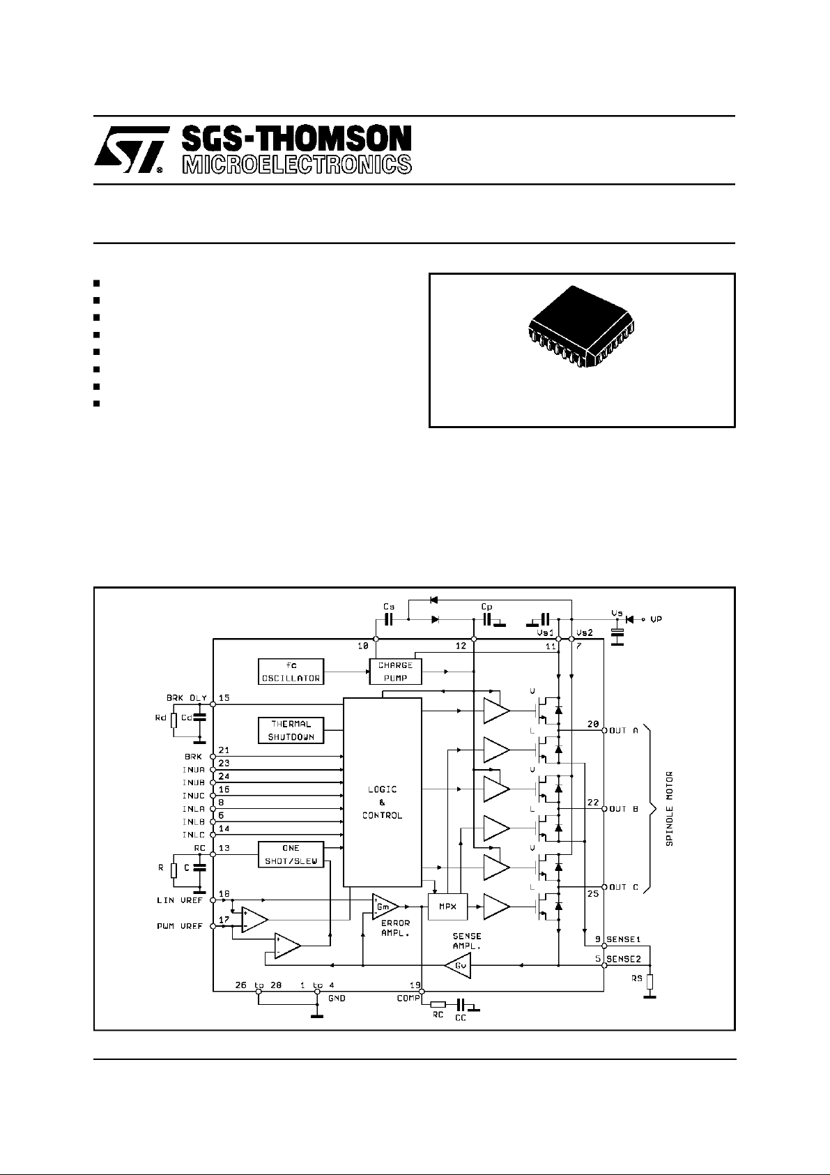
BLOCK DIAGRAM
part of their structure. The logic inputs are TTLlevel compatible, with internal pull-up, allowing interfacing to open collector outputs. All necessary
circuitry to perform PWM and linear motor speed
control is included. A central charge pump is utilized to drive the upper DMOS transistors, and
also to power the braking function.The L6232E is
packagedin PLCC28.
October 1996
This is advanced information on a new product now in development or undergoing evaluation. Details are subjectto changewithout notice.
1/10
L6232E
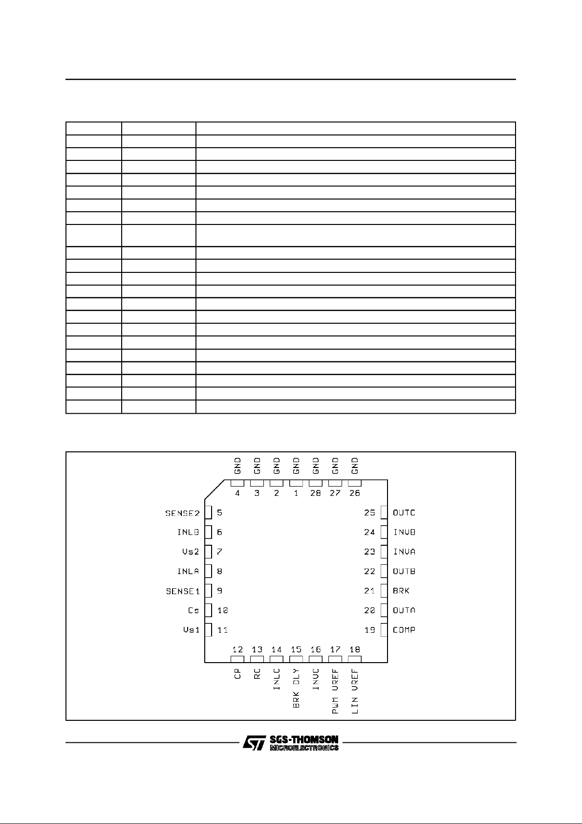
PIN DESCRIPTION
Pin Name Function
1 to 4 GND Common Ground. Also provides heat-sink to PCB.
5, 9 SENSE Output for current sense resistors.
6 INLB Logic Input to turn on the lower driver(Active High).
7, 11 V
S
8 INLA Logic input to turn on the lowey driver (Active High).
10 C
12 C
S
P
13 RC Cutoff Time RC Network in PWM mode. The Resistor value is also used to define
14 INLC Logic input to turn on the lower driver (Active High).
15 BRK DLY External RC network for the brake delay.
16 INUC Logic Input to turn on the upper driver (Active Low).
17 PWM Vref Input for Reference Controlin PWM mode
18 LIN Vref Input for Reference Controlvoltage inLIN mode
19 COMP External compensation for error amplifier
20 OUTA DMOS Half-bridgeA Out.
21 BRK Active LOW logic input thattriggers the delayed brake.
22 OUTB DMOS Half-bridgeB Out.
23 INUA Logic Input to turn on the upper drivers (Active Low).
24 INUB Logic Input to turn on the upper drivers (Active Low).
25 OUTC DMOS Half-bridgeC Out.
26 to 28 GND Common Ground. Also provides heat-sink to PCB.
Supply Voltage.
External Charge Pump Capacitor.
External Main Charge Pump capacitor.
the slew-rate in linearmode (LIN).
PIN CONNECTION
(Topview)
2/10
ABSOLUTE MAXIMUM RATINGS
Symbol Parameter Value Unit
V
DS sus
V
V
Opeak
V
V
V
P
T
stg,Tj
Cp
V
REF
I
p
I
O
tot
Peak Output Sustaining Voltage 15 V
Supply Voltage 15 V
S
Output Peak Voltage (tpK =5µsec; 10% d.c.) 18 V
Charge Pump Input Voltage 30 V
Logic Input Voltage -0.3 to 7 V
i
PWM VREF--LIN VREF Input Voltage -0.3 to 7 V
Sense Input Voltage -1 to 7 V
is
Sink-Source Peak Output Current (*) 3.5 A
Sink-Source DC Output Current 1.8 A
Total Power Dissipation (T
=70°C) 1.5 W
amb
Storage and Junction Temperature -40 to 150
THERMAL DATA
Symbol Description Value Unit
R
th j-pin
R
th j-amb
Notes
(*) Pulse width (limited only by junction temperature and by the transient thermal resistance.
(**) Mounted on board with 16cm
Thermal Resistance Junction-pins
Thermal Resistance Junction-ambient (**)
2
35µm thickness copperarea on board heatsink.
Max.
Max.
14
52
L6232E
C
°
°C/W
C/W
°
ELECTRICALCHARACTERISTICS
=25°C, unless otherwise specified)
T
j
(See the block diagram, V
=12V,R = 100KΩ; C = 180pF;
S
Symbol Parameter Test Condition Min. Typ. Max. Unit
V
S
I
S
Supply Voltage 10.5 12 13.5 V
Quiescent Supply Current BRK = L; INUA = INUB = INUC
0.3 0.5 mA
= L; INLA = INLB = INLC = H;
Table 1
BRK = H; INUA = INUB = INUC
46mA
= H; INLA = INLB = INLC = L;
Table 1
I
OL
R
DSon
R
DSon
V
F
Output Leakage Current VO=VS= 13.5V 1 mA
Sink Out ON Resistance Tj=25°C (see Fig.4) 0.42 0.47 Ω
= 125°C 0.7
T
j
Source Out ON Resistance Tj=25°C (see Fig.4) 0.42 0.47
= 125°C 0.7 Ω
T
j
Body Diode Forward Drop (sink
IDS= 1A (seeFig. 6) 1 1.5 V
and source)
t
d(BRK)
T
BRK
I
B(LIN)
I
B(PWM)
LIN V
PWM V
G
v
Brake Delay Time See Fig. 1, 3; note1 210 ms
Braking Time 10 s
LIN Vref Input Bias Current LIN V
PWM Vref Input Bias Current PWM V
Reference Voltage Input Note 2; RS= 0.5Ω
ref
I
ref
I
Sense Amplifier Voltage Gain PWM V
LIN V
R
= 0.4 to 5.5V 400 950 nA
ref
= 0.4 to 5.5V 400 950 nA
ref
(PWM) = 1A
motor
(LIN) = 200mA
motor
= 2.5V,
ref
= 0.4V,
ref
= 0.5Ω; Note 2
S
3.7 4 4.3 V/V
2V
0.4 V
Ω
Ω
3/10

L6232E
ELECTRICALCHARACTERISTICS
(continued)
Symbol Parameter Test Condition Min. Typ. Max. Unit
G
m
LIN Error Amplifier
0.8 mA/V
Transconductance
Zout Error Amplifier Output
2MΩ
Impedance
V
INH
V
INL
I
INH(leak)
I
INL
t
donU
t
donL
t
doffU
t
doffL
dV/dt Source DMOS Slew-Rate
Logic Input Voltage BRK; INUA;
INUB; INUC; INLA; INLB; INLC
Logic Input Current BRK;INUA;
INUB; INUC; INLA; INLB; INLC
Vi= 2.7V -1 mA
Vi= 0.4V -0.1 mA
2V
0.8 V
Upper/Lower Turn-on Delay Table 1 see Fig. 3 0.7 µs
0.15 µs
Upper/Lower Turn-off Delay 15 µs
0.5
see Fig. 3 10 V/µs
(PWM)
dV/dt Source DMOS Slew-Rate (LIN) see Fig. 3 1 V/µs
dV/dt Sink DMOS Output Turn-off
Note 3; R = 100KΩ 0.15 V/µs
Slew-Rate
F
C
T
off
Internal Clock Frequency 380 KHz
PWM Cutoff Time R=100KΩ; C=180pF, Note 4;
40 µs
see Fig. 2
T
sd
T
sdr
Notes:
1) The Head Park time must be shorter than the Brake Delay time t
2) Both in PWM and in LIN mode the Ref. Voltage must agree to V
3) The resistance of theRC network defines the dv/dt value.
= 1.8RC + 6 ⋅ 10
4) t
off
Shutdown Temperature 160 °C
Recovery Temperature 120
d(BRK)=RdCd
ref=GVRSImotor
-6
s
µ
C
°
Table 1
INPUT STATE OUTPUT STATE
INUA INUB INUC INLA INLB INLC A B C
LLLHHH* * *
LLLLLLHHH
HHHLLL * * *
HHHHHHLLL
H = The Upper DMOS is ON
L = The Lower DMOS is ON
* = Tristatecondition
4/10

L6232E
Figure 1: Brake Delay and Brakingtiming of the L6232E.At the timet1 a VPPowerdownthreshold
detectordrives low the BRK input; at time t2 the Charge Pump voltage becomesinadequate
to maintain ON the lower DMOS.
FUNCTIONAL DESCRIPTION
(Refer to the
Block Diagram)
The commutation sequence is provided by the
user via six inputs. INUA,INUB,INUC turn on the
three upper DMOS drivers when held at logic
LOW, and inputs INLA,INLB,INLC turn on the
three lower DMOS drivers when held at logic
HIGH.
The BRK and BRK DLY inputs offer flexibility to
the system designer in the implementation of the
braking function. The BRK logic input, when
pulled low will turn-off all upper and lower Dmos
drivers. The low transition at BRK will produce a
delayed negativetransition at the BRKDLY input,
configurable by connection of a capacitor Cd and
a resistor Rd from the BRK DLY pin to ground.
The negative transition at BRK DLY will initiate
the braking of the motor by turning on all lower
Dmos, while keeping all upper DMOS turned-off.
This feature provides a time interval where the
motor BEMF can be used to power the head
parking function before the braking procedure is
iniziated. External detection of the supply(VP)
drop-off is necessary to provide the appropriate
logic signal to the BRK input. (see Fig. 1)
The brake function utilizes the energy stored in
the central charge pump capacitor(Cp) to turn-on
or turn-off the DMOS drivers. This allows for
completion of the braking procedure after the VP
supply has powered down.
The L6232E is capable of driving the motor in
either pulse width modulation (PWM) or linear
(LIN) mode. The driving mode is determined by
the smaller of two analog voltages inputs, LIN
Vref and PWM Vref. The motor current is controlled by LIN Vref and PWM Vref and the current
sense resistor Rs connected to the SENSE output. The SENSE output provides for connectionof
a resistor in series with the source of all lower
DMOS drivers. The voltage at this pin provides
the error signal wich is utilized internally to regulate the motor current Im. The current in both
PWM and linear mode is determined by the expression:
V
ref
=
I
m
G
⋅ R
V
S
in wich Gv is the voltage gain of the sense amplifier. In linear mode, the current is regulated by a
linear control loop wich drives the lower DMOS.
Compensation of the linear control loop is
achieved by connection of a series network
(Rc,Cc) from the transconductance amplifier output (Gm) and ground. Control is passed to each
lower DMOS in succession during the commutation sequence(MPX).
The rate at which the upper and lower drivers
turns-off during linear mode operation is configurable externally by the value of the resistor R used
at the RC pin. This defines a current which is utilized internally to limit the voltage slew-rate at the
outputs during transitions. The output slew-rate is
internally adjusted for fast slewing during PWM
operation to reduce losses, and a relatively
slower rate during linear mode operation to mini-
5/10

L6232E
mize noise effects(EMI). LIN Vref and PWM Vref
are connected to a comparator whose output is
fed to the logic . The upper and lower DMOS
driver slew-rates are controlled by the internal
logic.
In PWM mode, the upper driver is turned-offwhen
the motor current reaches the intended value. An
internal One-Shot pulse determines the lenght of
time the upper driver stays off before turning on
again. The pulse width, and thus the cutoff time
(toff), is configurableby means of the externalRC
networkconnectedto the RC pin. (see Fig. 2). The
resistor at the RC pin, therefore determines both
the driver output slew-rate during linear mode and
the off-time constantduringPWM. The lowerdriver
is always on during PWM mode of operation; an
on-chip 2µs mask can prevent the beginning of a
new cutofftime becauseof transientcurrent spikes
causedby theupper driversturn-on.
The driving mode is determinedby the smaller of
the two controlling input voltages. In a typical application the motor start-up would occur in PWM
mode to limit power dissipation, with on-speed
control then performedin linear mode.
Thermal protectioncircuitry will shut-off all drivers
when the chip junction temperature exceeds the
threshold temperature. A small amount of hysteresis is included to prevent rapid on/off cycling of
the power stages.
Additionalprotectionis providedagainstdriverinput
combinationswhere the upperand lower drivers of
a half bridge are turnedon simultaneusly, resulting
in a short from supplyto ground.The chip logic will
causeboth the upperand lower driversinvolvedto
turn-off.(seeTable1)
APPLICATIONINFORMATION
A typical application configuration of the L6232E
driving a three-phase brushless DC motor is
shown in Fig.3. The spindle motor is a 4 ohm2mH per phase, star connected. This load requires a suitable compensation of the linear control loop that can be achieved by Rc= 10 Kohm
and Cc= 10nF (R3;C8). Changing the motor characteristics, the RcCc network would be modified
for the best performances of the system. At the
start-up the spindle is driven in PWM mode fixed
toff time.
The off-time is calculatedby the formula:
toff = 0.69R2 C7
See fig.2 for a quick choiceof the needed capacitor, after the resistor has been fixed. The value of
the resistor defines the rate at which the upper
and lower drivers turn-off during linear mode operation to avoid EMI effects. During turn-off, the
slew rate is constant for the sink stage, while it
has a varying slope for the source stage because
of thenon linear change of the gate to source impedance of the DMOS transistor. Practically, the
Figure2: Typicalt
vs. Capacityof C
off
slowest slew rate is obtainedat the sink transistor
switch-off time (see fig. 5), then it increases during the first period of the source transistor switchoff (source,1st)and it becomes the fastest during
the final portion of the turn-off duration (source,
2nd). The PWM to linear mode of operation is
switched by decreasing the LIN Vref level under
the PWM Vref value that could be fixed and calculatedby:
PWMVref = 4 Rs Ip
where Ip is the peak chopping current in the motor windings. Of course, when the required RPM
is reached, it become of no need a strong torque
and the LIN Vref starting from a value higher than
the calculated PWM Vref, decreases to the value
:
LINVref = 4 Rs Im
whereIm, smaller thanIp, is the neededmotorcurrentto keep constantspin. This last referencevoltage is generally a PLL output driven by speed
transducerscoupled to the spindle (like Hall effect
sensors or BEMF processors). To drive the upper
DMOS and during the brake function a voltage
higher than the supply Vs is needed. The charge
pump integrated in the L6232E keeps C3 at the
correct voltage. To guarantee efficient braking of
the motor , C3 must be chosen of adeguatequality
(very high equivalent parallel resistance). C4 can
be a ceramic disk capacitor . The typical application od the L6232E is in HDD systems on which
thereis theneed to park theRead-WriteHeads before the motor braking. This behavior is possible
with the circuit of Fig.3.At PowerSupplyswitch-off
(see Fig. 1), VP falls down and drives down the
BRK input (Active Low). D1 insulates the L6232E
from the power suppyoutput while the power output stage is switched in a high impedance state.
Thespindlemotor actingas a three-phasealternator supplies the Heads voice coil motor driven
through integrateddiodesthat rectifiethe EMF. After a delay longer than the parking time, the lower
outputDMOSare switched-onand the spindlemotor is braked.The brake delaytime is tipically 150
msecand it isdefinedby :
6/10

L6232E
td(BRK)= 1.4 R1 C6
The sensing resistor value is generally lower
than 1ohm, but a wire wounded type must be
avoided. In Fig.3 the 0.33 ohm sensing resistor
is shown as three parallel 1ohm metal film resis-
Figure 3:
TypicalApplicationCircuit
tors. Care must be taken in the PC Board design
particularly about ground loops and ground copper area. ThetypicalThermalResistancejunction
to ambient versus PC Boardcopper area (Fig.7)
is shown in Fig 8. For Transient Thermal Resistancesee Fig. 9.
Figure 4: Typical NormalizedR
JunctionTemperature
DS (on)
vs.
Figure5: OutputVoltageSlewRate Control vs.
Value
1/R
2
7/10

L6232E
Figure 6: Typical Body Diode Forward Drop vs.
Drain to SourceCurrent.
Figure 8:
TypicalR
vs. On-Board Heatsink
th j-amb
Sidel.
Figure7:
Figure9:
OnBoard Dissipation Copper Area Size
TypicalTransient R
in SinglePulse
th
Condition.
8/10

PLCC28 PACKAGEMECHANICALDATA
L6232E
DIM.
MIN. TYP. MAX. MIN. TYP. MAX.
A 12.32 12.57 0.485 0.495
B 11.43 11.58 0.450 0.456
D 4.2 4.57 0.165 0.180
D1 2.29 3.04 0.090 0.120
D2 0.51 0.020
E 9.91 10.92 0.390 0.430
e 1.27 0.050
e3 7.62 0.300
F 0.46 0.018
F1 0.71 0.028
G 0.101 0.004
M 1.24 0.049
mm inch
M1 1.143 0.045
9/10

L6232E
Information furnished is believed to be accurate and reliable. However, SGS-THOMSON Microelectronics assumes no responsibility for the
consequences of use of such information nor for any infringement of patents or other rights of third parties which may result from its use. No
license is granted by implication or otherwise under any patent or patent rights of SGS-THOMSON Microelectronics. Specification mentioned
in this publication are subject to change without notice. This publication supersedes and replaces all information previously supplied.
SGS-THOMSON Microelectronics products are notauthorized foruse as criticalcomponents in lifesupport devices or systems without express
written approval of SGS-THOMSON Microelectronics.
1996 SGS-THOMSON Microelectronics – Printed in Italy – All Rights Reserved
SGS-THOMSON Microelectronics GROUP OF COMPANIES
Australia - Brazil - Canada- China - France - Germany - HongKong - Italy - Japan - Korea - Malaysia - Malta- Morocco - The Netherlands -
Singapore - Spain - Sweden - Switzerland- Taiwan- Thailand - UnitedKingdom - U.S.A.
10/10
 Loading...