

L6223
DMOS PROGRAMMABLE
HIGH SPEED UNIPOLAR STEPPER MOTOR DRIVER
HIGH EFFICIENCY UNIPOLAR STEPPER
MOTORDRIVER
HIGH SPEED UNIPOLAR STEPPER MOTOR
DRIVER
SUPPLYVOLTAGE UP TO 46V
PHASECURRENT UP TO 1A
UP TO 2A/PHASE IN DUAL CONFIGURA-
TION
PARALLEL CMOSµP INTERFACE FOR
FULL/HALFSTEP MOTOR ROTATION
SERIAL INTERFACE FOR 6 BIT PROGRAM-
MING
CLOSE/OPEN LOOP, 8 PWM CURRENT
LEVELS
DUAL PWM FREQUENCYSELECTION
INPUTBIDIRECTIONALLYPROTECTED
THERMALSHUTDOWN
DESCRIPTION
The L6223 is a programmable integrated system
for driving a unipolar stepper motor. It is realized
in Multipower BCD technology. The DMOS output
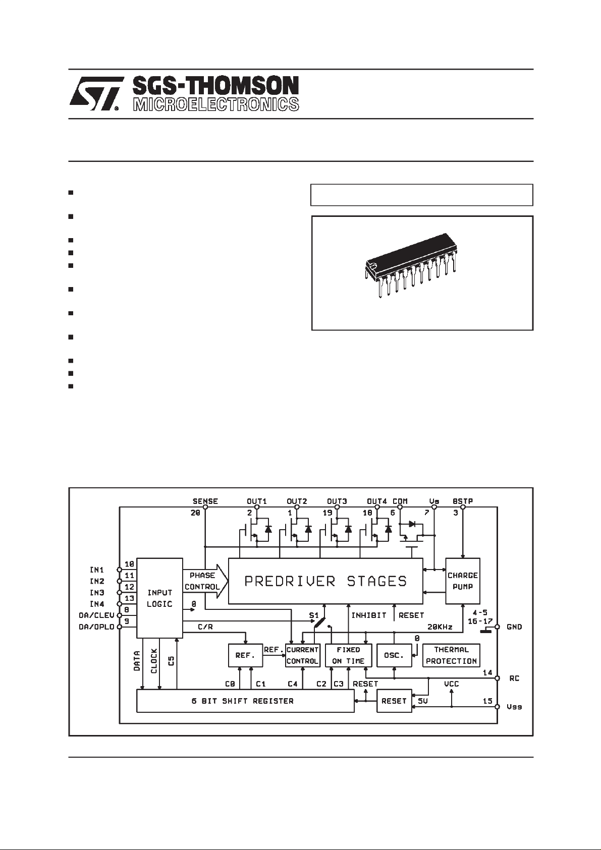
BLOCKDIAGRAM
MULTIPOWER BCD TECHNOLOGY
POWERDIP
16+2+2
ORDERING NUMBER : L6223
stage, realized by a single upper DMOS switch
and four lower DMOS,can deliverup to 1A/phase
with motor supplyvoltages up to 46V.
All inputsare CMOS and microprocessor compatible. An internal 6-bit shift register allows the device to be programmed to select different duty cycles in open loop mode and different chopping
frequencies in closed loop mode. When the current control is in closed loop mode it is also possible to select a reduced current chopping level to
optimize system efficiency. The L6223 is de-
March 1998
1/33
L6223
signed to work with a single sense resistor. During chopping t(OFF) time the current is reduced
by half, improving efficiency.Higher current appli-
The L6223 is mounted in a 20-lead Powerdip
package, (16+2+2). Four ground leads conduct
heat to dedicated heatsinkarea on the PCB.
cations can be achieved by paralleling two L6223.
ABSOLUTEMAXIMUM RATINGS
Symbol Parameter Value Unit
V
SS
V
S
V
I
V
O
V
Opeak
I
pl
I
ph
P
tot
V
sense
T
stg,Tj
( * ) Oscillator running
(**)4cm
2
copper area on PCB, see fig. 34
PIN CONNECTION
Logic supply 7 V
Supply voltage 50 V
Logic input voltage (*) – 0.3V to V
Output voltage 100 V
Output peak voltage (tpk = 5µs,10% d.c.) 125 V
Output sink peak current d.c. 10% t(on) = 10µs3A
Output source peak current d.c. 10%,t(on) = 10µs6A
Total power dissipation: T
=90°C 4.3 W
pins
=70°C (**) 2 W
T
amb
Sensing voltage – 1V to V
Storage and junction temperature – 40 to 150 °C
( topwiew )
SS
SS
THERMAL DATA
R
thj-pins
R
thj-amb
2/33
Thermal Resistance Junction-pins Max 14 °C/W
Thermal Resistance Junction-ambient Max 60
C/W
°

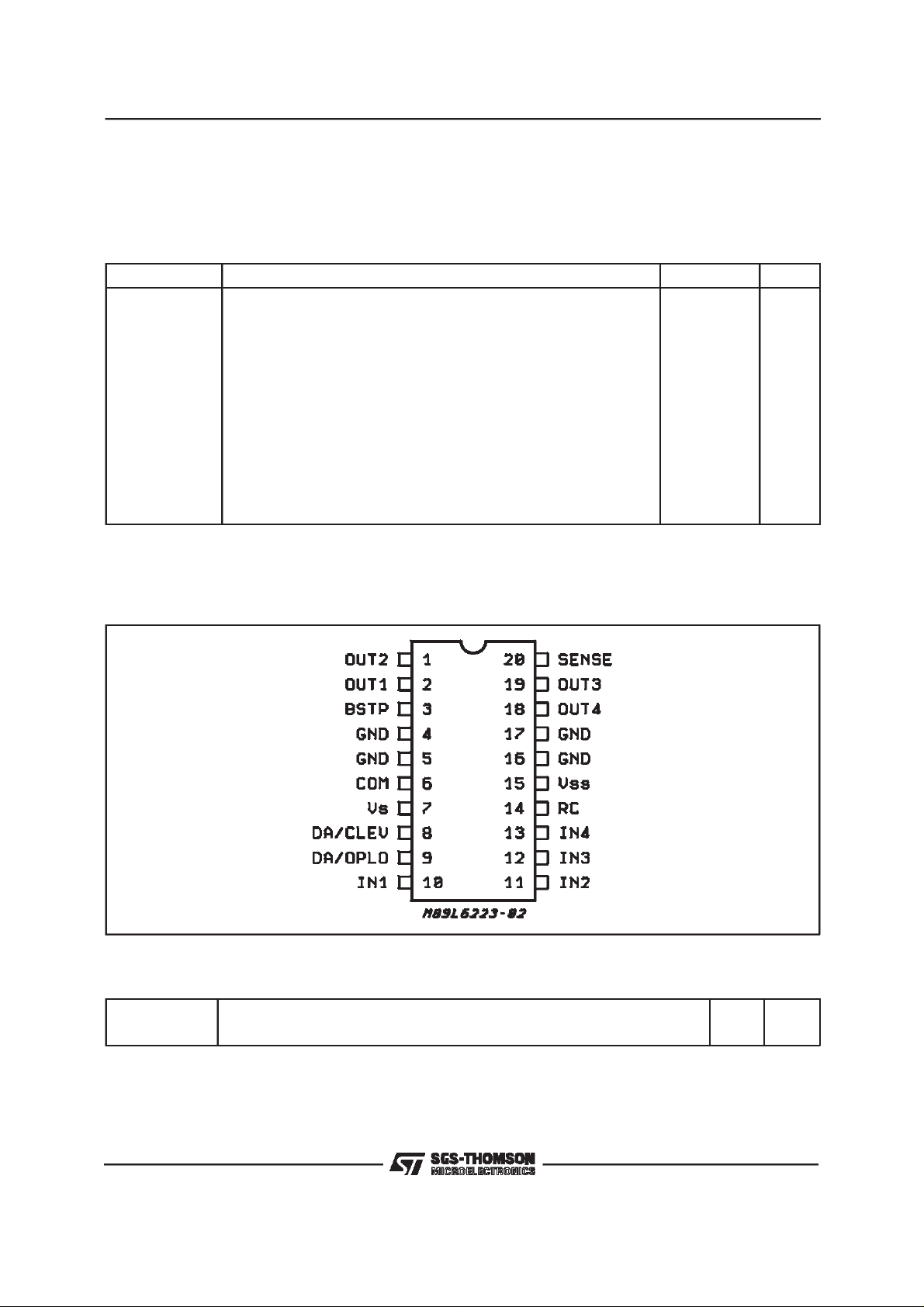
PIN DESCRIPTION
No. Name Function
L6223
1,2
18,19
OUT2,OUT1
OUT4,OUT3
Outputs for motor windings.
3 BSTP A bootstrap capacitor connected between this pin and COM will
generate the internal overvoltage required for driving the gate of the
upper DMOS.
6 COM Output for common wire of motor.
4,5
GND Common ground. Also provides heatsinking to PCB.
16,17
7V
S
Power supply
8 DA/CLEV Digital input.
1) In PROGRAM MODE,operates in XOR withDA/OPLO to load data
into 6-bit shift register.
2) In OPERATING MODE,works with the otherdigital inputs to reduce
the current level (see Table 2 and Table 3).
9 DA/OPLO Digital input.
1) In PROGRAM MODE, operates in XOR with DA/CLEV to load data
into 6-bit shift register.
2) In OPERATING MODE,selects current control method: open loop(H)
or closed loop (L).
10,11
12,13
IN1,IN2
IN3,IN4
Digital inputs. When all inputs are low level,the device is in
PROGRAMMING MODE.
In OPERATING MODE:
1) FULLMODE - IN1 to IN4 drive the motor phases.
A previous programming is requested.
2) SIMPLIFIEDMODE - IN1 and IN2 drive the phases,IN3 is
ENABLE, IN4 works with DA/CLEV to enable the reduce current
level. Previous programming not needed.
14 RC Input for external RC network. Defines the higher of two possible
chopping frequencies. If this pin is set to ground it will reset the IC.
15 V
SS
Logic supply.
20 SENSE Output for sense resistor.
3/33
L6223
ELECTRICAL CHARACTERISTICS (Tj=25°C, VS= 42V,VSS=5V, externalRC network: R =18kΩ,
C = 3.3nF,unlessotherwise specified).
Symbol Parameter Test conditions Min Typ Max Unit
V
S
V
SS
I
S
Power Supply 9 32 46 V
Logic Supply 4.5 5 5.5 V
Power Supply Quiescent
Current
I
SS
Logic Supply Quiescent
Current
I
OL
V
rs
Output Leakage Curr. VO= 100V (Fig. 1) 1 mA
Reset Threshold
Voltage (Pin 14)
T
BOOT
Bootstrap Refresh Pulse C
SINK MOS
R
DS(ON)
ON Resistance (Fig. 2a and Fig. 3) 1.2 Ω
SOURCEMOS
R
DS(ON)
ON Resistance (Fig. 2b and Fig. 3) 0.7 Ω
CURRENT CONTROL SECTION
IN1, IN2, IN3, IN4 = L
24mA
RC = 0V DA/CLEV = L
DA/OPLO = L
IN1, IN2, IN3, IN4 = L
14 20 mA
RC = 0V DA/CLEV = L
DA/OPLO = L
= 10nF 3 5 µs
BOOT
0.9 V
V
ref
f
(OSC)
t
(dis)
R
int
T
W
LOGICLEVELS
V
(IN)L
V
(IN)H
4/33
Internal Reference Volt. DA/CLEV = L; IN4 = H
I
= 100% nominal value
O
0.475 0.5 0.525 V
Oscillator Frequency (Fig. 20) 18 20 22 KHz
RC Network Discharge
Time (t
ON
min)
Internal Discharge Resistor
(Fig. 20) 2.3 3 4.3 µs
1.2 k
Ω
(pin 14)
Sense Filter Time Constant (Fig. 4) 1 1.4 2.3 µs
Input Low Voltage –0.3 0.8 V
Input High Voltage 2.4 V
SS
V
ELECTRICAL CHARACTERISTICS (Continued)
Symbol Parameter Test conditions Min Typ Max Unit
SWITCHINGTIMING
L6223
t2, t4 Fall/Rise Time (IN1, 2, 3, 4) R
t1, t3 Input-Output Delay
t
dPWM
(IN1, 2, 3, 4)
Close Loop PWM
Control Delay
=39Ω(Fig. 5)
(load)
Pure Resistive Load to V
R
=39Ω(Fig. 5)
(load)
Pure Resistive Load to V
(Fig. 4) Note 1 1 µs
S
S
250 ns
700 ns
PROGRAMMING TIMING
t1 Loading Time (Fig. 6) 1.7 µs
t2 Protection Time (Fig. 6) Note 2 0.2 µs
t3 Data Set-up (Fig. 6) 0 ns
t4 Data Hold (Fig. 6) 1.6
t5 Setting Time (Fig. 6) 200 ns
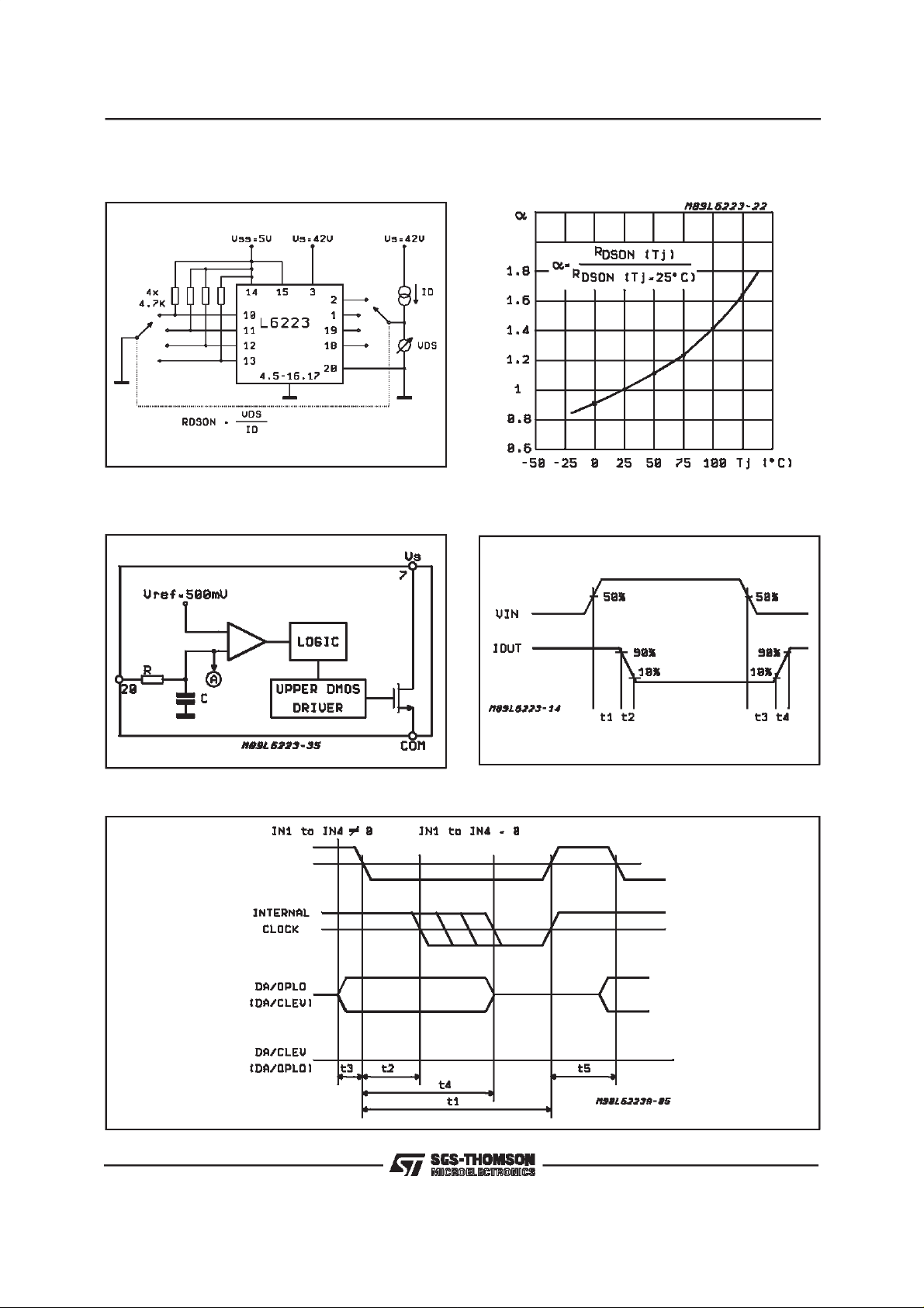
Note 1) Upper DMOS turn ON delay when the signal is applied at the input comparator (point A in Fig. 4).
Note 2) Internal clock pulse isgenerated only if IN1...IN4 stay Low for almost 0.2 µs. This delay avoids undesirable programmings.
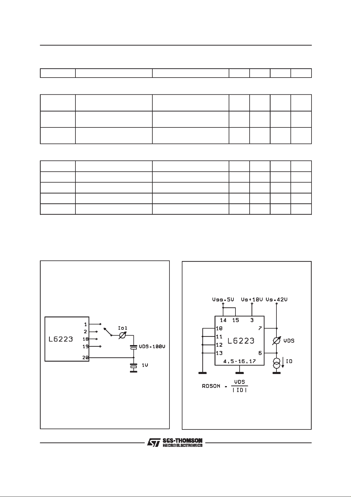
Figure1:
Outputleakage I
Test Circuit
OL
Figure2a:
Source Output DMOS R
DS(ON)
Circuit
µ
Test
s
5/33
L6223
Figure2b:
Figure4:
SinkOutput DMOSR
DS(ON)
Test Circuit
SenseFilterRCTimeConstantandPWM
ClosedLoop control Circuit
Figure3:
Figure5:
Typical normalized R
DS(ON)
vs. Junction
temperature
OutputSink Current Delay vs Input
Control
Figure6:
6/33
ProgrammingTiming Diagram(see Block Diagram)

L6223
BLOCKDIAGRAM DESCRIPTION
InputLogic
Decodes the input signals IN1, IN2, IN3, IN4,
DA/OPLO, and DA/CLEV for programming the
device and driving the motor. The six inputs are
CMOS compatible and can interface directly with
a microprocessor.
PredriverStages
Drive the gates of the five DMOS. They interface
the power section with the logic section. The internal inhibit, when activated, disables the power
section. The reset initializes the shift register and
disables the power section.
6 bit Shift Register
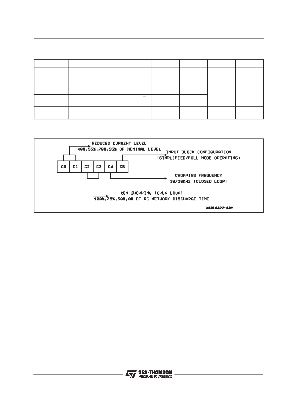
Internal memory which defines the working configuration of the device along with the input signals.
Current Control
When selected with the input DA/OPLO = L
(Closed Loop), it will maintain a constant output
current level by chopping. The value of the reference voltage, which is compared to the sense
voltage, is given by the Ref Block. The chopping
frequencydepends on bit C4.
Ref Block
Defines the current chopping level according to
bits C0 and C1 and the inputsignals.
Fixed on Time
When selected with DA/OPLO = H, it will define
accordingto bits C2 and C3 the chopping duty cycle for the Open Loop mode. The chopping frequencyis fixed.
Oscillator
Provides the clock setting the S/R FLIP-FLOP
that turn ON/OFF the upper DMOS (Fig. 22). The
higher operative chopping frequencyis defined by
the external RC network (typically 20KHz). At the
phase change a syncronous clock pulse is generated
Reset Logic Block
Generates the reset signal for the logic at power
on and disables the outputs. The reset can also
be generated externally by setting the RC pin to
less that 0.9V.
ThermalProtection
Disables the power section in case of over temperaturecondition.
Charge Pump
Along with an external bootstrap capacitor connected between the BSTP and COM pins, this
block generates the internal over voltage required
to drive the upper DMOS on.
PowerOutput
Driven by the Predriver Stages, it supplies the
power for the motor windings.
CIRCUIT OPERATION
The five N DMOS transistors of the output stage
drive the unipolar motor windings, controlling the
current by chopping. In particular, the four Low
side (OUT1, OUT2, OUT3, OUT4) switch the
phase configurations, and the High side DMOS
(COM)is for chopping control.
For this transistor a charge pump circuit provides
its necessarygate drive over voltage.
The microprocessor outputs are interfaced with
the L6223 output stages through the input logic
block. This block also protects the devicefrom microprocessor output errors and failures from the
power section back to the microprocessor outputs. The six digital inputs IN1, IN2, IN3, IN4,
DA/CLEV, DA/OPLO, are decoded for motor control and rotation when in ”Operating mode” and
used for the internal six Bit memory programming
when in ”ProgrammingMode”.
Table 1 shows the condition that selects these
devicestatus. The programmingof the internal six
bit memory setsoperative conditionssuch as:
•PWM CURRENT LEVELS
•CHOPPINGFREQUENCY
•LOGICIN/OUT DECONDING
This memory works like a shift register.Each bit is
introduced serially by decoding the IN1, IN2, IN3,
IN4 low status for the internal clock pulse generation and by the DA/CLEV DA/OPLO, inputs in
exor, as data in.
Figure 7 shows the six bit meaning.
In theoperating mode two different input drive are
possible. In SIMPLIFIEDOPERATING MODE the
IC needs few logic wire for the motor rotation, but
only the full step driving sequence can be performed.
7/33
L6223
Table 1
Device status Bit C5 IN1 IN2 IN3 IN4 DA/CLEV DA/OPLO
Simplified
mode
operating
Full mode
operating
Programming
mode
Figure7:
L
H
XLLLL
Phase A
Driver
Phase A Phase A
Phase B
Driver
driver
InternalSix-Bit Shift Register Bit Functions
Enable
Phase B
driver
Alternative
Current
Reduction
”LOW”
Phase B
driver
Current
Reductio
Active
”HIGH”
serial
data in
Open/Closed
Loop current
control
serial
data in
CIRCUIT OPERATION
(continued)
The FULL OPERATING MODE permits all the
driving possibilities.The 4 low side DMOS transistors are drived directly by the 4 inputs IN1, IN2,
IN3, IN4 which define directly the phases configuration. The chopping of the motor current can be
in open loop or in close loop. When in open loop
(fixed on-time block) the DA/OPLO pin is High
and the motor current is not controlled but it
mostly depends from the bits C2 nd C3. When in
close loop the DA/OPLO is Low and the output
current is controlled at a constant value defined
by the internal reference and by the sensing resistor value. The internal reference depends by
the programming bits C0, C1, and by the input
configurations.During the power on sequencethe
reset circuitry prevents current spikes disabling
the outputsand by resettingthe memory.
Power Section
The basic concept for the current control is explained by examining the winding pair phase A
(MA) in Figure 24. With Q5 = ON, Q2 = OFF the
current rises until R
equals the comparator
SIP
thresholdvalue. The comparatoroutput resets the
8/33
F/F and Q5 switches off. In this condition the current decay path begins as shown in Figure 25.
The current value becomesI
/2, according to the
p
double number of turns interested. In order to reduce the dissipation, Q2 is also driven on. Q5 remains off (PWM off time) up to a new clock pulse
sets again the F/F.The winding current behaviour
is shown in Figure 26.
Since during PWM off time the current value is
half that of the on time and since in a typical application Toff >>Ton, the device dissipation is further reduced.
The five DMOS transistors are connected to the
”predriver stages” block, that drives the DMOS
gates, and interfaces them to the internal input
logic. The ”charge pump” provides correct voltage
for Q5 UPPER DMOS gate drive by using the external bootstrapcapacitor.
ProgrammingMode
The Programming Mode is defined by the inputs
IN1=IN2=IN3=IN4=Low. When in PROGRAMMING MODE the outputs are disabled. The waveform shown in Fig. 8 represents one possible tim-
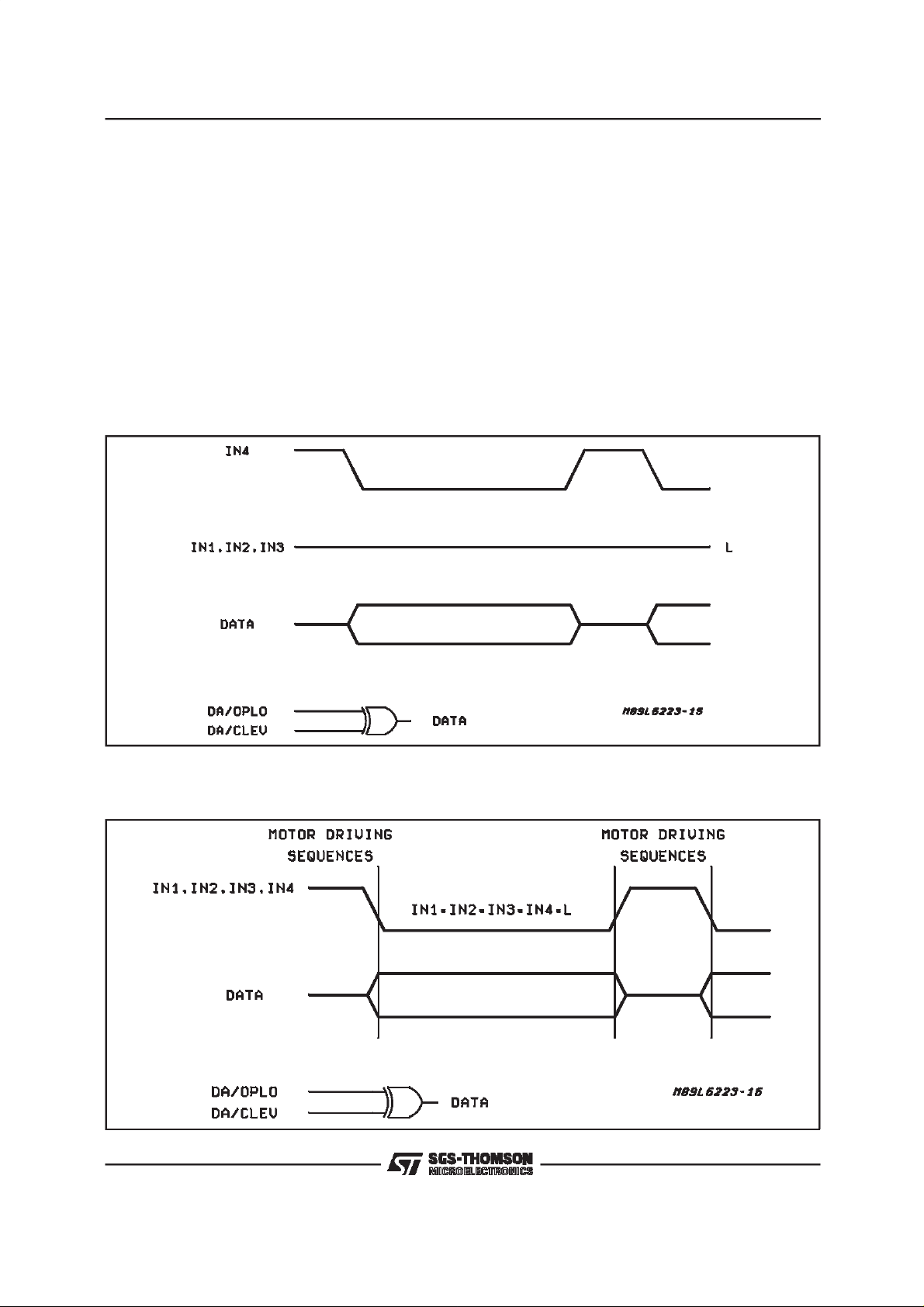
L6223
ing diagram for programming. When the inputs
IN1...IN4 are together Low a clock pulse is generated internally which clocks a data bit into the
shift register. If the time interval during which all
four inputs are Low is less than 0.2µs, no clocks
pulse in generated thus preventing undesirable
programming. To generateanother clock pulse at
least one of the four inputs must first go High and
then Low again. The first bit isloaded into C0 and
after 6 clock pulse it will be in the C5 posistion.
Two programming technique are suggested. The
first (Fig. 8) uses IN4 in such a way that the
Figure 8:
Wavefor mforprogrammi ng:the outputis disabledduringall theprogram mingduration(seeTable 4).
power section is disabled the total programming
time (the carriage of the 6 programmingbits). Fig.
9 shows another technique:the motor driving signals at the inputsIN1...IN4 are interrupted switching IN1...IN4 Low to carry a single bit. This permits the motor to be enabled for the 50% of total
programming time. During the motor rotation it’s
suggested to program the device immediately after the motor phase change: this make neglectable the motor driving discontinuity due to the device programming.
Figure9: Waveform for programming:theoutput is disabled only whenall four inputs are atthe low level.
9/33

L6223
OperatingMode
The bit C5 defines the two available input configurations.
C5 = H: FULL MODE OPERATING
The digital inputshave the following functions:
•
IN1drives OUT1
•
IN2drives OUT2
• IN3drives OUT3
The output DMOS is ON
when the corrisponding input is low
• IN4drives OUT4
• DA/CLEVenablesthe current reduction
(seeTab 2)
•
DA/OPLOselectsthe motor current control
mode(open or closeloop).
Since each input drives one phase of the motor it
is possible to work either in Half Step or in Full
Step mode. DA/OPLO defines the current control
modeas follow:
– DA/OPLO = H open loop
– DA/OPLO = L closedloop
The reduced currentlevel is enabledby the inputs
IN1, IN2, IN3, IN4 or by DA/CLEV (Tab. 2). The
reduced current value dependsfrom the bits C0,
C1 (TAB. 5). The outputs are disabled when the
inputs are in a prohibited state (Tab. 4).
C5 = L, SIMPLIFIED MODEOPERATING
When in SIMPLIFIEDMODE OPERATINGthe in-
puts assumethe following functions:
•IN1 drivesPhase A
•IN2 drivesPhase B
•
IN3 ENABLE input (activeHigh)
•
IN4 enables the reduced current(Tab. 3)
•DA/CLEVenables the reduced current (Tab. 3)
• DA/OPLO selects the motor current control
mode
The SIMPLIFIED MODE OPERATING configura-
tion does not allow the drive of a unipolar motor in
Half step.
The signal DA/OPLO functions as in FULL Mode
Operation. When the current control is implemented in closed loop, the reduced current level
is enabled by the inputs IN4, DA/CLEV (Tab. 3).
The current reduction depends from the bits C0,
C1 (Tab. 5).
Open/ClosedLoopMotor Current Control
The logic input DA/OPLO selects the current control mode as previously seen. When in open loop,
the chopping frequency is that one as defined by
the external RC network. In open loop are available three different t(ON), dependingfrom the bits
C2, C3 (Tab. 6), as a percentage of the RC dischargetime t
(dis)
.
When in closed loop two different chopping frequencies are selectable by means of the bit C4
(Tab. 7). The higher is defined by the external RC
network. The other one is exactely the half. In
closed loop 5 different current levels are available: the nominal current level and four reduced
current levels (Tab. 5). The nominal current level
is set by an internal reference voltage of 0.5V.
The configuration of bits C0, C1 sets the reference voltage to a pecentageof the nominal value.
TRUTH TABLES
(L = Low; H = High; X = don’t
care)
Table 2
IN1 IN2 IN3 IN4 DA/CLEV C/R*
HHXX X H
XXHH X H
HHHH X H
XXXX H H
*) C/R = H,reduced current
Table 3
IN4 DA/CLEV C/R
LXH*
XHH*
H L L**
*) Reducedcurrent **) Nominal current
Table 4
IN1 IN2 IN3 IN4 Output Stage
L L X X DISABLED
X X L L DISABLED
Table 5
C0 C1 Reduced Current Level (*)
L L 40%
L H 50%
H L 70%
H H 85%
*) Nominal level percentage
10/33
 Loading...