

L6 221A L62 21 AD
.
FOURNONINVERTINGINPUTSWITH
ENABLE
.OUTPUT VOLTAGEUPTO50V
.OUTPUT CURRENT UPTO1.8A
.VERYLOW SATURATIONVOLTAGE
.
TTLCOMPATIBLEINPUTS
.INTEGRALFAST RECIRCULATIONDIODES
DESCRIP TION
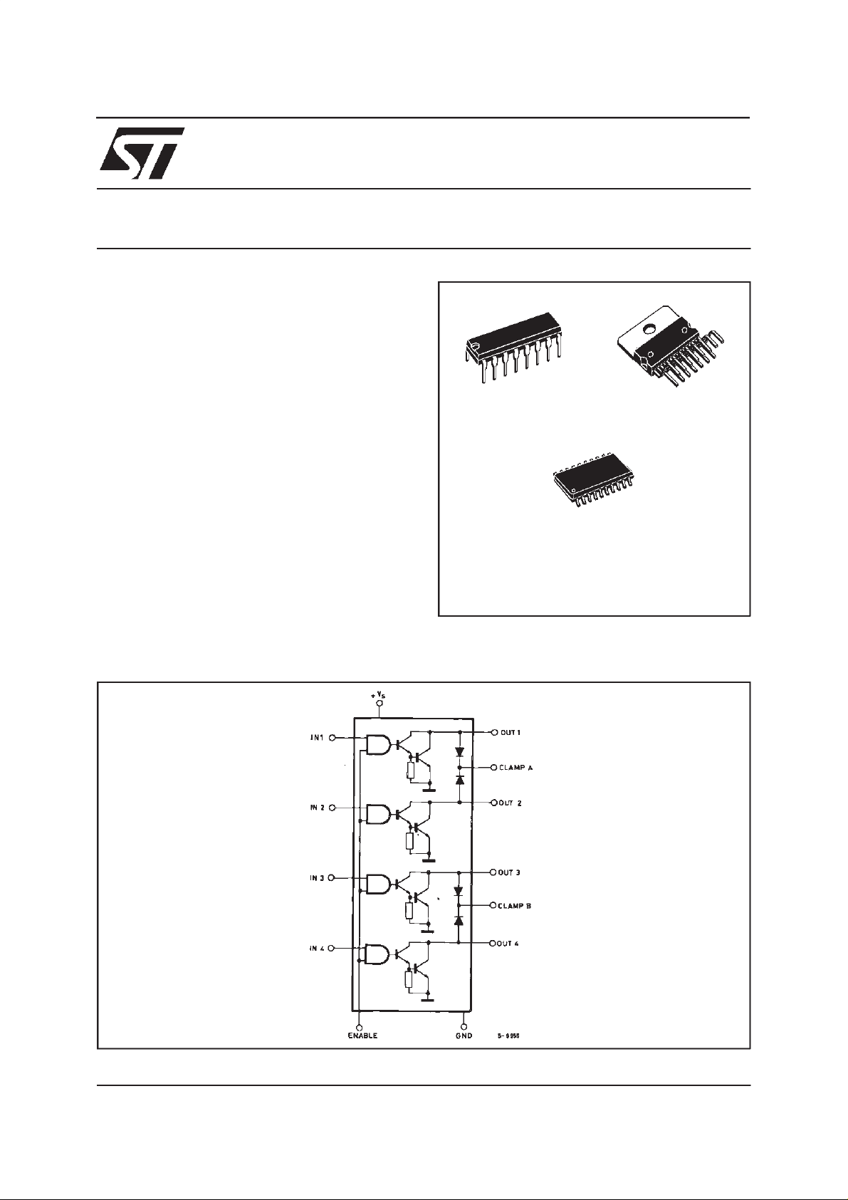
TheL6221monolithicquaddarlington switchis designedforhighcurrent,highvoltageswitchingapplications.Eachof thefourswitchesis controlledby a
logicinput and allfourare controlledby a common
enableinput.AllinputsareTTL-compatiblefordirect
connectiontologic circuits.
Eachswitchconsistsofanopen-collectordarlington
transistorplusafastdiodeforswitchingapplications
withinductivedeviceloads.The emittersof thefour
switchesare commoned.Anynumberofinputsand
outputsof the samedevice maybe paralleled.
L6221N
QUADDARLINGTON SWITCH
Powerdip12 +2 +2
SO16+2+2
ORDERINGNUMBERS:
L6221A(Powerdip)
L6221N (Multiwatt15)
L6221AD (SO16+2+2)
Multiwatt15
BLOCK DIAGRAM
July 1998
1/15

L6221A - L6221AD - L6221N
THERMAL DATA
Symbol Parameter SO20 Powerdip Multiwatt15 Unit
R
th j-pins
R
th j-case
R
th j-amb
Thermal Resistance Junction-pins Max.
Thermal Resistance Junction-case Max.
Thermal Resistance Junction-ambient Max.
17
80
–
–
80
14
–
3
35
C/W
°
C/W
°
C/W
°
PIN CO NNECTI ONS
L6221A (Powerdip)
(top vie ws)
CLAMPB
CLAMPA IN2
L6221N (Multiwatt-15)
L6221AD (SO16+2+2)
OUT4
2
N.C.
OUT3
GND
GND
OUT2
N.C.
OUT1 IN1
3
4
5
6
7
8
9
10
D95IN231
20
19
18
17
16
15
14
13
12
11
IN41
IN3
N.C.
ENABLE
GND
GND
V
N.C.
S
2/15
L6221A - L6221AD - L6221N
ABSOLUTE MAXIMUM RATINGS
Symbol Parameter Value Unit
V
V
V
IN,VEN
I
I
I
T
T
I
sub
P
o
s
C
C
C
op
stg
tot
Output Voltage 50 V
Logic Supply Voltage 7 V
Input Voltage, Enable Voltage V
s
Continuous Collector Current (for each channel) 1.8 A
Collector Peak Current (repetitive, duty cycle = 10 % ton= 5 ms) 2.5 A
Collector Peak Current (non repetitive, t = 10µs)
3.2 A
Operating Temperature Range (junction) – 40 to + 150
Storage Temperature Range – 55 to + 150
Output Substrate Current 350 mA
Total Power Dissipation at T
at T
at T
at T
at T
at T
=90°C (powerdip)
pins
=90°C (multiwatt)
case
=90°C (SO20)
case
=70°C (powerdip)
amb
=70°C (multiwatt)
amb
=70°C (SO20)
amb
4.3
20
3.5
1
2.3
1
°C
°
W
W
W
W
W
W
C
TRUTH TABLE
Enable Input Power Out
H
H
L
Foreach input: H = Highlevel
L = Low level
H
L
X
PIN FUNCTIONS (see block diagram)
Name Function
IN 1 Input to Driver 1
IN 2 Input to Driver 2
OUT 1 Output of Driver 1
OUT 2 Output of Driver 2
CLAMP A Diode Clamp to Driver 1 and Driver 2
IN 3 Input to Driver 3
IN 4 Input to Driver 4
OUT 3 Output of Driver 3
OUT 4 Output of Driver 4
CLAMP B Diode Clamp to Driver 3 and Driver 4
ENABLE Enable Input to All Drivers
V
S
GND Common Ground
Logic Supply Voltage
ON
OFF
OFF
3/15
L6221A - L6221AD - L6221N
ELECTRICAL CHARACTERISTICS
Refer to the test circuit to Fig. 1 to Fig. 9 (V
= 5V, T
S
Symbol Parameter Test Conditions Min . Typ . Max . Unit
V
S
I
s
V
CE(sus)
I
CEX
V
CE(sat)
L, VENL Input Low Voltage 0.8 V
V
IN
L, IENL Input Low Current VIN=VINL, VEN=VENL – 100
I
IN
L, VENH Input High Voltage 2.0 V
V
IN
H,IENH Input High Current VIN=VINH, VEN=VENH
I
IN
I
R
V
F
t
d (on)
t
d (off)
I
∆
Logic Supply Voltage 4.5 5.5 V
Logic Supply Current All Outputs ON, IC= 0.7A
All Outputs OFF
Output Sustaining Voltage VIN=VINL, VEN=VENH
= 100 mA
I
C
Output Leakage Current VCE= 50V
V
IN=VIN
Collector Emitter Saturation Voltage
(one input on ; all others inputs off.)
Vs= 4.5V
V
IN=VIN
= 0.6A
I
C
=1A
I
C
= 1.8A
I
C
Clamp Diode Leakage Current VR=50V,VEN=VENH
V
IN=VIN
Clamp Diode Forward Voltage IF=1A
= 1.8A
I
F
Turn on Delay Time
Turn off DelayTime
Logic Supply Current Variation VIN= 5V, VEN=5V
s
= 5V, RL=10
V
p
= 5V, RL=10Ω
V
p
= – 300mA for Each Channel
I
out
=25oC unless otherwise specified)
amb
46 V
L, VEN=VENH
H, VEN=VENH
L
Ω 2 µ
2020mA
1mA
1
1.2
1.6
10
±
100 µ
1.6
2.0VV
5
120 m A
mA
V
µ
µ
µs
A
A
A
s
4/15
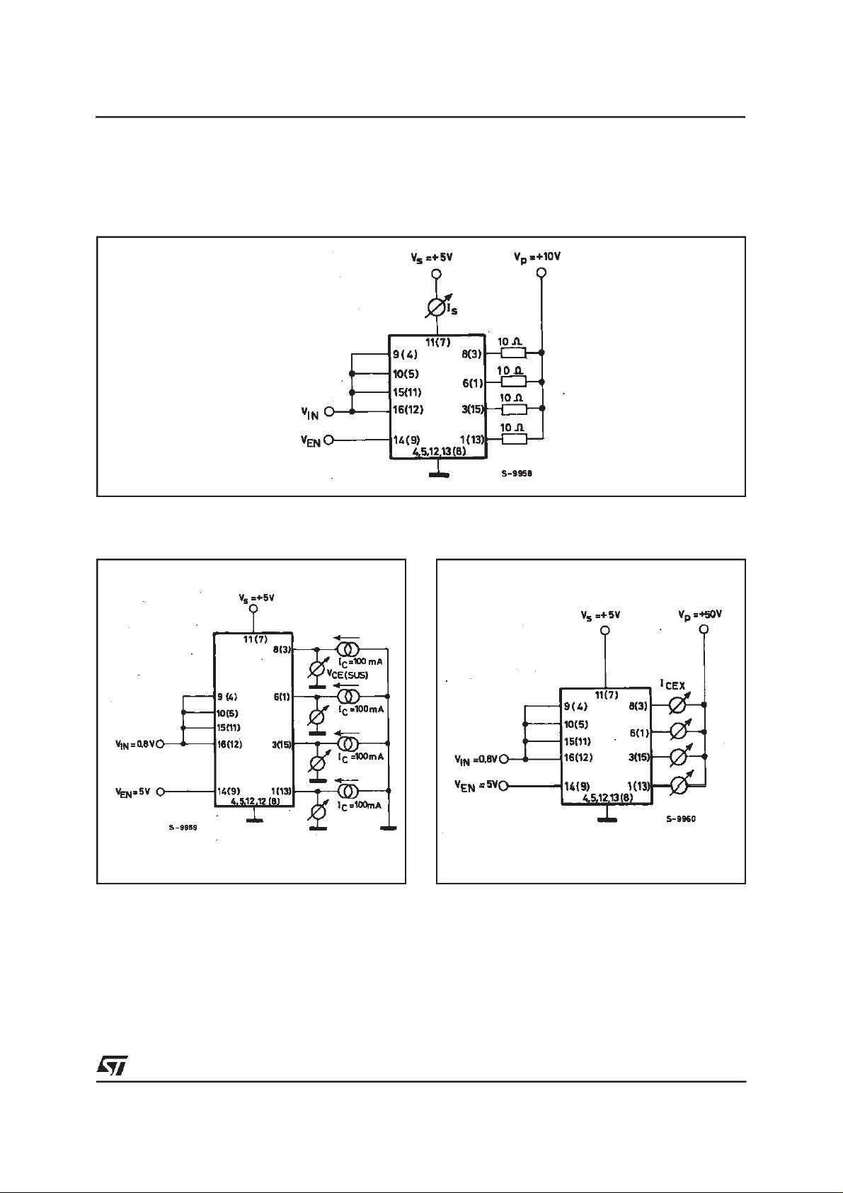
TEST CIR CUITS
(X)= Referredto Multiwattpackage
X = Referredto Powerdippackage
Figure 1 : Logic supply current.
SetVIN= 4.5V,VEN= 0.8V,or VIN= 0.8V,VEN=4.5V, for IS(alloutputs off)
S
= 2V, VEN= 2V, for IS(alloutputson)
etVIN
L6221A - L6221AD - L6221N
Figure 2 : Output SustainingVoltage. Figur e 3 : Output Leakage Current.
5/15
 Loading...