

.
FOURNONINVERTINGINPUTSWITH
ENABLE
.
OUTPUTVOLTAGEUPTO 60 V
.OUTPUTCURRENTUP TO1.8 A
.VERYLOW SATURATIONVOLTAGE
.TTL COMPATIBLEINPUTS
.INTEGRALFASTRECIRCULATIONDIODES
L6221C
L6 221C N/C D
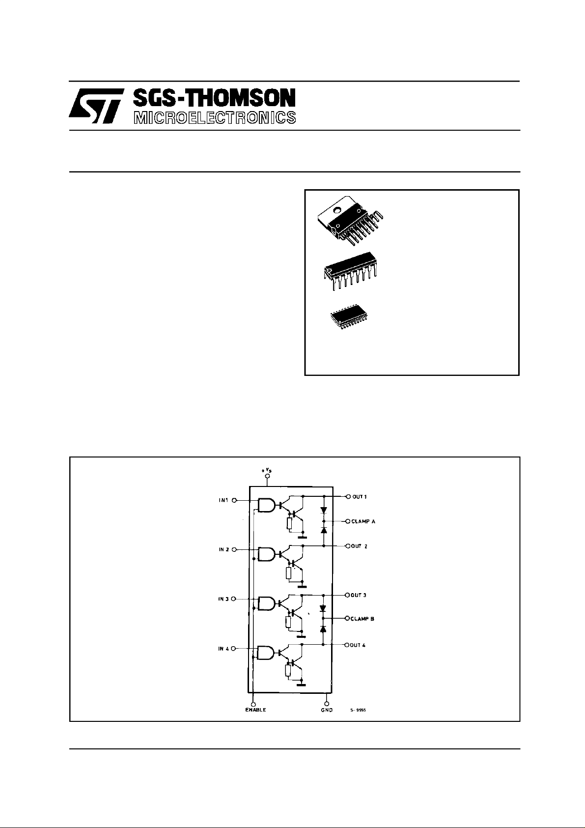
QUADDARLINGTON SWITCH
Multiwatt15
Powerdip12 + 2 + 2
DESCRIPTION
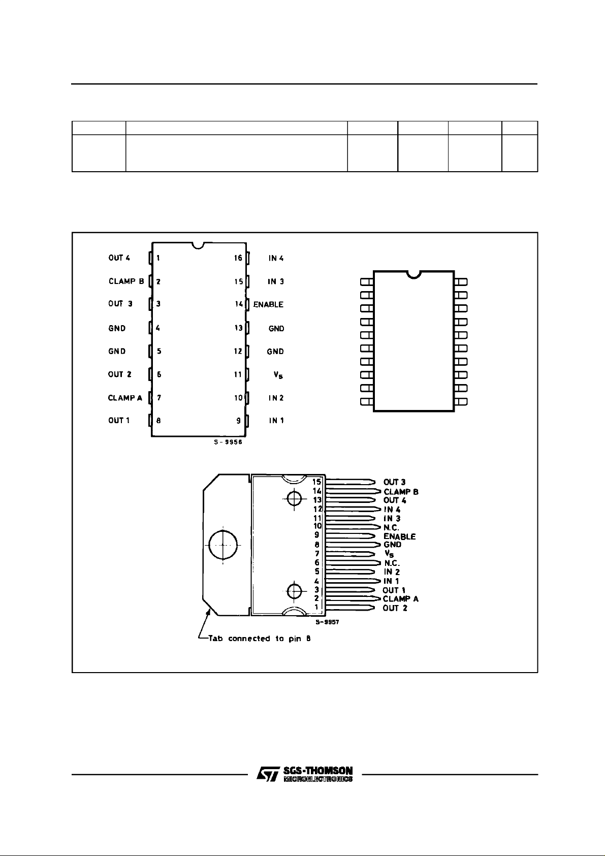
TheL6221monolithicquad darlingtonswitch isdesignedforhighcurrent,highvoltageswitchingapplications.Eachof the four switchesiscontrolledby a
logicinput and all fourare controlledby a common
enableinput.AllinputsareTTL-compatiblefordirect
connectionto logiccircuits.
Eachswitchconsistsofan open-collectordarlington
transistorplusafastdiodeforswitchingapplications
withinductivedeviceloads.Theemittersofthefourswitchesarecommoned.Any numberof inputsand
BLOCK DIAGRAM
SO16 + 2 + 2
ORDERING NUMBERS :L6221C (Powerdip12+2+2)
L6221CN (Multiwatt15 )
L6221CD (SO16+2+2)
outputsofthe same devicemay be paralleled.
Threeversionsare available: theL6221Cmounted
ina Powerdip12+ 2 +2 packageandthe L6221CN
mounted in a 15--lead Multiwatt package, the
L6221CDin SO16+2+2package.
May 1997
1/15
L6221C-L6221CN-L6221CD
THERMAL DATA
Symbol Parameter SO20 Powerdip Multiwatt15 Unit
R
th j-pins
R
th j-case
R
th j-amb
Thermal Resistance Junction-pins Max.
Thermal Resistance Junction-case Max.
Thermal Resistance Junction-ambient Max.
PIN CONNECTI ONS (top views)
17
80
14
–
–
80
–
3
35
C/W
°
°C/W
C/W
°
L6221C (Powerdip)
OUT4
CLAMPB
N.C.
OUT3
GND
GND
OUT2
N.C.
CLAMPA IN2
OUT1 IN1
2
3
4
5
6
7
8
9
10
D95IN231
20
19
18
17
16
15
14
13
12
11
IN41
IN3
N.C.
ENABLE
GND
GND
V
N.C.
L6221CD (SO20)
S
2/15
L6221CN (Multiwatt-15)
L6221 C-L6 221CN -L622 1CD
ABSOLUTEMAXIMUM RATINGS
Symbol Parameter Value Unit
V
V
V
IN,VEN
I
I
I
T
T
I
sub
P
Output Voltage 60 V
O
Logic Supply Voltage 7 V
S
Input Voltage, Enable Voltage V
Continuous Colllector Current (for each channel)
C
for L6221CD
Collector Peak Current (repetitive, duty cycle = 10% ton = 5ms)
C
for L6221CD
Collector Peak Current (non repetitive, t = 10µs)
C
for L6221CD
Operating Temperature Range (junction) -40 to +150
op
Storage Temperature Range -55 to +150
stg
S
1.8
1.2
2.5
1.7
3.2
2.2
Output Substrate Current 350 mA
Total Power Dissipation
tot
=90°C (powerdip)
at T
pins
at T
at T
at T
at T
at T
=90°C (multiwatt)
case
=90°C (SO20)
case
=70°C (powerdip)
amb
=70°C (multiwatt)
amb
=70°C (SO20)
amb
4.3
20
3.5
1
2.3
1
A
A
A
A
A
A
C
°
C
°
W
W
W
W
W
W
TRUTHTABLE
Enable Input Power Out
H
H
L
For each input : H = High level
L = Low level
X = Don’t care
H
L
X
PIN FUNCTIONS(seeblock diagram)
Name Function
IN 1 Input to Driver 1
IN 2 Input to Driver 2
OUT 1 Output of Driver 1
OUT 2 Output of Driver 2
CLAMP A Diode Clamp to Driver 1 and Driver 2
IN 3 Input to Driver 3
IN 4 Input to Driver 4
OUT 3 Output of Driver 3
OUT 4 Output of Driver 4
CLAMP B Diode Clamp to Driver3 and Driver 4
ENABLE Enable Input to All Drivers
VS Logic Supply Voltage
GND Common Ground
ON
OFF
OFF
3/15
L6221C-L6221CN-L6221CD
ELECTRICALCHARACTERISTICSReferto TheTestCircuittoFig.1to Fig.9(VS=5V,T
=25°Cunless
amb
otherwisespecified)
Symbol Parameter Test Condition Min. Typ. Max. Unit
V
I
I
CEX
V
CE(sat)
L, VENL Input Low Voltage 0.8 V
V
IN
L, IENL Input Low Current VIN=VINLVEN=VENL -100
I
IN
H, VENH Input High Voltage 2 V
V
IN
H, IENH Input High Current VIN=VINHVEN=VENH 100
I
IN
I
V
t
d(on)
t
d(off)
∆
Logic Supply Voltage 4.5 5.5 V
S
Logic Supply Current All outputs ON IC= 0.7A
S
All outputs OFF
Output Leakage Current VCE= 60V VEN=VENH
V
Collector Emitter Saturation Voltage
VS= 4.5V VIN=VINH
V
(one input on; all others inputs off).
Clamp Diode Leakage Current VR= 60V VEN=VENH
R
V
Clamp Diode Forward Voltage IF=1A
F
Turn on Delay Time
Turn off Delay Time
Logic Supply Current Variation VIN=5V VEN=5V
I
S
I
F
V
V
I
out
L
IN=VIN
EN=VEN
H
(*) I
L
IN=VIN
= 2A (*)
=5V RL=10
P
=5V RL=10
P
= -500mA for Each
Ω
Ω
I
C
C
=1A
=2A
Channel
20
20
1mA
1.4
1.85
100
1.8
2.2
2ms
5
150 mA
mA
mA
V
V
µ
µA
µ
V
V
µ
A
A
s
(*) Only for L6221C- L6221CN types
4/15
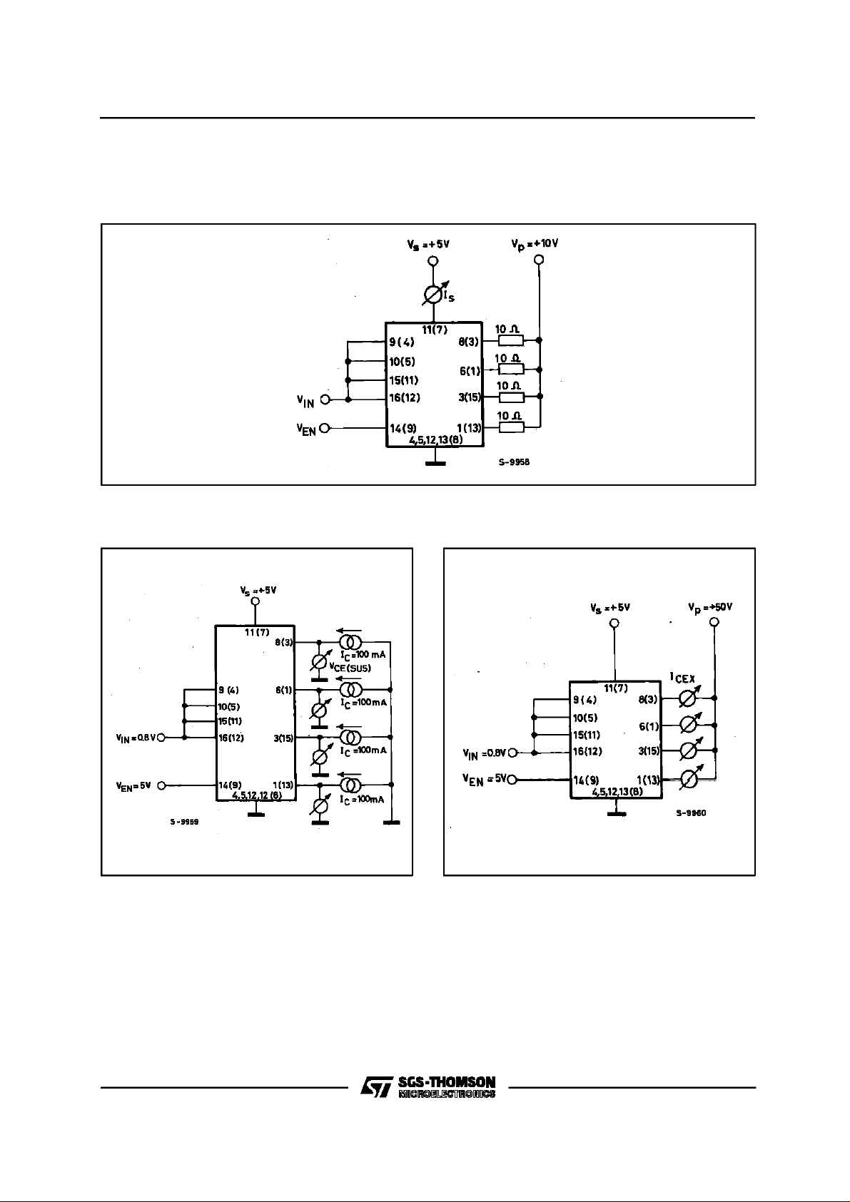
TEST CIRCUITS
(X)= Referredto Multiwatt package
X =Referredto Powerdippackage
Figure 1 : Lo gic s upply current.
SetVIN= 4.5V,VEN=0.8V, orVIN=0.8V, VEN= 4.5V,for IS(alloutputs off)
= 2V,VEN=2V, for IS(all outputson)
S
etVIN
L6221 C-L6 221CN -L622 1CD
Figure 2 :
Output Sustaining Volta ge.
Figure 3 :
Output Leaka ge Current
V
= +60V
P
.
5/15

L6221C-L6221CN-L6221CD
Figure4:Collector-emitter Saturation
Voltage.
Figure6:
Clamp Diode Leakage Current
Figure 5 : L ogic Inpu t Ch aracteristics.
SetS1,S2open,VIN,VEN= 0.8V for IINL, IENL
S
S
S
open, VIN,VEN=2V for IINH, IENH
etS1,S2
close,VIN,VEN= 0.8Vfor VINL,VENL
etS1,S2
close,VIN,VEN= 2Vfor VINH, VENH
etS1,S2
. Figure 7 :
Clamp Diode Forward Voltage.
6/15
V
P
= +60V

L6221 C-L6 221CN -L622 1CD
Figure 8 : Switch ing T ime s Te st Circuit. Figure9:Swit chin g TImes Wavefo rms.
Figure 10 : Allowe d Pe a k Collecto r Cu r-
rent vs. Duty Cycle for 1, 2, 3
or 4 Conte mporary Working
Outputs (L62 21C)
.
Figure 11 : Allowed Peak Collector Current
vs. Duty Cycle for 1, 2, 3 or 4
Contemporary Working Outputs
(L6221CN).
7/15

L6221C-L6221CN-L6221CD
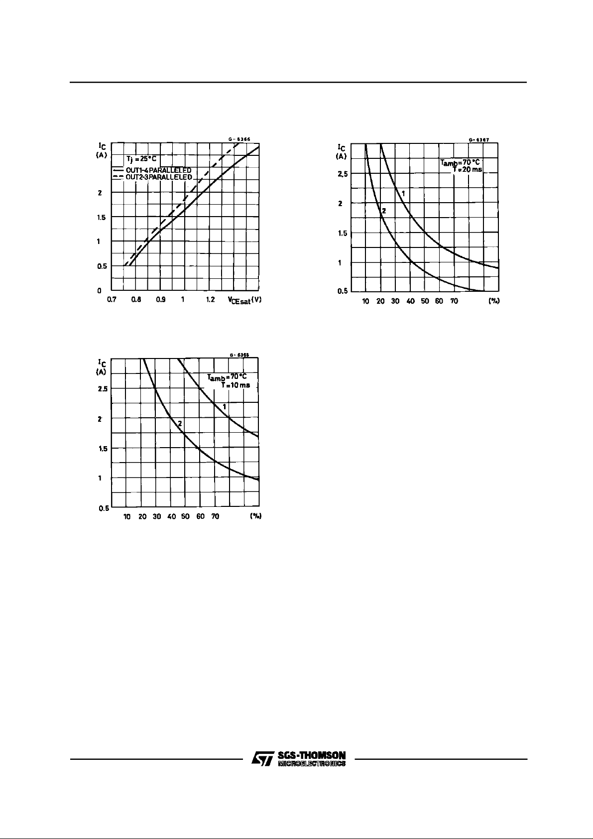
Figure 12 : Collector Saturation Voltage
vs. Collector C urrent.
Figure 14 : Collector Satu ration Voltage
vs. Junction Temperature
=1A.
at I
C
Figure 13 : F ree-wheeling Diode Fo rward
Voltage vs. Diode Current
.
Figure 15 : F ree-wheeling Diode Fo rward
Voltage vs. Junction Temperature at IF=1A
.
Figure 16 : Saturation Voltage vs. Junc-
tion Temperature at IC = 1.8A.
8/15
Figure 17 : F ree-wheeling Diode Fo rward
Voltage vs. Junction Temperature at If = 1.8A .

L6221 C-L6 221CN -L622 1CD
Figure 18.
Figure 19 : Driver for S olenoids u p to 3A.
APPL ICATION INFO RMATION
Wheninductive loads are drivenby L6221C/CD,a
zenerdiodein serieswiththeintegralfree-wheeling
diodes increases the voltage across whichenergy
stored in the load is discharged and therefore
speedsthecurrent decay(fig. 18).
The zener has to be chosen in such a way that
V
zener’svoltagechangesdueto:spreadonV
is limited to 60V taking into account the
CLAMP
,tem-
Z
peraturechanges,and the voltagedrop due to ohmicresistance.
Moreover,the instantaneouspowermustbe limited
in order to avoidthe reversesecondbreakdown.
Somecaremustbe takento ensurethatthe collectorsare placedclosetogetherto avoiddifferentcurrentpartitioningat turn-off.
We suggest to put in parallel channel 1 and 4 and
channel2 and3 as shownin figure19forthesimilar
electricalcharacteristicsofthelogicsection(turn-on
and turn-offdelay time) and the power stages(collector saturation voltage, free-wheeling diode forward voltage).
9/15
L6221C-L6221CN-L6221CD
Figure 20 : Saturation Voltage vs.
Collector Current.
Figure 22 : Pe ak Collector Current v s.
Duty Cycle for 1 or 2 Paralleled
Outputs Driven (L6221 CN).
Figure 21 : Pe ak Collector Current vs.
DutyCyclefor1or2Paralleled
Outputs Driven (L6221N).
10/15

MOUNTING INSTRUCTI ON
TheR
of the L6221Ccan be reducedby sol-
th j-amb
deringtheGNDpinstoa suitablecopperareaof the
printed circuit board (Fig. 23) or to an external
heatsink(Fig. 24).
Thediagram of figure25 showsthe maximumdissipablepowerP
andthe R
tot
thj-amb
asa functionof
theside” α” oftwo equalsquarecopperareashav-
L6221 C-L6 221CN -L622 1CD
ing a thicknessof 35µ (1.4mils). During soldering
the pins temperaturemust not exceed 260 °C and
the solderingtime mustnot be longer than 12 seconds.
The externalheatsinkor printedcircuitcopper area
must be connectedto electricalground.
Figure 23 :
Example of P.C. Board Copper
Area Which is Used as Heatsink.
Figure 25 : M aximum Dissipable Po we r
and Junction to Ambient Thermal Resistance vs. Si de ” α”
Figure 24 :
External Heatsink Mount ing
Example.
Figure 26 : Maximum Allowable Power
Dissipation vs. Ambient
.
Temperature.
11/15

L6221C-L6221CN-L6221CD
MULTIWATT15 PACKAGE MECHANICAL DATA
DIM. mm inch
MIN. TYP. MAX. MIN. TYP. MAX.
A 5 0.197
B 2.65 0.104
C 1.6 0.063
D 1 0.039
E 0.49 0.55 0.019 0.022
F 0.66 0.75 0.026 0.030
G 1.14 1.27 1.4 0.045 0.050 0.055
G1 17.57 17.78 17.91 0.692 0.700 0.705
H1 19.6 0.772
H2 20.2 0.795
L 22.1 22.6 0.870 0.890
L1 22 22.5 0.866 0.886
L2 17.65 18.1 0.695 0.713
L3 17.25 17.5 17.75 0.679 0.689 0.699
L4 10.3 10.7 10.9 0.406 0.421 0.429
L7 2.65 2.9 0.104 0.114
M 4.2 4.3 4.6 0.165 0.169 0.181
M1 4.5 5.08 5.3 0.177 0.200 0.209
S 1.9 2.6 0.075 0.102
S1 1.9 2.6 0.075 0.102
Dia1 3.65 3.85 0.144 0.152
12/15

L6221 C-L6 221CN -L622 1CD
POWERDIP16 PACKAGE MECHANICAL DATA
DIM. mm inch
MIN. TYP. MAX. MIN. TYP. MAX.
a1 0.51 0.020
B 0.85 1.40 0.033 0.055
b 0.50 0.020
b1 0.38 0.50 0.015 0.020
D 20.0 0.787
E 8.80 0.346
e 2.54 0.100
e3 17.78 0.700
F 7.10 0.280
I 5.10 0.201
L 3.30 0.130
Z 1.27 0.050
13/15

L6221C-L6221CN-L6221CD
SO20 PACKAGE MECHANICAL DATA
DIM. mm inch
MIN. TYP. MAX. MIN. TYP. MAX.
A 2.65 0.104
a1 0.1 0.3 0.004 0.012
a2 2.45 0.096
b 0.35 0.49 0.014 0.019
b1 0.23 0.32 0.009 0.013
C 0.5 0.020
c1 45 (typ.)
D 12.6 13.0 0.496 0.512
E 10 10.65 0.394 0.419
e 1.27 0.050
e3 11.43 0.450
F 7.4 7.6 0.291 0.299
L 0.5 1.27 0.020 0.050
M 0.75 0.030
S 8 (max.)
14/15

L6221 C-L6 221CN -L622 1CD
Information furnished is believed to be accurate and reliable. However, SGS-THOMSON Microelectronics assumes no responsibility for
the consequences of use of such information nor for any infringement of patents or other rights of third parties which may result from its
use. No license is granted by implication or otherwiseunder any patent or patent rights of SGS-THOMSON Microelectronics. Specification
mentioned in this publication are subject to change without notice. This publication supersedes and replaces all information previously
supplied. SGS-THOMSON Microelectronics products are not authorized for use as critical components in life support devices or systems
withoutexpress written approval of SGS-THOMSON Microelectronics.
Australia - Brazil- Canada - China - France - Germany - Hong Kong - Italy - Japan - Korea - Malaysia - Malta - Morocco -
The Netherlands - Singapore - Spain - Sweden - Switzerland - Taiwan - Thailand - United Kingdom - U.S.A.
1997 SGS-THOMSON Microelectronics – Printed in Italy – All Rights Reserved
SGS-THOMSON Microelectronics GROUP OF COMPANIES
15/15
 Loading...