

L6 221A L62 21 AD
.
FOURNONINVERTINGINPUTSWITH
ENABLE
.OUTPUT VOLTAGEUPTO50V
.OUTPUT CURRENT UPTO1.8A
.VERYLOW SATURATIONVOLTAGE
.
TTLCOMPATIBLEINPUTS
.INTEGRALFAST RECIRCULATIONDIODES
DESCRIP TION
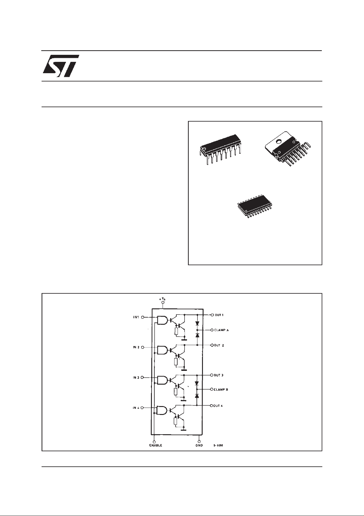
TheL6221monolithicquaddarlington switchis designedforhighcurrent,highvoltageswitchingapplications.Eachof thefourswitchesis controlledby a
logicinput and allfourare controlledby a common
enableinput.AllinputsareTTL-compatiblefordirect
connectiontologic circuits.
Eachswitchconsistsofanopen-collectordarlington
transistorplusafastdiodeforswitchingapplications
withinductivedeviceloads.The emittersof thefour
switchesare commoned.Anynumberofinputsand
outputsof the samedevice maybe paralleled.
L6221N
QUADDARLINGTON SWITCH
Powerdip12 +2 +2
SO16+2+2
ORDERINGNUMBERS:
L6221A(Powerdip)
L6221N (Multiwatt15)
L6221AD (SO16+2+2)
Multiwatt15
BLOCK DIAGRAM
July 1998
1/15

L6221A - L6221AD - L6221N
THERMAL DATA
Symbol Parameter SO20 Powerdip Multiwatt15 Unit
R
th j-pins
R
th j-case
R
th j-amb
Thermal Resistance Junction-pins Max.
Thermal Resistance Junction-case Max.
Thermal Resistance Junction-ambient Max.
17
80
–
–
80
14
–
3
35
C/W
°
C/W
°
C/W
°
PIN CO NNECTI ONS
L6221A (Powerdip)
(top vie ws)
CLAMPB
CLAMPA IN2
L6221N (Multiwatt-15)
L6221AD (SO16+2+2)
OUT4
2
N.C.
OUT3
GND
GND
OUT2
N.C.
OUT1 IN1
3
4
5
6
7
8
9
10
D95IN231
20
19
18
17
16
15
14
13
12
11
IN41
IN3
N.C.
ENABLE
GND
GND
V
N.C.
S
2/15
L6221A - L6221AD - L6221N
ABSOLUTE MAXIMUM RATINGS
Symbol Parameter Value Unit
V
V
V
IN,VEN
I
I
I
T
T
I
sub
P
o
s
C
C
C
op
stg
tot
Output Voltage 50 V
Logic Supply Voltage 7 V
Input Voltage, Enable Voltage V
s
Continuous Collector Current (for each channel) 1.8 A
Collector Peak Current (repetitive, duty cycle = 10 % ton= 5 ms) 2.5 A
Collector Peak Current (non repetitive, t = 10µs)
3.2 A
Operating Temperature Range (junction) – 40 to + 150
Storage Temperature Range – 55 to + 150
Output Substrate Current 350 mA
Total Power Dissipation at T
at T
at T
at T
at T
at T
=90°C (powerdip)
pins
=90°C (multiwatt)
case
=90°C (SO20)
case
=70°C (powerdip)
amb
=70°C (multiwatt)
amb
=70°C (SO20)
amb
4.3
20
3.5
1
2.3
1
°C
°
W
W
W
W
W
W
C
TRUTH TABLE
Enable Input Power Out
H
H
L
Foreach input: H = Highlevel
L = Low level
H
L
X
PIN FUNCTIONS (see block diagram)
Name Function
IN 1 Input to Driver 1
IN 2 Input to Driver 2
OUT 1 Output of Driver 1
OUT 2 Output of Driver 2
CLAMP A Diode Clamp to Driver 1 and Driver 2
IN 3 Input to Driver 3
IN 4 Input to Driver 4
OUT 3 Output of Driver 3
OUT 4 Output of Driver 4
CLAMP B Diode Clamp to Driver 3 and Driver 4
ENABLE Enable Input to All Drivers
V
S
GND Common Ground
Logic Supply Voltage
ON
OFF
OFF
3/15
L6221A - L6221AD - L6221N
ELECTRICAL CHARACTERISTICS
Refer to the test circuit to Fig. 1 to Fig. 9 (V
= 5V, T
S
Symbol Parameter Test Conditions Min . Typ . Max . Unit
V
S
I
s
V
CE(sus)
I
CEX
V
CE(sat)
L, VENL Input Low Voltage 0.8 V
V
IN
L, IENL Input Low Current VIN=VINL, VEN=VENL – 100
I
IN
L, VENH Input High Voltage 2.0 V
V
IN
H,IENH Input High Current VIN=VINH, VEN=VENH
I
IN
I
R
V
F
t
d (on)
t
d (off)
I
∆
Logic Supply Voltage 4.5 5.5 V
Logic Supply Current All Outputs ON, IC= 0.7A
All Outputs OFF
Output Sustaining Voltage VIN=VINL, VEN=VENH
= 100 mA
I
C
Output Leakage Current VCE= 50V
V
IN=VIN
Collector Emitter Saturation Voltage
(one input on ; all others inputs off.)
Vs= 4.5V
V
IN=VIN
= 0.6A
I
C
=1A
I
C
= 1.8A
I
C
Clamp Diode Leakage Current VR=50V,VEN=VENH
V
IN=VIN
Clamp Diode Forward Voltage IF=1A
= 1.8A
I
F
Turn on Delay Time
Turn off DelayTime
Logic Supply Current Variation VIN= 5V, VEN=5V
s
= 5V, RL=10
V
p
= 5V, RL=10Ω
V
p
= – 300mA for Each Channel
I
out
=25oC unless otherwise specified)
amb
46 V
L, VEN=VENH
H, VEN=VENH
L
Ω 2 µ
2020mA
1mA
1
1.2
1.6
10
±
100 µ
1.6
2.0VV
5
120 m A
mA
V
µ
µ
µs
A
A
A
s
4/15
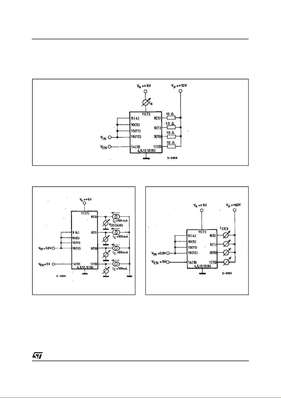
TEST CIR CUITS
(X)= Referredto Multiwattpackage
X = Referredto Powerdippackage
Figure 1 : Logic supply current.
SetVIN= 4.5V,VEN= 0.8V,or VIN= 0.8V,VEN=4.5V, for IS(alloutputs off)
S
= 2V, VEN= 2V, for IS(alloutputson)
etVIN
L6221A - L6221AD - L6221N
Figure 2 : Output SustainingVoltage. Figur e 3 : Output Leakage Current.
5/15

L6221A - L6221AD - L6221N
Figure 4 : Collector-emitter Saturation
Figure 5 : Logic InputCharacteristics
Voltage
SetS1,S2open,VIN,VEN= 0.8Vfor IINL,IENL
S
S
S
open, VIN,VEN= 2V for IINH, IENH
etS1,S2
close,VIN,VEN= 0.8V forVINL,VENL
etS1,S2
close,VIN,VEN= 2V for VINH,VENH
etS1,S2
Figure 6 : Clamp Diode Le akage Current. Figure7:Clamp Diode Forward Voltage.
6/15

L6221A - L6221AD - L6221N
Figure 8 : Switch in g T ime s Test Cir cu it. Figure9:Switch i ng TIme s Wave form s.
Figure 10 : AllowedPeakCollectorCurrentver-
susDutyCyclefor 1,2, 3 or4 ContemporaryWorking Outputs(L6221A)
Figure 11 : AllowedPeakCollector Currentver-
susDutyCyclefor 1, 2, 3 or 4 ContemporaryWorking Outputs
(L6221N)
7/15

L6221A - L6221AD - L6221N
Figure 12 : CollectorSaturationVoltageversus
Collector Current
Figure 14 :
CollectorSaturationVoltageversus
JunctionTemperatureat IC =1A
Figure 13 : Free-wheelingDiode ForwardVoltage
versusDiodeCurrent
Figure 15 :
Free-wheelingDiodeForwardVoltage
versusJunctionTemperature
at IF= 1A
Figure 16 :
8/15
Saturation Voltage vs. Junc-
Figure 17 :
Free-wheeling Diode Forward

L6221A - L6221AD - L6221N
APPLICATION INFORMATION
When inductive loads are driven by L6221A/N, a
zenerdiodeinseries withtheintegralfree-wheeling
diodesincreasesthe voltage across which energy
stored in the load is discharged and therefore
speedsthe currentdecay(fig. 18).
Forreliabilityitissuggestedthatthezenerischosen
sothat V
p+Vz
<35V.
Thereasonsfor this are two fold :
1) The zener voltage changesin temperatureand
current.
2)Theinstantaneouspowermustbelimitedtoavoid
thereverse secondbreakdown.
Figure 19 :
Driver f or Solenoids up to 3A
.
Figure 18.
Somecare mustbe taken to ensurethatthe collectorsareplacedclosetogethertoavoiddifferentcurrentpartitioningat turn-off.
We suggest to put in parallel channel1 and 4 and
channel2and3 asshowninfigure19 forthesimilar
electricalcharacteristicsofthelogicsection(turn-on
and turn-offdelay time) andthe power stages(collector saturation voltage, free-wheeling diode forward voltage).
9/15

L6221A - L6221AD - L6221N
Figure 20 : SaturationVoltageversusCollector
Current
Figure 22 : PeakCollector CurrentversusDuty
Cyclefor 1 or 2 ParalleledOutputs
Driven(L6221N)
Figure 21 : Peak CollectorCurrentversusDuty
Cyclefor 1 or 2 ParalleledOutputs
Driven(L6221A)
10/15

MOUNTING INS TRUCT I ON
TheR
of the L6221Acan be reduced by sol-
th j-amb
deringtheGNDpinsto asuitablecopperareaofthe
printed circuit board (Fig. 23) or to an external
heatsink(Fig.24).
Thediagramof figure25 showsthe maximum dissipablepower P
andtheR
tot
th j-amb
asa functionof
theside ” α” of twoequalsquarecopperareashav-
WhichisUsed as Heatsink
L6221A - L6221AD - L6221N
ing a thicknessof 35µ (1.4mils). During soldering
the pins temperaturemust not exceed 260 °C and
the solderingtime mustnot belonger than12 seconds.
Theexternalheatsinkor printedcircuitcopperarea
mustbeconnectedto electricalground.
Figure 24 : ExternalHeatsinkMountingExampleFigure 23 : Exampleof P.C. BoardCopperArea
Figure 25 : MaximumDissipable Powerand Junc-
tionto AmbientThermalResistance
versusSide ” α”
Figure 26 : MaximumAllowablePowerDissipa-
tionversusAmbientTemperature
11/15

L6221A - L6221AD - L6221N
POWERDIP 16 PACKAGE MECHANICAL DATA
DIM.
MIN. TYP. MAX. MIN. TYP. MAX.
a1 0.51 0.020
B 0.85 1.40 0.033 0.055
b 0.50 0.020
b1 0.38 0.50 0.015 0.020
D 20.0 0.787
E 8.80 0.346
e 2.54 0.100
e3 17.78 0.700
F 7.10 0.280
I 5.10 0.201
L 3.30 0.130
Z 1.27 0.050
mm inch
12/15

MULTIWATT 15 PACKAGE MECHANICAL DATA
L6221A - L6221AD - L6221N
DIM.
MIN. TYP. MAX. MIN. TYP. MAX.
A 5 0.197
B 2.65 0.104
C 1.6 0.063
D 1 0.039
E 0.49 0.55 0.019 0.022
F 0.66 0.75 0.026 0.030
G 1.02 1.27 1.52 0.040 0.050 0.060
G1 17.53 17.78 18.03 0.690 0.700 0.710
H1 19.6 0.772
H2 20.2 0.795
L 21.9 22.2 22.5 0.862 0.874 0.886
L1 21.7 22.1 22.5 0.854 0.870 0.886
L2 17.65 18.1 0.695 0.713
L3 17.25 17.5 17.75 0.679 0.689 0.699
L4 10.3 10.7 10.9 0.406 0.421 0.429
L7 2.65 2.9 0.104 0.114
M 4.25 4.55 4.85 0.167 0.179 0.191
M1 4.63 5.08 5.53 0.182 0.200 0.218
S 1.9 2.6 0.075 0.102
S1 1.9 2.6 0.075 0.102
Dia1 3.65 3.85 0.144 0.152
mm inch
13/15

L6221A - L6221AD - L6221N
SO20 PACKAGE MECHANICAL DATA
DIM.
MIN. TYP. MAX. MIN. TYP. MAX.
A 2.35 2.65 0.093 0.104
A1 0.1 0.3 0.004 0.012
B 0.33 0.51 0.013 0.020
C 0.23 0.32 0.009 0.013
D 12.6 13 0.496 0.512
E 7.4 7.6 0.291 0.299
e 1.27 0.050
H 10 10.65 0.394 0.419
h 0.25 0.75 0.010 0.030
L 0.4 1.27 0.016 0.050
K 0 (min.)8 (max.)
mm inch
L
A
B
e
K
D
1120
E
110
hx45°
SO20MEC
A1
C
H
14/15

L6221A - L6221AD - L6221N
Information furnished is believed to be accurate and reliable. However, STMicroelectronics assumes no responsibility for the consequences of use of such information nor for any infringement of patents or other rights of third parties which may result from its use. No
license is granted by implication or otherwise under any patent or patent rights of STMicroelectronics. Specification mentioned in this
publication are subject to change without notice. This publication supersedes and replaces all information previously supplied. STMicroelectronics products are not authorized for use as critical components in life support devices or systems without express written
approval of STMicroelectronics.
Australia - Brazil - Canada - China- France - Germany - Italy - Japan - Korea - Malaysia - Malta - Mexico - Morocco - The Netherlands -
Singapore - Spain - Sweden - Switzerland - Taiwan - Thailand - United Kingdom- U.S.A.
The ST logo is a registered trademark of STMicroelectronics
1998 STMicroelectronics – Printed in Italy –All RightsReserved
STMicroelectronics GROUP OF COMPANIES
15/15
 Loading...