

.TWONON INVERTING+TWOINVERTINGIN-
PUTS WITHINHIBIT
.OUTPUTVOLTAGEUP TO 50V
.OUTPUTCURRENT UP TO 1.8A
.VERYLOW SATURATIONVOLTAGE
.TTLCOMPATIBLEINPUTS
.INTEGRALFAST RECIRCULATIONDIODES
DESCRIP TION
TheL6220monolithicquaddarlingtonswitchis designedforhighcurrent,highvoltageswitchingapplications.Eachofthefour switchesis controlledby a
logicinput and all four are controlledby a common
inhibitinput.AllinputsareTTL-compatiblefor direct
connectiontologic circuits.
Eachswitchconsistsofanopen-collectordarlington
transistorplusafastdiodeforswitchingapplications
with inductive loads. The emitters of the four
switchesarecommoned.Anynumberof inputsand
outputsof thesamedevice may be paralleled.
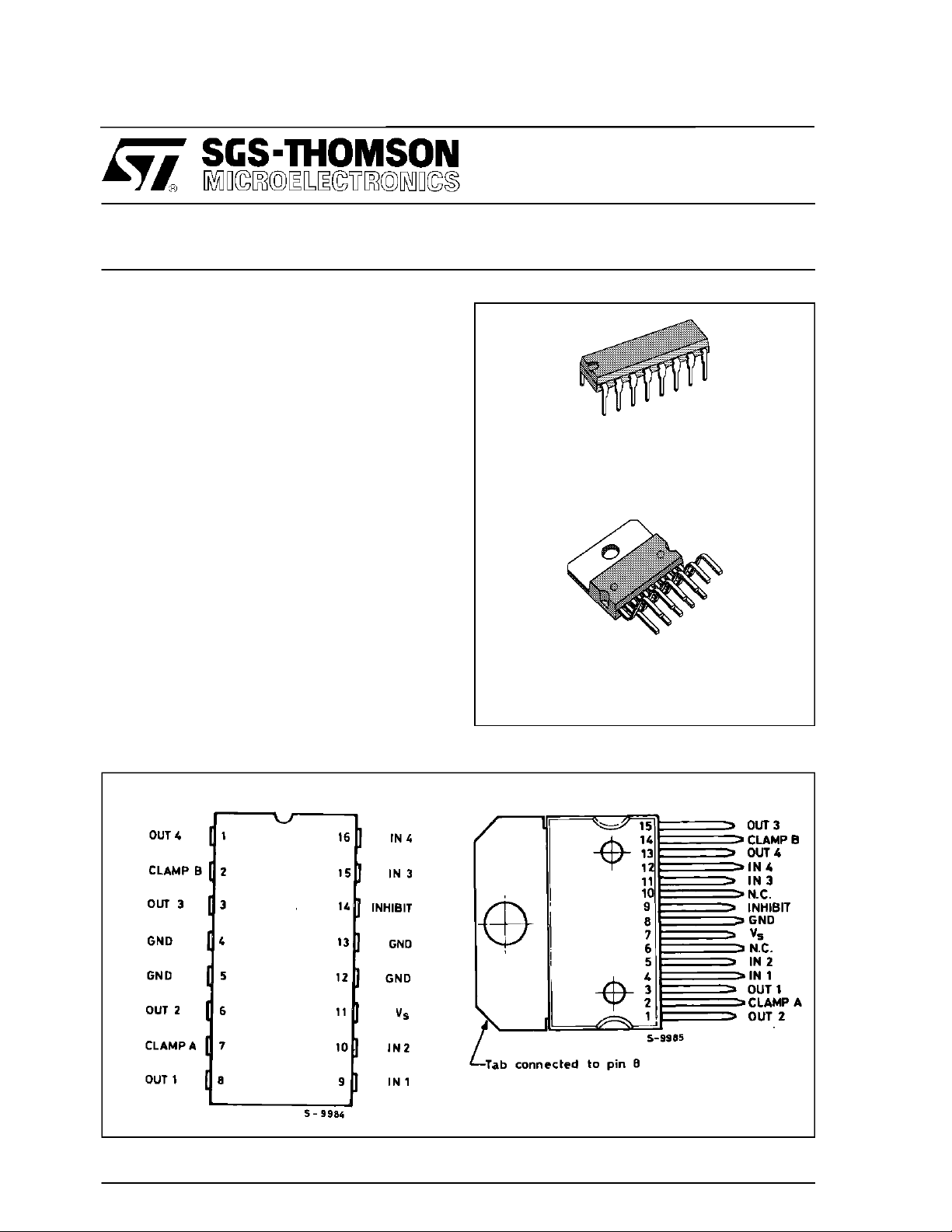
Two versionsare available: theL6220 mountedin
a Powerdip 12 + 2 + 2 packageand the L6220N
mountedin a 15-leadMultiwattpackage.
L6220
L6220N
QUAD DARLINGTON SWITCHES
Powerdip 12 + 2 + 2
(PlasticPackage)
ORDERING NUMBER : L6220
Multiwatt15
(PlasticPackage)
ORDERING NUMBER : L6220N
PIN CONNECTIO NS (top vie ws)
L6220 (Powerdip) L6220N (Multiwatt-15)
April1993
1/12

L6220 - L6220N
PIN FUNCTIONS (see block diagram)
Name Function
IN 1 Input to Driver 1
IN 2 Input to Driver 2
OUT 1 Output of Driver 1
OUT 2 Output of Driver 2
CLAMP A Diode Clamp to Driver 1 and Driver 2
IN 3 Input to Driver 3
IN 4 Input to Driver 4
OUT 3 Output of Driver 3
OUT 4 Output of Driver 4
CLAMP B Diode Clamp to Driver 3 and Driver 4
INHIBIT Inhibit Input to all Drivers
V
s
GND Common Ground
BLOCK DIAG RAM
Logic Supply Voltage
TRUTH TABLE
Inhibit Input 1, 4 Power Out Inhibit Inputs 2, 3 Power Out
L
L
H
Foreach input : H = High level
L = Low level
2/12
H
L
X
ON
OFF
OFF
L
L
H
L
H
X
ON
OFF
OFF
L6220 - L6220N
ABSOLUTE MAXIMUM RATINGS
Symbol Parameter Value Unit
V
o
V
s
V
IN,VINH
I
C
I
C
I
C
T
op
T
stg
I
sub
P
tot
THERMAL DATA
Symbol Parameter Powerdip Multiwatt–15 Unit
R
th j-pins
R
th j-case
R
th j-amb
Ouput Voltage 50 V
Logic SupplyVoltage 7 V
Input Voltage, Inhibit Voltage V
s
Continuous Collector Current (for each channel) 1.8 A
Collector Peak Current (repetitive, duty cycle = 10 % ton= 5 ms) 2.5 A
Collector Peak Current (non repetitive, t = 10 µs) 3.2 A
Operating Temperature Range (junction) – 40 to + 150 °C
Storage Temperature Range – 55 to + 150 °C
Output Substrate Current 350 mA
Total Power Dissipation at T
at T
at T
at T
=90oC (Powerdip)
pins
=90oC (Multiwatt)
case
=70oC (Powerdip)
amb
=70oC (Multiwatt)
amb
4.3
20
1
2.3
Thermal Resistance Junction-pins Max. 14 Thermal Resistance Junction-case Max. - 3
Thermal Resistance Junction-ambient Max. 80 35
o
C/W
o
C/W
o
C/W
W
W
W
W
ELECTRICAL CHARACTERISTICS
Refer to the testcircuits Fig. 1 to Fig.9 (V
= 5V, T
S
Symbol Parameter Test Conditions Min. Typ. Max. Unit
V
S
I
s
V
CE (sus)
I
CEX
V
CE (sat)
V
IN
V
INH
I
L, I
IN
H,
V
IN
V
INH
I
H, I
IN
I
R
V
F
t
d (on)
t
d (off)
∆I
Logic SupplyVoltage 4.5 5.5 V
Logic SupplyCurrent All Outputs ON, IC= 0.7A
All Outputs OFF
Output Sustaining Voltage IC=100mA, V
Output Leakage Current VCE= 50V, V
Collector Emitter Saturation Voltage
(one output on ; all others off.)
Input Low Voltage 0.8 V
L,
Vs= 4.5V, V
V
L
L Input Low Current VIN=VINL, V
INH
Input High Voltage 2.0 V
H
H Input High Current VIN=VINH, V
INH
Clamp Diode Leakage Current VR= 50V, V
Clamp Diode Forward Voltage IF=1A
I
F
Turn on Delay Time Vp= 5V, RL=10Ω 2 µs
Turn off Delay Time Vp= 5V, RL=10Ω 5 µs
Logic SupplyCurrent Variation VIN= 5V, VEN=5V
s
I
out
=25oC unless otherwise specified)
amb
H46 V
H1mA
L
L - 100 µA
H ± 10 µA
H 100 µA
INH=VINH
= 0.6A
I
C
=1A
I
C
= 1.8A
I
C
INH=VINH
IN 1.4=VINH
IN 2.3=VIN
L
INH=VINH
INH=VINH
INH=VINH
= 1.8A
= – 300mA for each Channel
2020mA
1
1.2
1.6
1.6
2.0VV
120 mA
MA
V
3/12
L6220 - L6220N
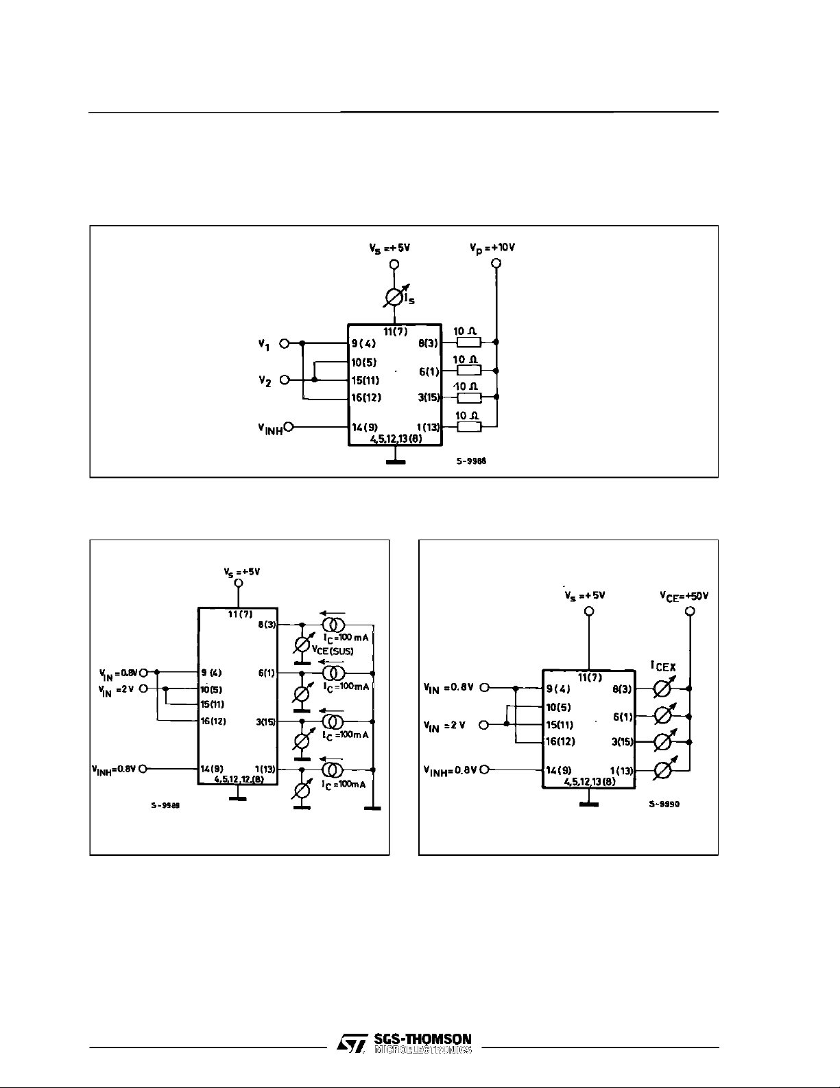
TEST CIRCUITS
(X) = Referred to Multiwatt package
X = Referredto Powerdippackage
Figure 1 : Lo gic Supply Current.
SetV1= 4.5V, V2= 0.8V, V
=2V, V2= 0.8V, V
SetV
1
=4.5VorV1= 0.8V,V2= 4.5V,V
INH
= 0.8V for IS(alloutputs on).
INH
=0.8 for IS(all outputs off).
INH
Figure 2 : Ou tput S ustaining Voltage. Figure 3 : Out put Leaka ge Current.
4/12

L6220 - L6220N
Figure 4 : Co llector-emit ter Sat u ra tion Figure 5 : Logic Input Characteristics.
Set S1,S2open, VIN,V
1,S2
1,S2
1,S2
open,VIN,V
close,VIN,V
close,VIN,V
Set S
Set S
Set S
= 0.8V for IINL,I
INH
= 2V for IINH, I
INH
= 0.8V for VINL,V
INH
=2V for VINH,V
INH
INH
INH
INH
H
INH
L
L
H.
Figure 6 : Clamp Diode Leakage Cu rrent. Figur e 7 : Clamp Diode Forward Vo ltage.
5/12

L6220 - L6220N
Figure 8 : S witching Times Te st Circ uit . Figure 9 : Switchi ng Times Wav eforms.
Figure 10 : Collector SaturationVoltageversus
Collector Current
Figure11 : Free-wheeling Diode ForwardVoltage
versusDiodeCurrent
6/12

L6220 - L6220N
Figure 12 : Collector SaturationVoltageversus
JunctionTemperatureat IC = 1A
Figure 14 : Collector SaturationVoltageversus
JunctionTemperatureat IC = 1.8A
Figure13 : Free-wheelingDiodeForwardVoltage
versusJunctionTemperature
at If =1A
Figure15 : Free-wheelingDiodeForwardVolt-
age versusJunctionTemperature
= 1.8A
at I
F
Figure 16.
Figure 1 7 : Unipolar Stepper Moto r Driver.
7/12

L6220 - L6220N
APPLICATION INFORMATION
When inductive loads are driven by L6220/N, a
zenerdiodeinserieswiththe integralfree-wheeling
diodesincreasesthe voltage across which energy
stored in the load is discharged and therefore
speedsthe current decay(Fig. 16). For reliability it
is suggested that the zeneris chosenso thatV
<35V.
V
z
Thereasonsfor this aretwofold :
1) The zenervoltage changesin temperature and
current.
p
2) The instantaneouspower mustbe limited to
avoid thereverse secondbreakdown.
Theparticularinternallogicallowsaneasierfullstep
drivingusingonly two input signals.
+
Figure 18 : AllowedPeak Collector-current versus
DutyCycle for 1, 2, 3 or 4 ContemporaryWorking Outputs(L6220).
MOUNTING INST RUCTIO N
TheR
oftheL6220canbereducedbysolder-
thj-amb
ing the GND pins to a suitablecopper area of the
printed circuit board (Fig. 20) or to an external
heatsink(Fig.21).
The diagram of figure 22 shows the maximum dissipablepowerP
and the R
tot
asa functionof
th j-amb
theside ” α” oftwo equalsquare copperareashav-
Figure19 : AllowedPeak CollectorCur-rent ver-
sus Duty Cyclefor 1, 2, 3 or 4 ContemporaryWorking Outputs
(L6220N).
ing a thicknessof 35µ (1.4 mils). Duringsoldering
the pinstemperaturemust not exceed 260 °C and
the solderingtime must not be longerthan 12 seconds.
Theexternalheatsinkor printed circuit copperarea
must be connectedto electrical ground.
8/12

L6220 - L6220N
Figure 20 : Exampleof P.C. Board Copperarea
whichis used as Heatsink
Figure 22 : Maximum DissipablePowerand Junc-
tion to AmbientThermal Resistance
versusSide”α”
Figure21 : ExternalHeatsinkMounting Example
Figure23 : MaximumAllowablePowerDissipa-
tionversusAmbient Temperature
9/12

L6220 - L6220N
MULTIWATT15 PACKAGE MECHANICAL DATA
DIM.
MIN. TYP. MAX. MIN. TYP. MAX.
A 5 0.197
B 2.65 0.104
C 1.6 0.063
D 1 0.039
E 0.49 0.55 0.019 0.022
F 0.66 0.75 0.026 0.030
G 1.14 1.27 1.4 0.045 0.050 0.055
G1 17.57 17.78 17.91 0.692 0.700 0.705
H1 19.6 0.772
H2 20.2 0.795
L 22.1 22.6 0.870 0.890
L1 22 22.5 0.866 0.886
L2 17.65 18.1 0.695 0.713
L3 17.25 17.5 17.75 0.679 0.689 0.699
L4 10.3 10.7 10.9 0.406 0.421 0.429
L7 2.65 2.9 0.104 0.114
M 4.2 4.3 4.6 0.165 0.169 0.181
M1 4.5 5.08 5.3 0.177 0.200 0.209
S 1.9 2.6 0.075 0.102
S1 1.9 2.6 0.075 0.102
Dia1 3.65 3.85 0.144 0.152
mm inch
10/12

POWERDIP16 PACKAGE MECHANICAL DATA
L6220 - L6220N
DIM.
MIN. TYP. MAX. MIN. TYP. MAX.
a1 0.51 0.020
B 0.85 1.40 0.033 0.055
b 0.50 0.020
b1 0.38 0.50 0.015 0.020
D 20.0 0.787
E 8.80 0.346
e 2.54 0.100
e3 17.78 0.700
F 7.10 0.280
I 5.10 0.201
L 3.30 0.130
mm inch
Z 1.27 0.050
11/12

L6220 - L6220N
Information furnished is believed to be accurate and reliable. However, SGS-THOMSON Microelectronics assumes no responsibility for
the consequences of use of such information nor for any infringement of patents or other rights of third parties which may result from its
use. No license is granted by implication or otherwise under any patent or patent rights of SGS-THOMSON Microelectronics. Specifications mentioned in this publication are subject to change without notice. This publication supersedes and replaces all information previously supplied. SGS-THOMSON Microelectronics products are not authorized for use as critical components in life support devices or
systems withoutexpress written approval of SGS-THOMSON Microelectronics.
1994 SGS-THOMSON Microelectronics - All Rights Reserved
Australia - Brazil - France- Germany - Hong Kong - Italy - Japan - Korea - Malaysia - Malta - Morocco - The Netherlands - Singapore -
SGS-THOMSON Microelectronics GROUPOF COMPANIES
Spain - Sweden - Switzerland - Taiwan - Thaliand - United Kingdom - U.S.A.
MULTIWATT isa Registered Trademark
12/12
 Loading...