

SGS Thomson Microelectronics L6220N, L6220 Datasheet
.TWONON INVERTING+TWOINVERTINGIN-
PUTS WITHINHIBIT
.OUTPUTVOLTAGEUP TO 50V
.OUTPUTCURRENT UP TO 1.8A
.VERYLOW SATURATIONVOLTAGE
.TTLCOMPATIBLEINPUTS
.INTEGRALFAST RECIRCULATIONDIODES
DESCRIP TION
TheL6220monolithicquaddarlingtonswitchis designedforhighcurrent,highvoltageswitchingapplications.Eachofthefour switchesis controlledby a
logicinput and all four are controlledby a common
inhibitinput.AllinputsareTTL-compatiblefor direct
connectiontologic circuits.
Eachswitchconsistsofanopen-collectordarlington
transistorplusafastdiodeforswitchingapplications
with inductive loads. The emitters of the four
switchesarecommoned.Anynumberof inputsand
outputsof thesamedevice may be paralleled.
Two versionsare available: theL6220 mountedin
a Powerdip 12 + 2 + 2 packageand the L6220N
mountedin a 15-leadMultiwattpackage.
L6220
L6220N
QUAD DARLINGTON SWITCHES
Powerdip 12 + 2 + 2
(PlasticPackage)
ORDERING NUMBER : L6220
Multiwatt15
(PlasticPackage)
ORDERING NUMBER : L6220N
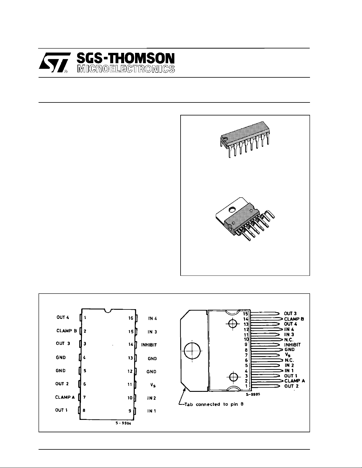
PIN CONNECTIO NS (top vie ws)
L6220 (Powerdip) L6220N (Multiwatt-15)
April1993
1/12

L6220 - L6220N
PIN FUNCTIONS (see block diagram)
Name Function
IN 1 Input to Driver 1
IN 2 Input to Driver 2
OUT 1 Output of Driver 1
OUT 2 Output of Driver 2
CLAMP A Diode Clamp to Driver 1 and Driver 2
IN 3 Input to Driver 3
IN 4 Input to Driver 4
OUT 3 Output of Driver 3
OUT 4 Output of Driver 4
CLAMP B Diode Clamp to Driver 3 and Driver 4
INHIBIT Inhibit Input to all Drivers
V
s
GND Common Ground
BLOCK DIAG RAM
Logic Supply Voltage
TRUTH TABLE
Inhibit Input 1, 4 Power Out Inhibit Inputs 2, 3 Power Out
L
L
H
Foreach input : H = High level
L = Low level
2/12
H
L
X
ON
OFF
OFF
L
L
H
L
H
X
ON
OFF
OFF
L6220 - L6220N
ABSOLUTE MAXIMUM RATINGS
Symbol Parameter Value Unit
V
o
V
s
V
IN,VINH
I
C
I
C
I
C
T
op
T
stg
I
sub
P
tot
THERMAL DATA
Symbol Parameter Powerdip Multiwatt–15 Unit
R
th j-pins
R
th j-case
R
th j-amb
Ouput Voltage 50 V
Logic SupplyVoltage 7 V
Input Voltage, Inhibit Voltage V
s
Continuous Collector Current (for each channel) 1.8 A
Collector Peak Current (repetitive, duty cycle = 10 % ton= 5 ms) 2.5 A
Collector Peak Current (non repetitive, t = 10 µs) 3.2 A
Operating Temperature Range (junction) – 40 to + 150 °C
Storage Temperature Range – 55 to + 150 °C
Output Substrate Current 350 mA
Total Power Dissipation at T
at T
at T
at T
=90oC (Powerdip)
pins
=90oC (Multiwatt)
case
=70oC (Powerdip)
amb
=70oC (Multiwatt)
amb
4.3
20
1
2.3
Thermal Resistance Junction-pins Max. 14 Thermal Resistance Junction-case Max. - 3
Thermal Resistance Junction-ambient Max. 80 35
o
C/W
o
C/W
o
C/W
W
W
W
W
ELECTRICAL CHARACTERISTICS
Refer to the testcircuits Fig. 1 to Fig.9 (V
= 5V, T
S
Symbol Parameter Test Conditions Min. Typ. Max. Unit
V
S
I
s
V
CE (sus)
I
CEX
V
CE (sat)
V
IN
V
INH
I
L, I
IN
H,
V
IN
V
INH
I
H, I
IN
I
R
V
F
t
d (on)
t
d (off)
∆I
Logic SupplyVoltage 4.5 5.5 V
Logic SupplyCurrent All Outputs ON, IC= 0.7A
All Outputs OFF
Output Sustaining Voltage IC=100mA, V
Output Leakage Current VCE= 50V, V
Collector Emitter Saturation Voltage
(one output on ; all others off.)
Input Low Voltage 0.8 V
L,
Vs= 4.5V, V
V
L
L Input Low Current VIN=VINL, V
INH
Input High Voltage 2.0 V
H
H Input High Current VIN=VINH, V
INH
Clamp Diode Leakage Current VR= 50V, V
Clamp Diode Forward Voltage IF=1A
I
F
Turn on Delay Time Vp= 5V, RL=10Ω 2 µs
Turn off Delay Time Vp= 5V, RL=10Ω 5 µs
Logic SupplyCurrent Variation VIN= 5V, VEN=5V
s
I
out
=25oC unless otherwise specified)
amb
H46 V
H1mA
L
L - 100 µA
H ± 10 µA
H 100 µA
INH=VINH
= 0.6A
I
C
=1A
I
C
= 1.8A
I
C
INH=VINH
IN 1.4=VINH
IN 2.3=VIN
L
INH=VINH
INH=VINH
INH=VINH
= 1.8A
= – 300mA for each Channel
2020mA
1
1.2
1.6
1.6
2.0VV
120 mA
MA
V
3/12
L6220 - L6220N
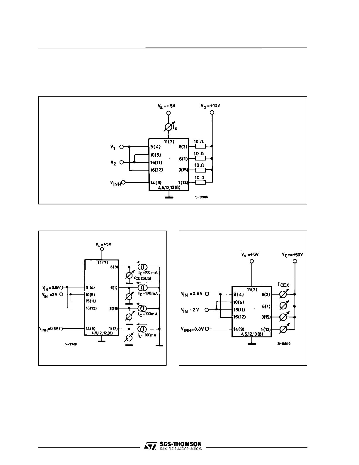
TEST CIRCUITS
(X) = Referred to Multiwatt package
X = Referredto Powerdippackage
Figure 1 : Lo gic Supply Current.
SetV1= 4.5V, V2= 0.8V, V
=2V, V2= 0.8V, V
SetV
1
=4.5VorV1= 0.8V,V2= 4.5V,V
INH
= 0.8V for IS(alloutputs on).
INH
=0.8 for IS(all outputs off).
INH
Figure 2 : Ou tput S ustaining Voltage. Figure 3 : Out put Leaka ge Current.
4/12
 Loading...