


STEPPER MOTOR DRIVER FOR AUTOMOTIVE RANGE
ABLE TO DRIVE BOTH WINDINGS OF BIPOLAR STEPPER MOTOR
OUTPUT CURRENT UP TO 750mA EACH
WINDING
WIDEVOLTAGERANGE 10V TO 46V
HALF-STEP, FULL-STEP AND MICROSTEPP-
INGMODE
BUILT-INPROTECTIONDIODES
INTERNALPWM CURRENT CONTROL
LOW OUTPUTSATURATIONVOLTAGE
DESIGNED FOR UNSTABILIZED MOTOR
SUPPLYVOLTAGE
INTERNALTHERMAL SHUTDOWN
DESCRIPTION
The L6219DSA is a bipolar monolithic integrated
circuits intended to control and driveboth winding
of a bipolar stepper motor or bidirectionally control two DCmotors.
The L6219DSA with a few external components
form a complete control and drive circuit for LSTTL or microprocessor controlled stepper motor
system.
The power stage is a dual full bridge capable of
sustaining 46V and including four diodes for current recirculation.
L6219DSA
SO20+2+2
ORDERING NUMBER: L6219DSA
A cross conduction protection is provided to avoid
simultaneous cross conduction during switching
currentdirection.
An internal pulse-width-modulation (PWM) controls the output current to 750mA with peak startup current up to 1A.
Wide range of current control from 750mA (each
bridge) is permitted by means of two logic inputs
and an external voltage reference. A phase input
to each bridge determines the load current direction.
A thermal protection circuitry disables the outputs
if the chip temperature exceeds safe operating
limits.
BLOCK DIAGRAM
November 1998
1/8
L6219DSA
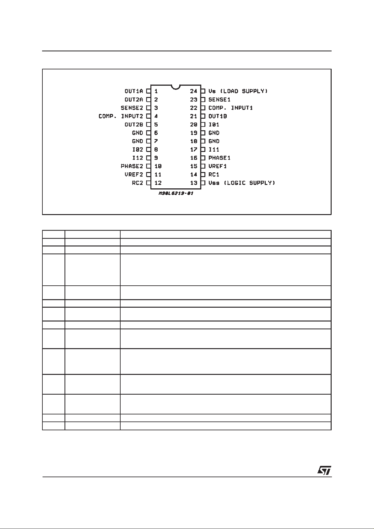
PIN CONNECTION (Top view)
PIN FUNCTIONS
N° Name Function
1;2 OUTPUT A Seepins 5;21
3;23 SENSERESISTOR Connection to Lower Emitters of OutputStage forInsertion of Current SenseResistor
4;22 COMPARATOR
INPUT
Inputconnected to the comparators. The voltage across the sense resistor is
feedback to this input throught the low pass filter RC CC. The higher power transistors
are disabled when the sense voltage exceeds the reference voltage of theselected
comparator. When this occurs the current decays for atime set by R
TCT(toff
= 1.1 R
CT). See fig. 1.
5;21 OUTPUT B Output Connection. The output stage is a ”H” bridge formed by four transistorsand
fourdiodes suitable for switching applications.
6;19 GROUND Seepins 7;18
7;18 GROUND Ground Connection. With pins 6 and 19 also conducts heat from dieto printed circuit
copper.
8;20 INPUT 0 SeeINPUT 1(pins 9;17)
9;17 INPUT 1 Thesepins and pins 8;20 (INPUT 0) are logic inputs which selectthe outputs of the
comparators to set the current level. Current also depends on the sensing resistor and
reference voltage. See Funcional Description.
10;16 PHASE This TTL-compatible logic inputs sets thedirection of currentflow through the load. A
highlevel causes current to flow from OUTPUT A (source) to OUTPUT B (sink). A
schmitt trigger on this input provides good noise immunity and a delaycircuit prevents
outputstage short circuits duringswitching.
11;15 REFERENCE
VOLTAGE
A voltage applied to thispin sets the reference voltage of the comparators, this
determining the output current (also thus depending on R
and the two inputs INPUT
s
0 and INPUT 1).
12;14 RC A parallel RC network connectedto this pinsets theOFF timeof the higher power
transistors. The pulse generator is a monostabletriggered by theoutput of the
13 V
comparators (t
- LOGIC SUPPLY Supply Voltage Input for LogicCircuitry
ss
= 1.1 RTCT).
off
24 Vs - LOAD SUPPLY Supply Voltage Input for theOutput Stages.
Note: ESD on GND, VS,VSS, OUT 1A and OUT 2Ais guaranteedup to 1.5KV (Human Body Model,1500Ω, 100pF).
T
2/8

L6219DSA
ABSOLUTE MAXIMUM RATINGS
Symbol Parameter Value Unit
V
V
V
V
sense
T
T
T
THERMAL DATA
Symbol Description Value Unit
R
thj-case
R
thj-amb
(*) With minimized copper area.
Supply Voltage 50 V
S
Output Current (peak) ±1A
I
o
Output Current (continuous) ±0.75 A
I
o
Logic Supply Voltage 7 V
SS
Logic Input VoltageRange -0.3 to +7 V
IN
Sense Output Voltage 1.5 V
Junction Temperature +150
J
Operating Temperature Range -40 to 125 °C
op
Storage Temperature Range -55 to +150 °C
stg
Thermal Resistance Junction-case Max.
Thermal Resistance Junction-ambient Max.
18
75 (*)
C
°
°C/W
C/W
°
ELECTRICALCHARACTERISTICS (Tj= -40to 125°C,VS= 46V,VSS= 4.75V to 5.25V, V
REF
less otherwisespecified)See fig. 3.
Symbol Parameter Test Condition Min. Typ. Max. Unit
OUTPUTDRIVERS (OUTAor OUTB)
I
V
CE(sat)
I
S(on)
I
S(off)
V
CEX
V
Motor Supply Range 10 46 V
S
Output Leakage Current VS = 52V V
V
= 52V V
S
Output Saturation Voltage Sink Driver, I
Sink Driver, I
Source Driver, I
Source Driver, I
Clamp Diode Forward Voltage High stage IF =750mA
F
Low stage I
= 50V
OUT
= 1V -200
OUT
= +500mA
OUT
OUT = +750mA
= -500mA
OUT
= -750mA
OUT
F =750mA
Driver Supply Current Both Bridges ON, No Load 17 mA
Driver Supply Current Both Bridges OFF 12 mA
200
0.75
1.15
1.6
1.8
1.7
1.6
CONTROLLOGIC
V
IN(H)
V
IN(L)
I
IN(H)
I
IN(L)
V
REF
I
SS(ON)
I
SS(OFF)
Input Voltage All Inputs 2.4 V
Input Voltage All Inputs 0.8 V
Input Current VIN = 2.4V <1 20 µA
Input Current VIN = 0.84V -3 -200 µA
Reference Voltage Operating 1.5 7.5 V
Total Logic Supply Current Io=I1= 0.8V, No Load 76 mA
Total Logic Supply Current Io=I1= 2.4V, No Load 15 mA
COMPARATORS
= 5V; un-
A
µ
µA
V
V
V
V
V
V
V
REF/Vsense
t
off
t
d
Current Limit Threshold (attrip
point
Io=I1= 0.8V 9.5 10 10.5
= 2.4V, I1= 0.8V 13.5 15 16.5
I
o
= 0.8V, I1= 2.4V 25.5 30 34.5
I
o
Cutoff Time Rt = 56KΩ Ct= 820pF 50 s
Turn Off Delay Fig. 1 1 sµµ
3/8
 Loading...