

ABLE TO DRIVE BOTH WINDINGS OF BIPOLAR STEPPER MOTOR
OUTPUT CURRENT UP TO 750mA EACH
WINDING
WIDEVOLTAGERANGE 10V TO 46V
HALF-STEP, FULL-STEP AND MICROSTEPP-
INGMODE
BUILT-INPROTECTIONDIODES
INTERNALPWM CURRENT CONTROL
LOW OUTPUTSATURATIONVOLTAGE
DESIGNED FOR UNSTABILIZED MOTOR
SUPPLYVOLTAGE
INTERNALTHERMAL SHUTDOWN
DESCRIPTION
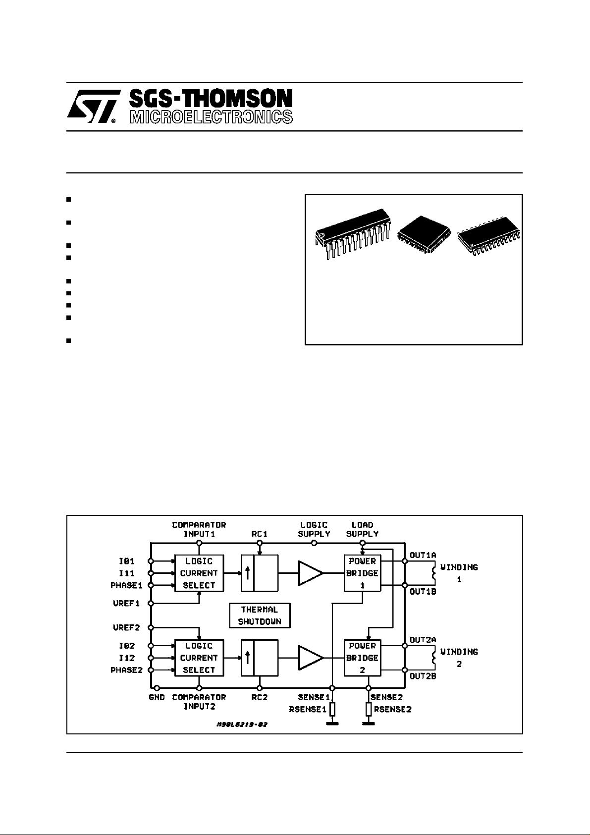
The L6219 is a bipolar monolithic integrated circuits intended to control and drive both winding of
a bipolar stepper motor or bidirectionally control
two DC motors.
The L6219 with a few external components form
a complete control and drive circuit for LS-TTL or
microprocessorcontrolledstepper motor system.
The power stage is a dual full bridge capable of
sustaining 46V and including four diodes for current recirculation.
A crossconductionprotection is providedto avoid
L6219
STEPPER MOTOR DRIVER
Powerdip 20+2+2 PLCC44 SO20+2+2
ORDERING NUMBERS:
L6219 L6219D L6219DS
simultaneous cross conduction during switching
currentdirection.
An internal pulse-width-modulation (PWM) controls the output current to 750mA with peak startup current up to 1A.
Wide range of current control from 750mA (each
bridge) is permitted by means of two logic inputs
and an external voltage reference. A phase input
to each bridge determines the load current direction.
A thermal protection circuitry disables the outputs
if the chip temperature exceeds safe operating
limits.
BLOCK DIAGRAM
December 1996
1/10
L6219
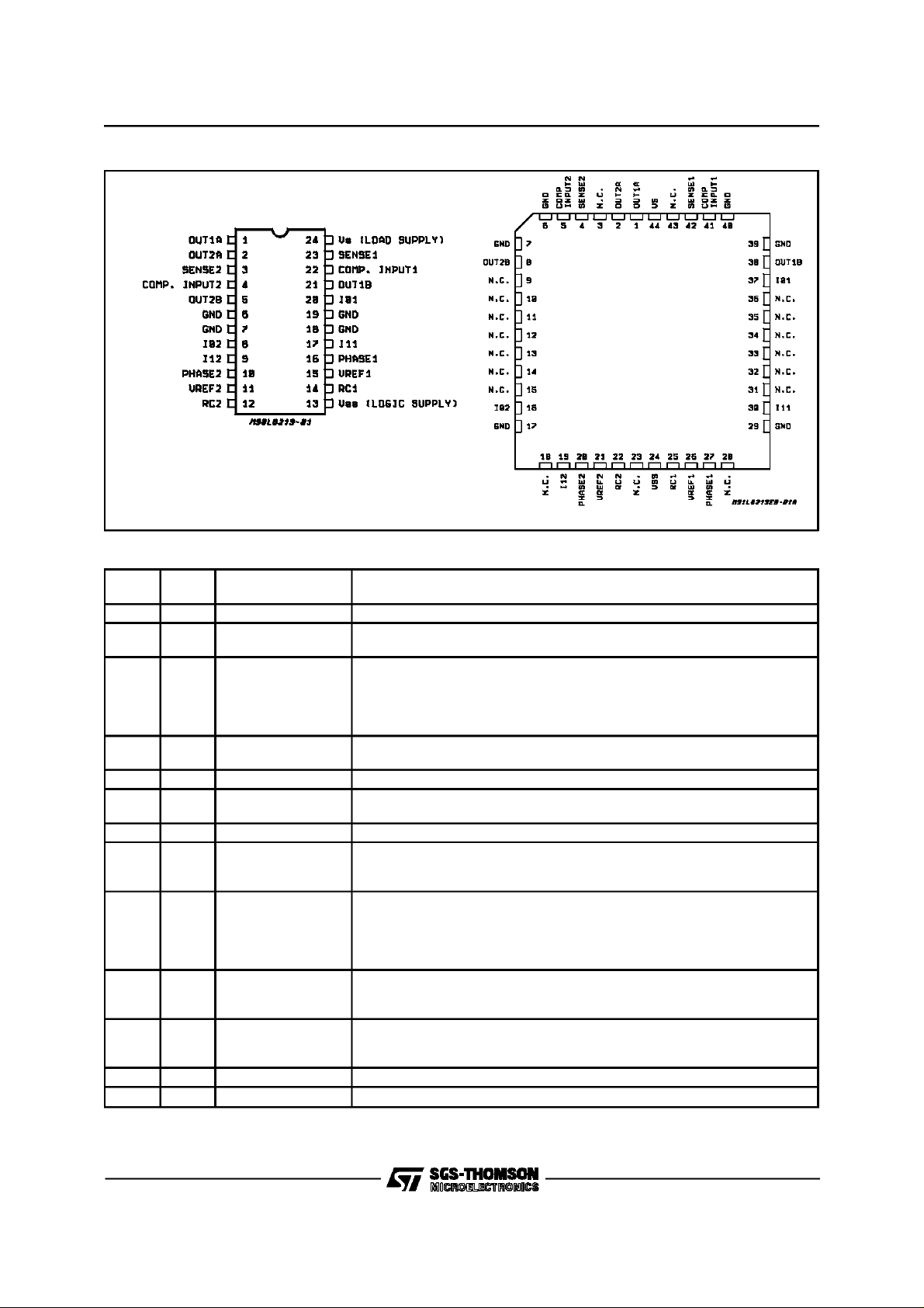
PIN CONNECTIONS (Topview)
Powerdip and SO
PIN FUNCTIONS
PLCC44
PLCC
(*)
PDIP &
SO
Name Function
1;2 1;2 OUTPUT A See pins 5;21
4;42 3;23 SENSE RESISTOR Connection to Lower Emitters of Output Stage forInsertion of Current Sense
Resistor
5;41 4;22 COMPARATOR
INPUT
Input connected to the comparators. The voltageacross the sense resistor is
feedback to this input throught the low pass filter RC CC. The higher power
transistors are disabled when the sense voltage exceeds thereference
voltage of the selected comparator.When this occurs the current decays for
a time set by R
TCT(toff
= 1.1 RTCT). See fig. 1.
8;38 5;21 OUTPUT B Output Connection. The outputstage is a ”H” bridge formedby four
transistors and four diodessuitable for switching applications.
6;7;17 6;19 GROUND See pins 7;18
29;39;407;18 GROUND Ground Connection.With pins6 and 19 also conducts heatfrom die to
printed circuit copper.
16;37 8;20 INPUT 0 See INPUT 1 (pins 9;17)
19;30 9;17 INPUT 1 These pins and pins 8;20 (INPUT 0) are logicinputs which select the outputs
of the comparators to set the current level.Current also depends on the
sensing resistor and reference voltage. See FuncionalDescription.
20;27 10;16 PHASE This TTL-compatible logic inputssets the direction of current flowthrough
the load. A high levelcauses current to flow from OUTPUT A (source)to
OUTPUT B (sink). A schmitttrigger onthis input provides good noise
immunity and adelay circuit prevents output stageshort circuits during
switching.
21;26 11;15 REFERENCE
VOLTAGE
A voltage applied to thispin sets the reference voltage of the comparators,
this determining the outputcurrent (also thus dependingon R
and the two
s
inputs INPUT 0 and INPUT 1).
22;25 12;14 RC A parallel RC network connected to this pin sets the OFF time ofthe higher
power transistors. The pulsegenerator is a monostable triggered by the
24 13 V
output of thecomparators (t
- LOGIC SUPPLY Supply Voltage Input for Logic Circuitry
ss
= 1.1 RTCT).
off
44 24 Vs - LOAD SUPPLY Supply Voltage Input forthe Output Stages.
(*)Pins: 3, 9,10,11,12,13,14,15,18,23,28,31,32,33,34,35,36,43 are Not Connected.
Note: ESD on GND, V
, OUT 1A and OUT 2Ais guaranteedup to 1.5KV (Human Body Model, 1500Ω, 100pF).
S,VSS
2/10
ABSOLUTE MAXIMUM RATINGS
Symbol Parameter Value Unit
Supply Voltage 50 V
S
Output Current (peak) ±1A
I
o
Output Current (continuous) ±0.75 A
I
o
Logic Supply Voltage 7 V
SS
Logic Input VoltageRange -0.3 to +7 V
IN
Sense Output Voltage 1.5 V
Junction Temperature +150
J
Operating Temperature Range 0 to 70 °C
op
Storage Temperature Range -55 to +150 °C
stg
V
V
V
V
sense
T
T
T
THERMAL DATA
Symbol Description PLCC PDIP SO Unit
R
thj-case
R
thj-amb
(*) With minimized copper area.
Thermal Resistance Junction-case Max.
Thermal Resistance Junction-ambient Max.1245 (*)1460 (*)1875 (*)
L6219
C
°
°C/W
C/W
°
ELECTRICALCHARACTERISTICS (Tj=25°C,VS= 46V, VSS= 4.75Vto 5.25V, V
= 5V; unlessoth-
REF
erwise specified)See fig.3.
Symbol Parameter Test Condition Min. Typ. Max. Unit
OUTPUTDRIVERS (OUTAor OUTB)
I
V
CE(sat)
I
S(on)
I
S(off)
V
CEX
I
V
Motor Supply Range 10 46 V
S
Output Leakage Current V
Output Saturation Voltage Sink Driver, I
Clamp Diode Leakage Current VR = 50V - <1 50 µA
R
Clamp Diode Forward Voltage SinkDiode
F
=Vs
OUT
V
=0
OUT
Sink Driver, I
OUT = +750mA
Source Driver, I
Source Driver, I
Source Diode I
= +500mA
OUT
OUT
OUT
=750mA
F
= -500mA
= -750mA
-
-
-
-
-
-
<1
<-1
0.3
0.7
1.1
1.3
1
1
Driver Supply Current Both Bridges ON, No Load - 8 15 mA
Driver Supply Current Both Bridges OFF - 6 10 mA
50
-50
0.6
1
1.4
1.6
1.5
1.5
CONTROLLOGIC
V
IN(H)
V
IN(L)
I
IN(H)
I
IN(L)
V
REF
I
SS(ON)
I
SS(OFF)
Input Voltage All Inputs 2.4 - - V
Input Voltage All Inputs - - 0.8 V
Input Current VIN = 2.4V - <1 20 µA
Input Current VIN = 0.84V - -3 -200
Reference Voltage Operating 1.5 - 7.5 V
Total Logic Supply Current Io=I1= 0.8V, No Load - 64 74 mA
Total Logic Supply Current Io=I1= 2.4V, No Load - 10 14 mA
COMPARATORS
µ
µA
µ
A
V
V
V
V
V
V
A
V
REF/Vsense
t
off
t
d
Current Limit Threshold (attrip
point
Cutoff Time Rt = 56KΩ Ct= 820pF - 50 s
Turn Off Delay Fig. 1 - 1 s
Io=I1= 0.8V 9.5 10 10.5 -
= 2.4V, I1= 0.8V 13.5 15 16.5 -
I
o
= 0.8V, I1= 2.4V 25.5 30 34.5 -
I
o
µ
µ
3/10
 Loading...