L6213
SOLENOID DRIVER + SWITCH MODE POWER SUPPLY
ADVANCE DATA
OPERATINGSUPPLYVOLTAGE UP TO 46V
1A POWERSUPPLY (5V)
5A SOLENOIDDRIVER
PRECISEONCHIP REFERENCE VOLTAGE
DISCONTINUOUS MODE - FREQUENCY
VARIABLE
VERYHIGH EFFICIENCY
1Ω OUTPUTDMOS (SMPS)
INTERNAL CURRENT LIMIT (SMPS SEC-
TION)
EXTERNALLY PROGRAMMABLE SOLENOID
CURRENT RISINGSLOPE
EXTERNALLY PROGRAMMABLE FIXED
HYSTERESISCONTROL
OPTIMIZED DMOS R
CHOPPING
DESCRIPTION
The L6213 is an IC containing a S.M.P.S. delivering 1A at a voltage of 5V and a section designed
to drive a solenoidwithacurrent up to5A.
The device is realized in BCD mixed technology,
which combines isolated DMOS power transistor
with CMOSand Bipolar circuitson the samechip.
The SMPSsection can deliver 1A DC with anout-
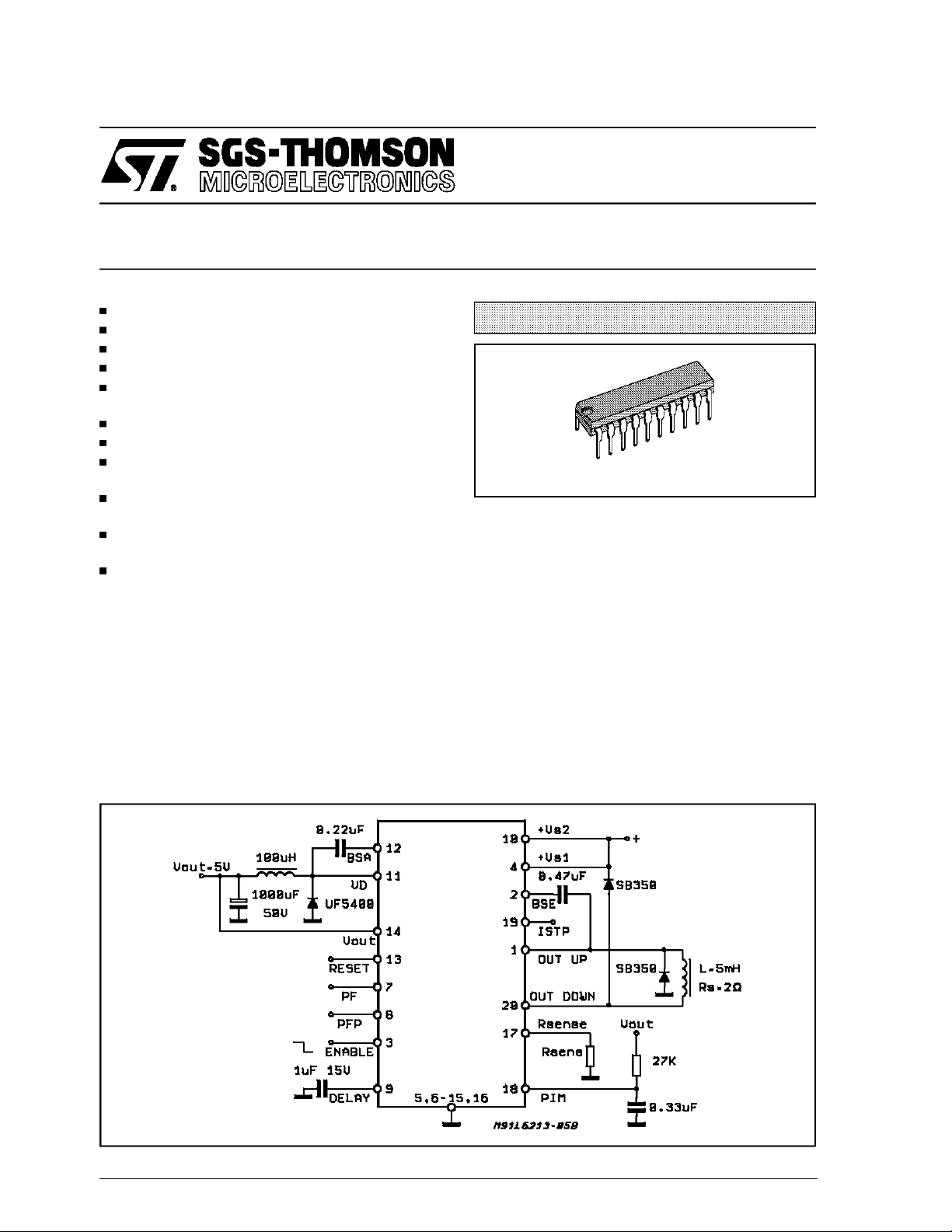
APPLICATIONCIRCUIT
DS ON
FOR HIGH SIDE
MULTIPOWERBCD TECHNOLOGY
Powerdip 16+2+2
put voltage of 5V, including current limiting, reset
and power fail for microprocessor and thermal
protection.
The solenoid driver section is designed for high
current applications like hammer driver in electronictypewriter.
Thesolenoidoutputsectioncontainsa high sideand
a low side DMOS, which R
high si de chopping.The current rising slopeisexternallyprogra mmabl ethroughanexternalcapacitor .
The level of hysteresis of the current can be
changedthroughan externalresistor.
The device is supplied in Powerdip 16+2+2, and
use the four center pins to conduct heat to the
printedcircuit.
are optimized for
DS ON
November 1991
This isadvanced information on anew product now in development or undergoing evaluation.Details are subject to change without notice.
1/9

L6213
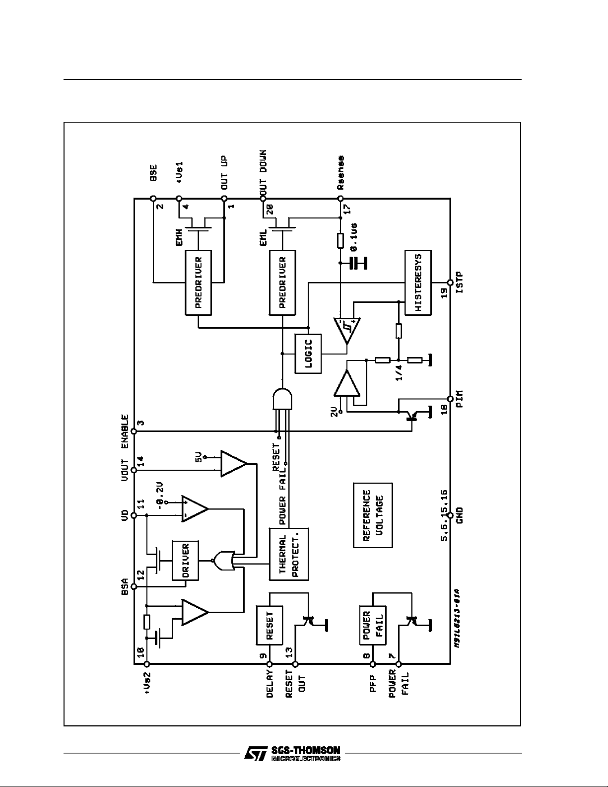
BLOCK DIAGRAM
2/9

ABSOLUTE MAXIMUMRATINGS
Symbol Parameter Value Unit
V
V
D;VOUT-UP
V
V
OUT-DOWN
V
OUT-UP
PFP Input Voltage 25 V
, Enable
V
O
PIM
Reset, PF Output Voltage 20 V
CD, ISTP Input Voltage 5.5 V
Out-Up
Out-Down
T
stg
Supply Voltage 52 V
S
Output Negative Voltage DC -1.3 V
Output Negative Voltage peak at t= 0.1µs f = 100KHz -5V V
D
Output Positive Voltage DC VS+ 1.3 V
Output Positive Voltage peak at t = 0.1µs f = 25KHz V
+5 V
S
Output Negative Voltage peak at t= 0.1µs f = 25KHz -5 V
Input Voltage 7 V
Output Current DC = 10% T
= 3.5ms 5.5 A
ON
Storage Temperature -50 to 150 °C
L6213
THERMAL DATA
Symbol Description Value Unit
R
th j-pins
R
th j-amb
Thermal Resistance Junction-pins
Thermal Resistance Junction-ambient
Max.
Max.
14
60
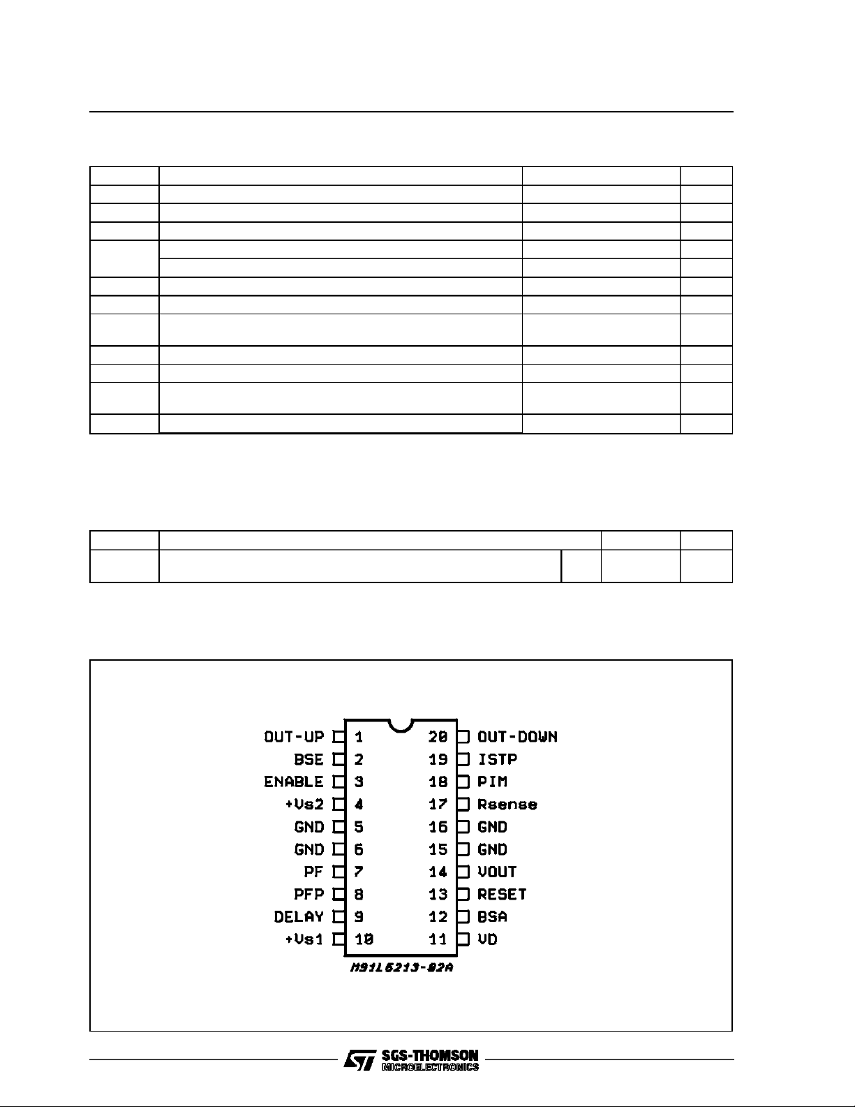
PIN CONNECTION (Top view)
°C/W
°C/W
3/9
 Loading...